A Co-Design Methodology for Energy-Efficient Multi-Mode Embedded Systems
with Consideration of Mode Execution Probabilities
Marcus T. Schmitz and Bashir M. Al-Hashimi
Dept. of Electronics and Computer Science
University of Southampton
Southampton, SO17 1BJ, United Kingdom
{m.schmitz,bmah}@ecs.soton.ac.uk
Petru Eles
Dept. of Computer and Information Science
Link¨oping University
S-58183 Link¨oping, Sweden
[email protected]Abstract
Multi-mode systems are characterised by a set of interacting operational modes to support different functionalities and stan-dards. In this paper, we present a co-design methodology for multi-mode embedded systems that produces energy-efficient im-plementations. Based on the key observation that operational modes are executed with different probabilities, i.e., the system spends uneven amounts of time in the different modes, we develop a novel co-design technique that exploits this property to signif-icantly reduce energy dissipation. We conduct several experi-ments, including a smart phone real-life example, that demon-strate the effectiveness of our approach. Reductions in power consumption of up to 64% are reported.
1
Introduction
The need for embedded systems continues to increase and power consumption has become one of the most important design ob-jectives. Over the last few year numerous methodologies for the design of low power consuming embedded systems have been proposed, among which we find approaches that leverage power management techniques, such as dynamic power management (DPM) and dynamic voltage scaling (DVS).
A key characteristic of many current and emerging embed-ded systems is their need to work across a set of different in-teracting operational modes. Such systems are called multi-mode embedded systems. Three previous approaches have addressed the problem of designing mixed hardware/software implementa-tions of multi-mode systems [7, 9, 13]. The main principle be-hind these approaches is to consider the possibility of hardware sharing, i.e., computational tasks of the same type, which can be found in different modes, utilise the same hardware compo-nent. Thereby, multiple implementations of the same task type are avoided, which, in turn, reduces the necessary hardware cost. As opposed to these approaches, the presented work addresses the design of low energy consuming multi-mode systems, hence, it differs in several aspects from the previous works. The pa-per makes the following contributions: a) We analyse the ef-fects that the consideration of mode execution probabilities has on energy-efficiency. b) A co-design methodology for the design of energy-efficient multi-mode systems is presented. We propose a co-synthesis for multi-mode systems which maps and sched-ules a system specification that captures both mode interaction and mode functionality. c) We investigate dynamic voltage scal-ing in the context of multi-mode systems and consider that not only programmable processors might be DVS enabled, but addi-tionally the hardware components.
2
Preliminaries
2.1
Functional Specification of Multi-Mode Systems
The abstract specification model we consider here is based on a combination of finite state machines and task graphs, used to cap-ture the interaction between different operational modes as well as the functionality of each individual mode. We refer to this model as operational mode state machine (OMSM). A similar model was used in [4]. However, we extend this model towards system-level design and include transition time limits as well as mode execution probabilities. The following section explains this model, using the smart phone example shown in Fig. 1a). This smart phone combines three different functionalities within one device: a GSM phone, a digital camera, and an MP3-player.
2.1.1 Top-level Finite State Machine
We consider that an application is given as a directed cyclic graph
ϒ(Ω,Θ), which represents a finite state machine. Within this top-level model, each node O∈Ωrefers to an operational mode and each edge T ∈Θspecifies a transition between two modes. If the system undergoes a change from mode Oxto mode Oy, with
x6=y, the transition time tmax
T associated with the transition edge
T = (Ox,Oy)has to be met. At any given time there is only one
active mode, i.e., the modes are mutually exclusive. Fig. 1a) ex-emplifies the operational mode state machine for a smart phone example with eight different modes. An activation scenario could look like this: When switched on, the phone initialises into Net-work Searchmode. Upon finding a network, the phone changes intoRadio Link Control (RLC) mode. In this mode it maintains the connection to the network by handling cell handovers, radio link failure responses, and adaptive RF power control. An in-coming phone call necessitates to switch intoGSM codec + RLC mode. This mode is responsible for speech encoding and decod-ing while maintaindecod-ing network connectivity. Similarly, the re-maining modes have different functions and are activated upon mode change events. Such events originate upon user requests (e.g. MP3-player activation) or are initiated by the system itself (e.g. loss of network–switch back intonetwork searchmode).
Based on the key observation that many multi-mode systems spend their operational time not evenly in each of the modes, we assume that for each operational mode O its execution probabil-ityΨOis given, i.e., we know what percentage of the operational
GSM codec + RLC
Ψ1=0.74
Ψ2=0.01
Ψ3=0.02
Ψ4=0.02
Ψ5=0.1
Ψ6=0.01
Ψ7=0.01
Ψ0=0.09
MEM
MEM ASIC
Search
Network RadioLink Control Take
Photo
Photo decode
Search + NeworkPhoto
+ RLC
+ RLC MP3 play MP3 play
+ Nework Search
Network found Network lost
Network found Network found Show
Photo Photo
Show
Incoming Call User request /
Terminate Call
audio Play audio
Play Terminate
Terminate
audio audio
Terminate TerminatePhoto
Photo
Photo Photo
taken taken
Take Photo Take Photo
decode
INIT
Interface
DVS−Contr.
CPU
Interface
DSP
BUS
SW C1: FFT
C2: HD C3: IDCT C4: Color Trans.
C5: DeQ C6: STP C7: LTP
HW
Interface C5 C6 C7
Radio Link Control decode Photo
=0.025s
HD
deQ
IDCT
Tr. color coeff. 256
256
256
256
RLC
=0.015s
θ
θ =0.025s
C2
C4
DVS−Contr.
C1
C3 Interface
FPGA
φ
a) Operational Mode State Machine b) Task Graph of a Single Mode c) Possible Target Architecture
[image:2.612.60.526.35.197.2]Network found Network lost
Figure 1. Architectural and Specification Model
on statistical information collected from several different users. Taking this information into account will prove to be important when designing systems with a prolonged battery life-time.
2.1.2 Functional Specification of Individual Modes
The functional specification of each mode O∈Ωin the top-level finite state machine is expressed by a task graph GOS(
T
,C
); see Fig. 1b). Here, each nodeτ∈T
represents a task, an atomic unit of functionality that needs to be executed without preemption. We consider a coarse level of granularity where tasks refer to func-tions such as Huffman decoders, de-quantizers, FFTs, IDCTs, etc. Therefore, each task is further associated with a task typeη∈ΓO.A distinctive feature of multi-mode systems is that task type sets
ΓO of different modes O∈Ωcan intersect, i.e., tasks of
identi-cal type can share the same hardware resource. Of course, re-source sharing is also possible for multiple tasks of identical type which are found in a single mode, however, due to task commu-nalities among different modes the chances to share resources are increased. Edgesγ∈
C
in the task graph refer to precedence con-straints and data dependencies between the computational tasks, i.e., if two tasks,τiandτj, are connected by an edge, then taskτimust have finished and transfered its data to taskτj, beforeτjcan
be executed. A feasible implementation needs to obey all timing constraints and precedence relations.
2.2
Architectural Model and System Implementation
Our system-level synthesis approach targets distributed architec-tures that possibly consist of several heterogeneous processing el-ements (PEs), such as general purpose processors (GPPs), ASIPs, ASICs, and FPGAs. These components are connected through an infrastructure of communication links (CLs). A directed graph GA(
P
,L
)captures such an architecture, where nodesπ∈P
andedgesλ∈
L
denote PEs and CLs, respectively; Fig. 1c) shows an example architecture.Since each task might have multiple implementation alterna-tives, it can be potentially mapped onto several different PEs that are capable to perform this type of task. However, if a task is mapped to a hardware component, i.e., ASIC or FPGA, a core for this task type needs to be allocated, involving the usage of area. Tasks assigned to GPPs or ASIPs (software tasks) need to be sequentialised whilst the tasks mapped onto FPGAs and ASICs (hardware tasks) can be performed in parallel if the nec-essary resources (cores) are not already engaged. However, con-tention between two or more tasks assigned to the same hardware core necessitates a sequential execution order, similar to software tasks. Cores implemented on FPGAs can be dynamically recon-figured during a mode change, involving a time overhead which
needs to respect the imposed maximal mode transition times. Further, PEs might feature dynamic voltage scaling to enable a tradeoff between power consumption and performance which can be exploited during run-time. For such PEs a voltage schedule needs to be derived, additionally to a timing schedule [10].
To implement a multi-mode application captured as OMSM, the tasks and communications of all operational modes need to be mapped onto the architecture, and a valid schedule for these activ-itiesε∈(
A
=T
∪C
)needs to be constructed. Further, for tasks mapped to DVS enabled components an energy reducing voltage schedule has to be determined. Hence, an implementation candi-date can be expressed through four functions which need to be de-rived for each operational mode O∈Ω: MτO:T
→π, MOγ :C
→λ, SOε :
A
→R+0, and VτO:T
DV S→Vπ
, where MτOand MγOdenotetask and communication mapping, respectively. Activity start times are specified by the scheduling function SOε, while VτO de-fines the voltage schedule for all tasksτ∈
T
DV Smapped toDVS-PEs, where
Vπ
is the set of the possible discrete supply voltages of PEπ. Clearly, the mappings as well as the corresponding sched-ules are defined for every mode separately, i.e., during the change from mode Ox to mode Oy, the execution of activities found inmode Oxare finished, and the activities of mode Oyare activated.
2.3
Motivational Example
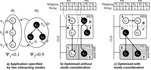
The influence of mapping in the context of multi-mode systems with different mode execution probabilities is demonstrated in the following example. For simplicity we neglect timing and commu-nication issues here. Consider the application shown in Fig. 2 a) which consists of two operational modes, O1and O2, each
spec-ified by a task graph with three tasks. The system spends 10% of its time in mode O1and the remaining 90% in mode O2, i.e.,
the execution probabilities are given byΨ1=0.1 andΨ2=0.9.
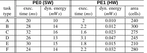
The specification needs to be mapped onto an architecture built of a general purpose processor (PE0) and an ASIC (PE1), linked by a bus (CL0). Depending on the task mapping to either of the components, the execution properties of each task are given in the following table. It can be observed that all tasks are of different
PE0 (SW) PE1 (HW)
task exec. dyn. energy exec. dyn. energy area type time (ms) (mW s) time (ms) (mW s) (cells)
A 20 10 2 0.010 240
B 28 14 2.2 0.012 300
C 32 16 1.6 0.023 275
D 26 13 3.1 0.047 245
E 30 15 1.8 0.015 210
F 24 14 2.2 0.032 280
[image:2.612.329.580.625.716.2]τ1
τ2
τ3
String Mapping
Ψ =0.11 Ψ =0.92
η1=A
η2=B
η3=C
η4=D
η6=F
O1 O2
τ1 τ2 τ3 τ4 τ5 τ6 τ1 τ2 τ3 τ4 τ5 τ6
O2 O1 O2
O1
τ3 τ2 τ1
PE0
PE1
CL0
mode consideration
PE1 PE0
CL0
τ1
τ4 τ2
τ3
τ6
τ5
mode consideration
area=600 area=600
a) Application specified by two interacting modes
b) Optimised without c) Optimised with 0 0 1 0 1 0 0 0 0 1 1 1
A
B
C
D
E F
A
C B
D
E
F
String Mapping
η5=E
τ4
6
τ5 τ
τ4
τ6
[image:3.612.326.576.33.134.2]τ5
Figure 2. Example 1: Mode Execution Probabilities
be allocated explicitly for that task. Hence, in this particular ex-ample, we do not consider hardware sharing. Each allocated core uses area on the hardware component which offers 600 cells, i.e., at most 2 cores can be allocated at the same time without violating the area constraint (see above table, column 6). Note, although the two modes execute mutually exclusive, the task types imple-mented in hardware (cores) cannot be changed during run-time, since their implementation is static (non-reconfigurable ASIC).
Consider the mapping shown in Fig. 2b). This represents the optimal solution in terms of energy dissipation when ne-glecting the execution probabilities, since the highest energy dissipating task (τ3 andτ5) are executed using a more
energy-efficient hardware implementation. Nevertheless, taking the real behaviour into account, mode O1 is active for 10% of the
op-erational time, i.e., its energy dissipation can then be calculated as 0.1·(10mW s+14mW s+23µW s) =2.4023mW s. Similarly, mode O2is active 90% of the time, hence, its energy is given by
0.9·(13mW s+15µW s+14mW s) =24.3135mW s. Based on both modes, the total energy dissipation results in 26.7158mW s.
Fig. 2c) shows an alternative mapping which represents the optimal assignment of tasks when mode execution probabil-ities are considered. In this configuration tasks τ5 and τ6
use a hardware implementation. According to this solution, the energy dissipation of mode 1 and mode 2 are given by 0.1·(10mW s+14mW s+16mW s) =4mW s and 0.9·(13mW s+
15µW s+32µW s) =11.7423mW s, respectively. The total energy for this mapping is 15.7423mW s, hence, it is 41% lower com-pared to the first mapping shown in Fig. 2b), which is not op-timised for an uneven task execution probability. Furthermore, the second task mapping, shown in Fig. 2c), allows to switch-off PE1 and CL0 during mode O1, since all tasks of this mode are
as-signed to PE0. This results in a significant reduction of the static power, further increasing the energy savings.
An important characteristic of multi-mode systems is that tasks of the same type might be found in different operational modes, i.e., resources can be shared among the different modes. To increase the possibility of component shut-down, it might be necessary to implement the same task type multiple times, how-ever, on different components. The following example, shown in Fig. 3, clarifies this aspect. Here tasksτ1andτ4are of type A,
allowing resource sharing. In the first mapping, given in Fig. 3 b), both tasks utilise the same HW core. However, additionally im-plementing task τ4 as software, as shown in Fig. 3c), allows
to shut-down PE1 and CL0 during the execution of mode O2.
Hence, multiple implementations of task types can help to reduce power dissipation.
These two examples show that it is essential to guide the syn-thesis process by an energy model that takes into account the ex-ecution probability and allows multiple task implementations.
η5=D η6=E
η1=A
η2=B
η3=C
τ2
τ3
O1 O2
τ3 τ2 τ1
τ1 τ2
τ3
η4=A
PE1 PE0
CL0
A D E
B
τ1
A
a) Application with resource sharing possibility
b) Resource sharing, but no shut−down possible
c) No resource sharing, but component shut−down
τ4
τ5 τ6 PE1
PE0
CL0
A D E
B
τ5 τ6
τ4
τ5 τ6
τ4
[image:3.612.51.311.37.157.2]C C
Figure 3. Example 2: Multiple Task Implementations
3
Problem Formulation
Our goal is an energy-efficient and feasible implementation of ap-plicationϒ, modelled as an OMSM. This involves the derivation of the mapping and schedule functions (MτO, MγO, SOε, and VτO), see Section 2.2, under the consideration of static and dynamic power dissipations as well as mode execution probabilities. The average power consumption ¯p of an implementation alternative is given by:
¯ p=
∑
O∈Ω
(p¯dynO +p¯statO )·ΨO (1)
where ¯pdynO , ¯pstatO , andΨOrefer to the dynamic power
consump-tion, the static power consumpconsump-tion, and execution probability of mode O, respectively. The power consumptions are given as,
¯
pdynO =
∑
ε∈AO
E(ε)
! · 1
hpO
and p¯statO =
∑
ξ∈KO
¯ Pstat(ξ)
where
A
Oand hpOare all activities and the hyper-period of modeO, respectively. ¯Pstat(ξ)refers to the static power consumption of a component ξ, found in the set of all active components
K
O⊆P
∪L
of mode O. With respect to the type of activities,the dynamic energy consumption E(ε)is calculated as,
E(ε) =
Pmax(ε)·tmin(ε)· V2
dd(ε)
V2
max(ε) ifε∈
T
DVSPmax(ε)·tmin(ε) ifε∈
T
\T
DVSPC(ε)·tC(ε) ifε∈
C
where Pmax is the dynamic power dissipation and tminthe
execu-tion time of tasks when executed at nominal supply voltage Vmax.
Tasksτ∈
T
DVSmapped to DVS-PEs can execute at a scaledsup-ply voltage Vdd, resulting in a reduced power consumption.
Fur-ther, communications consume power PCover a time tC.
The synthesis goal is to find a task mapping MOτ, a commu-nication mapping MOγ, a time schedule SOε, and a voltage sched-ule VO
τ for each operational mode O, such that the total average
power ¯p, given in Equation (1), is minimised. A feasible imple-mentation candidate needs to fulfil the following requirements: a) The mapping of tasks MOτ does not violate area constraints, i.e., (∑η∈Γπaη)≤amaxπ , ∀π∈
P
; where Γπ is the set of all task types implemented on PE π, and aη and amaxπ refer to the area used by task typeηand the available area on PEπ, respec-tively. b) The timing schedule SOε and the voltage schedule VτO,
based on task and communication mapping, do not exceed any task deadlines θτ or task graph repetition periods φ, therefore, tS(τ) +texe(τ)≤min(θτ,φ), ∀τ∈
T
; where tS(τ)and texereferto task start time and task execution time (potentially based on voltage scaling), respectively. c) The system reconfiguration time tT between mode changes does not exceed the imposed maximal
mode transition times tmax
T . Hence, tT ≤tTmax, ∀T∈Θ, needs to
be respected for all mode transitions.
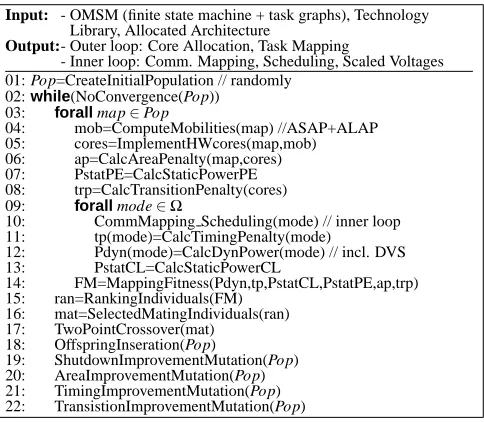
Input: - OMSM (finite state machine + task graphs), Technology
Library, Allocated Architecture
Output:- Outer loop: Core Allocation, Task Mapping
- Inner loop: Comm. Mapping, Scheduling, Scaled Voltages 01: Pop=CreateInitialPopulation // randomly
02:while(NoConvergence(Pop)) 03: forallmap∈Pop
04: mob=ComputeMobilities(map) //ASAP+ALAP 05: cores=ImplementHWcores(map,mob) 06: ap=CalcAreaPenalty(map,cores) 07: PstatPE=CalcStaticPowerPE 08: trp=CalcTransitionPenalty(cores) 09: forallmode∈Ω
10: CommMapping Scheduling(mode) // inner loop 11: tp(mode)=CalcTimingPenalty(mode)
12: Pdyn(mode)=CalcDynPower(mode) // incl. DVS 13: PstatCL=CalcStaticPowerCL
14: FM=MappingFitness(Pdyn,tp,PstatCL,PstatPE,ap,trp) 15: ran=RankingIndividuals(FM)
16: mat=SelectedMatingIndividuals(ran) 17: TwoPointCrossover(mat)
18: OffspringInseration(Pop)
[image:4.612.59.301.33.244.2]19: ShutdownImprovementMutation(Pop) 20: AreaImprovementMutation(Pop) 21: TimingImprovementMutation(Pop) 22: TransistionImprovementMutation(Pop)
Figure 4. Pseudo Code: Multi-Mode Task Mapping GA
optimises task mapping and core allocation while the inner loop is responsible for the optimisation of communication mapping and scheduling. Due to the space limitations we focus here on the mapping and core allocation, which are explained next, and refer the interested reader to [12] were communication mapping and scheduling are outlined.
4.1
Task Mapping and Core Allocation Approach
The presented task mapping approach, which determines Mτfor all modes of applicationϒ, is based on a genetic algorithm (GA). More exactly, we have extended a GA mapping technique for sin-gle mode systems [11] to suit the particular problems of multi-mode systems. These problems include resource sharing, compo-nent shut-down, and mode transition issues.
In general, GAs optimise a population of individuals over sev-eral generations by imitating and applying the principles of natu-ral selection. I.e., the GA iteratively evolves new populations by mating (crossover) the fittest individuals (highest quality) of the current population pool until a certain convergency criterion is met. In addition to mating, mutation, that is, the random change of genes in the genome (string), provides the opportunity to push the optimisation into unexplored search space regions. An excel-lent introduction to GA can be found in [3]. In our case, each mapping candidate is encoded into a multi-mode mapping string as shown in Fig. 2b) and Fig. 2c). A detailed description of the proposed mapping GA is outlined in Fig. 4.
Starting from an initial random population (line 1), the opti-misation runs until the convergency criterion is met (line 2). The criterion we use is based on the diversity in the current popula-tion and the number of elapsed iterapopula-tions without any improved individual. To judge the quality of mapping candidates, i.e., the fitness which guides the genetic algorithm, it is necessary to es-timate important design objectives, including static and dynamic power dissipation, area usage, and timing behaviour (lines 03– 13). The following explains each of the estimations. The hard-ware area depends on the allocated cores. Of course, for each task type mapped to hardware at least one core of this type needs to be allocated. However, if too many cores are placed onto an ASIC or FPGA, the available area is exceeded and an area penalty is introduced (line 6). On the other hand, if multiple tasks of the same type are mapped to the same hardware component and the hardware area is not violated, it is possible to implement cores
multiple times. In our approach, we allocated additional cores (line 5) for parallel tasks with low mobility (line 4), therefore, the chance to exploit application parallelism is increased. Clearly, from an energy point of view, this is also preferable, especially in the presence of DVS, where a decreased execution time can be exploited. At this point it is possible to compute the static power consumption of the implementation (line 7), taking into account component shut-down. Components can be shut-down during the execution of a certain mode, whenever no tasks belonging to that mode are mapped onto these components. Another aspect is the reconfigurability of FPGAs which allows to exchange the cores to suit the active mode. However, this reconfiguration during a mode change takes time, hence, we introduce a transition penalty if the maximal transition times are exceeded (line 8). Having de-termined the cores to be implemented (line 5), it is now possible to schedule each mode of the application and to derive a feasible communication mapping (line 10). Since the modes are mutually exclusive, it is possible to employ a communication mapping and scheduling optimisation for a single mode system. We utilise the technique outlined in [12]. If timing constraints are violated by the found schedule, a timing penalty is introduced (line 11). Fur-ther, based on the communication mapping and scheduling, the dynamic power consumption of the application can be computed, taking into account DVS (line 12). Similarly to the shut-down of PEs, it is also possible to switch-off a CL when no communica-tions are mapped to that link (line 13). Based upon all estimated power consumptions and penalties, a fitness is calculated (line 14) as, FM =p¯·t p·(1+wA·∑π∈Pv(a
U
π −amaxπ )/(amaxπ ·0.01))· (wR·∏T∈ΘvtT/tTmax), where the energy consumption ¯p is given
by Equation (1) and t p introduces a timing penalty. Further, an area penalty is applied for all PEs with area violation
P
vbyrelat-ing used area aUπ and area constraint amaxπ . Similarly, a transition time penalty is applied for all transitions that exceed their maxi-mal transition time limitΘv, i.e., transition time tT exceeds
maxi-mal allowed transition time tTmax. Both area and transition penalty are weighted (wAand wR) which allows to adjust the
aggressive-ness of the penalty. Having assigned a fitaggressive-ness to all individuals of the population, they are ranked using linear scaling (line 15). A tournament selection scheme picks individuals (line16) for mat-ing (line 17). The produced offsprmat-ings are inserted into the pop-ulation (line 18). In order to push the GA away from infeasible and low quality design space regions, we apply four new genetic mutation operators (lines 19–22), introduced next.
Shut-down Improvement: To increase the chances of
compo-nent shut-down, which leads to a reduction of static power con-sumption, we employ a simple yet effective strategy during the optimisation. Out of the current population randomly picked in-dividuals (probability 2% was found to lead to good results) are modified as follows. A single mode Oxand a non-essential PE πaare selected. Non-essential PEs are considered to be PEs that
implement task types that have alternative implementations on other PEs, hence, they are not fundamental for a feasible solu-tion. Our goal is to switch-off PEπa during the execution of
mode Ox. Therefore, all tasks of mode Oxwhich are mapped to πaare randomly re-mapped to the remaining PEs (
P
\πa), hence,PEπacan be shut-down during mode Ox.
Area Improvement: To avoid convergency towards area
τ1 τ2 τ0
τ3 τ4
τb
τa τc
τ1 τ2
τ0 τ3 τ4
core 0
core 1
Transformation
τb
τa τc
core A
tS1 tE2 tSb tEb
core 0
Hardware Component
core 1 core A
Transformed HW Component
Figure 5. DVS Transformation for HW Cores
Timing Improvement: In contrast to the area improvement
strat-egy, if a certain amount of timing infeasible solutions have been produced, software tasks are randomly mapped to faster hardware implementations. Thereby, the chance to find timing feasible im-plementations is increased.
Transition Improvement: As mentioned above, cores
imple-mented on FPGAs can be dynamically reconfigured, involving a time overhead. If this overhead exceeds the imposed transition time limits, the mapping is infeasible. Hence, after generating for a certain number of generations solely solutions that violate the transition times, tasks are randomly re-mapped away from the FPGAs that cause the violations.
Although some of the produced genomes might be infeasible in terms of area and timing behaviour, all these strategies have been found to improve the search process significantly by intro-ducing individuals that evolve into high quality solutions.
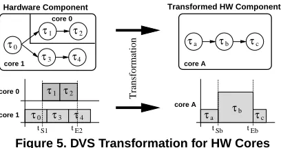
4.2
Dynamic Voltage Scaling in Multi-Mode Systems
Dynamic voltage scaling is a powerful technique to reduce en-ergy consumption by exploiting temporal performance require-ments through dynamically adapting processing speed and sup-ply voltage of PEs. The applicability of DVS to embedded dis-tributed systems was demonstrated in [5, 8, 10]. However, these papers concentrated on dynamically changing the performance of software PEs only, while parallel execution of tasks on hard-ware resources has been neglected. Nevertheless, in the context of energy-efficient multi-mode systems, where performance re-quirements of each operational mode can vary significantly, DVS needs to be considered carefully. For instance, consider an in-verse DCT algorithm, used by the MP3 decoder and the JPEG image decoder, implemented in fast hardware. Clearly, the JPEG decoder should restore images as quickly as possible (maximal clock frequency), while the MP3 decoder works at a fixed sam-pling rate of 25ms (reduced clock). Using DVS it is possible to adapt the HW core speed to suit both needs and reduce the energy dissipation to a minimum.
In this work, we consider that hardware components might em-ploy DVS. However, due to the area and power overhead involved in additional DVS hardware (DC/DC converter), we take into ac-count that all cores allocated to the same hardware component are fed by a single voltage supply, i.e., dynamically scaling the sup-ply voltage simultaneously affects the performance of all cores on that component.
To cope with this, we transform the potentially parallel exe-cuting tasks on a single scalable hardware resource into an equiv-alent set of sequentially executing tasks, taking into account the dynamic power dissipation on each core. Note that this is done to calculate the scaled supply voltages only, i.e., this virtual trans-formation does not affect the real implementation. Fig. 5 shows the transformation of 5 hardware tasks, executing on two cores, to 3 sequential tasks on a single core. This sequential execution is equivalent to the behaviour of software tasks, hence, a voltage
Example without probab. with probab. (proposed) (No. of Power ¯p CPU time Power ¯p CPU time Reduc.
modes) (mW ) (s) (mW ) (s) (%)
mul1 (4) 8.131 20.7 7.529 24.7 7.29
mul2 (4) 3.404 15.5 2.771 18.2 18.61
mul3 (5) 10.923 23.4 10.430 23.0 4.17
mul4 (5) 7.975 21.0 6.726 25.2 15.50
mul5 (3) 5.186 18.4 4.668 22.1 10.01
mul6 (4) 1.677 20.6 1.301 19.9 22.46
mul7 (4) 3.306 11.6 1.250 21.4 62.18
mul8 (4) 1.565 32.1 1.329 28.0 15.06
mul9 (4) 3.081 6.0 1.901 5.8 38.28
mul10 (5) 1.105 28.3 0.941 32.1 14.83
mul11 (3) 2.199 9.3 1.304 16.6 40.70
[image:5.612.76.280.35.143.2]mul12 (4) 7.006 25.4 5.975 34.2 14.69
Table 1. Considering Execution Probabilities (w/o DVS)
scaling technique for software processors can be applied.
5
Experimental Results
Our co-synthesis approach for energy-efficient multi-mode sys-tems has been implemented on a Pentium III/1.2GHz Linux PC. In order to evaluate its capability to produce high quality solutions in terms of energy consumption, timing behaviour, and hardware area requirements, a set of experiments has been carried out on 12 automatically generated examples (mul1–mul12) and one real-life benchmark (smart phone). All reported results were obtained by running the optimisation processes 40 times and av-eraging the outcomes.
Each of the 12 generated examples is specified by 3 to 5 oper-ational modes, each consisting of 8 to 32 tasks. The used target architectures contain 2 to 4 heterogeneous PEs, some of which are DVS enabled. These PEs are connected by 1 to 3 CLs.
To illustrate the importance of taking mode execution prob-abilities into account during the synthesis process, we compare an execution probability neglecting approach with our synthesis technique. Tab. 1 shows this comparison for the 12 generated benchmarks. Columns 2 and 3 give the dissipated average power and optimisation time for the execution probability neglecting ap-proach while Columns 4 and 5 show the same for the proposed approach. Take, for instance, examplemul6. Ignoring the ex-ecution probabilities during the optimisation an average power of 1.677mW is achieved. However, the optimisation under the consideration of the real-world characteristic that modes execute with uneven probabilities the average power can be reduced by an appropriate task mapping and core allocation to 1.301mW . This is a significant reduction of 22.46%. Furthermore, it can be ob-served that the proposed technique was able to reduce the energy dissipation of all examples with up to 62.18%. Note that these reductions are achieved without a modification of the underlying hardware architectures, i.e., the system costs are not increased. It is also important to note that the achieved energy reductions are solely introduced by taking the mode execution probabilities into account during the synthesis process, i.e., both compared ap-proaches allow the same resource sharing and rely on the same scheduling technique. Comparing the optimisation times for both approaches it can be observed that the proposed technique shows a slight increased CPU time for most examples, which is mainly due to the design space structure.
Example without probab. with probab. (proposed) (No. of Power ¯p CPU time Power ¯p CPU time Reduc.
modes) (mW ) (s) (mW ) (s) (%)
mul1 (4) 4.271 526.6 3.964 768.6 10.92
mul2 (4) 1.568 860.4 1.273 687.4 18.82
mul3 (5) 4.012 1053.5 3.344 1192.2 16.66 mul4 (5) 2.914 1135.2 2.320 1125.4 20.39
mul5 (3) 1.394 967.7 1.315 932.1 5.68
mul6 (4) 0.689 472.9 0.465 593.7 32.53
mul7 (4) 1.331 540.3 0.479 820.7 64.02
mul8 (4) 0.564 1262.1 0.436 1412.0 22.64
mul9 (4) 0.942 161.2 0.648 177.1 34.66
[image:6.612.329.576.36.88.2]mul10 (5) 0.480 1456.3 0.394 1361.9 17.88 mul11 (3) 0.396 318.1 0.255 403.2 35.53 mul12 (4) 2.857 1384.7 2.460 1450.7 13.91
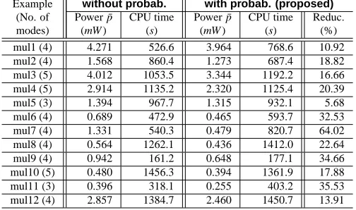
Table 2. Experimental Results with DVS
enables the consideration of DVS not only for software proces-sor but also for parallel executing cores on hardware PEs (see Section 4.2.) As in the first experiments, we compare two ap-proaches, one neglecting the mode execution probabilities during optimisation, while the second takes them into account through-out the synthesis. Similar to Tab.1, Column 2 and 3 of Tab. 2 show the results without consideration of execution probabilities, whilst Column 4 and 5 present the results achieved by the pro-posed approach. Lets consider againmul6. Although the exe-cution probabilities are neglected in Column 2, we can observe a reduced average power dissipation (0.689mW ) when compared to the results given in Tab. 1. This clearly demonstrates the high energy reduction capabilities of DVS. Nevertheless, it is possible to further minimise the average power to 0.465mW by consider-ing the execution probabilities together with DVS. This is an im-provement of 32.53%. For all other benchmarks, savings of up to 64.02% were achieved. Due to the computation of scaled supply voltages and the influence of scheduling on the energy dissipa-tion, the optimisation times are higher when DVS is considered.
To further validate the proposed co-synthesis technique in terms of real-world applicability, we applied our approach to a smart phone real-life example. This benchmark is based on three publicly available applications: a GSM codec [1], a JPEG de-coder [2], and an MP3 dede-coder [6], Based on these applications, the smart phone offers three different services to the user, namely, a GSM cellular phone, an MP3-player, and a digital camera. Of course, the used applications do not specify the whole smart phone device, however, a major digital part of it. The OMSM for this example is shown in Fig. 1a). For each of the eight op-erational modes we have extracted the corresponding task graphs from the above given references. These have been software pro-filed to extract the necessary execution characteristics of each task. On the other hand, the hardware estimations are not based on direct measurements but have been based on realistic assump-tions, such that hardware tasks typically executed 5 to 100 times faster than their software counterparts. Depending on the oper-ational mode, the number of tasks and communications varies between 5–88 nodes and 0–137 edges, respectively. The given system architecture consists of one DVS enabled GPP and two ASICs which are connected through a single bus.
Table 3 shows the results of our experiments. Similar to the previous experiments, we compare an execution probabilities ne-glecting approach with the proposed technique. The first row in Table 3 shows this comparison for a fixed voltage system. Syn-thesising the system without consideration of execution proba-bilities, results in an average power of 2.602mW . Nevertheless,
without probab. with probab. (proposed) Smart Power ¯p CPU time Power ¯p CPU time Reduc.
phone (mW ) (s) (mW ) (s) (%)
w/o DVS 2.602 80.1 1.801 96.9 30.76
with DVS 1.217 3754.5 0.859 4344.8 29.41
Table 3. Results of Smart Phone Experiments
taking into account the mode usage profile, this can be reduced by 30.76% to 1.801mW . We have also applied DVS to this bench-mark, considering that the GPP of the given architecture supports DVS functionality (see second row in Table 3). We can observe that the power dissipation drops to 1.217mW , even when neglect-ing mode execution probabilities. However, the combination of applying DVS and taking execution probabilities into account, results in the lowest power dissipation of 0.859mW , a 29.41% reduction. Overall, decreasing the average power from 2.602mW to 0.859mW . This is a significant reduction of nearly 67%.
6
Conclusions
We have proposed a novel co-design methodology for energy-efficient multi-mode embedded systems. Unlike previous ap-proaches, the presented co-design technique optimises mapping and scheduling not only towards hardware cost and timing be-haviour, but additionally reduces power consumption. The key contribution was the development of an effective mapping strat-egy that considers uneven mode execution probabilities as well as several other important power reduction aspects, such as multiple task implementations. For this purpose, we have introduced a GA based mapping approach along with four improvement strategies that guide the mapping optimisation towards high quality solu-tions in terms of power consumption, timing feasibility, and area usage. We have validated our approach using several experiments including a smart phone real-life example. These experiments have demonstrated that it is important to take mode execution probabilities into account.
References
[1] GSM 06.10, Technical University of Berlin. Source code available at http://kbs.cs.tu-berlin.de/∼jutta/toast.html.
[2] Independent JPEG Group: jpeg-6b. Source code available at ftp://ftp.uu.net/graphics/jpeg/jpegsrc.v6b.tar.gz.
[3] D. E. Goldberg. Genetic Algorithms in Search, Optimization & Machine Learning. Addison-Wesley, 1989.
[4] T. Gr¨otker, R. Schoenen, and H. Meyr. PCC: A Modeling Technique for Mixed Control/Data Flow Systems. In Proc. ED&TC 97, March 1997. [5] F. Gruian and K. Kuchcinski. LEneS: Task Scheduling for Low-Energy
Systems Using Variable Supply Voltage Processors. In Proc. ASP-DAC’01, pages 449–455, Jan 2001.
[6] J. Hagman. mpeg3play-0.9.6. Source code available at http://home.swipnet.se/∼w-10694/tars/mpeg3play-0.9.6-x86.tar.gz. [7] A. Kalavade and P. A. Subrahmanyam. Hardware/software Partitioning
for Multifunction Systems. IEEE Trans. CAD, 17(9):819–837, September 1998.
[8] J. Luo and N. K. Jha. Battery-Aware Static Scheduling for Distributed Real-Time Embedded Systems. In Proc. DAC01, 2001.
[9] H. Oh and S. Ha. Hardware-Software Cosynthesis of Mode Multi-Task Embedded Systems with Real-Time Constraints. In CODES’02, pages 133–138, May 2002.
[10] M. T. Schmitz and B. M. Al-Hashimi. Considering Power Variations of DVS Processing Elements for Energy Minimisation in Distributed Sys-tems. In Proc. ISSS’01, pages 250–255, October 2001.
[11] M. T. Schmitz, B. M. Al-Hashimi, and P. Eles. Energy-Efficient Mapping and Scheduling for DVS Enabled Distributed Embedded Systems. In Proc. DATE02, pages 514–521, March 2002.
[12] M. T. Schmitz, B. M. Al-Hashimi, and P. Eles. Synthezing Energy-Efficient Embedded Systems with LOPOCOS. Design Automation for Embedded Systems, 6(4):401–424, July 2002.
[image:6.612.53.305.37.186.2]