Motorola reserves the right to make changes without further notice to any products herein. Motorola makes no warranty, representation or guarantee regarding the suitability of its products for any particular purpose, nor does Motorola assume any liability arising out of the application or use of any product or circuit, and specifically disclaims any and all liability, including without limitation consequential or incidental damages. “Typical” parameters which may be provided in Motorola data sheets and/or specifications can and do vary in different applications and actual performance may vary over time. All operating parameters, including “Typicals” must be validated for each customer application by customer’s technical experts. Motorola does not convey any license under its patent rights nor the rights of others. Motorola products are not designed, intended, or authorized for use as components in systems intended for surgical implant into the body, or other applications intended to support or sustain life, or for any other application in which the failure of the
SPI
Block Guide
V03.06
Original Release Date: 21 JAN 2000 Revised: 04 FEB 2003
Revision History
Version Number Revision Date EffectiveDate Author Description of Changes
0.1 21 Jan 2000
This spec is based on the Barracuda, with modifications to change the module from 16 bit to 8 bit.
0.2 1 Mar
2000 Template of this document changed as per Version 2.0 SRS.
0.3 14 Jun 2000
- Signal names are changed as per the SRS2.0 - SPE bit remains set in the Mode Fault error case - Slave SPI does not support div2 and div4 cases
0.4 31 Aug 2000
- Electrical spec added
- SPIF flag is cleared by a read access to the status register followed by read access to the data register.
0.5 13 Mar 2001
13 Mar 2001
- Incorporated feedback regarding format of the document.
0.6 13 Mar 2001
19 Mar 2001
- Incorporated changes as a result of internal discussions and clarification of SRS2
0.7 6 July 2001
6 July 2001
- Line is added with respect to SPTEF bit to make spec more clear. - Landscape pages have been removed from pdf.
- Extra blank pages have been removed.
0.8 19 July 2001
19 July 2001
- Line is added with respect to SPE bit to make spec more clear.
V02.02 26 July 2001
-Added Document Names
-variable definitions and Names have been hidden -Changed chapter 3.9 Errata to Note
V03.00 27 Sep 2001
27 Sep 2001
Based on the BUG version V02.02 an improved version was created. The specification counter has to be increased, because there is a difference in the behavior in SPI master mode from this specification to its predecessor. In SPI Master Mode, the change of a config bit during a transmission in progress, will abort the transmission and force the SPI into idle state.
V03.01 14 Dec 2001
14 Dec 2001
Section 4.4.2
- Changed description of transfer format CPHA=0 in slave mode Section 4.4.3
- Changed description of transfer format CPHA=1 in master mode - Changed Figure 4-3
Section 4.6.2
- Added note for mode fault in bidirectional master mode Section 4.7.1
- Changed description of bidirectional mode with mode fault Section 4.8.3
V03.03 09 Jan 2002
09 JAN
2002 Transferred document to SRS3.0 format
V03.04 18 Mar 2002
18 Mar
2002 Updated Document Format.
V03.05 03 Apr 2002
03 Apr
2002 Minor Document cleanup.
V03.06 04 Feb 2003
04 Feb
2003 Minor Document cleanup.
Version Number
Revision Date
Effective
Table of Contents
Section 1 Introduction
1.1 Overview. . . 13
1.2 Features . . . 14
1.3 Modes of Operation . . . 14
Section 2 External Signal Description
2.1 Overview. . . 152.2 Detailed Signal Description . . . 15
2.2.1 MOSI . . . 15
2.2.2 MISO . . . 15
2.2.3 SS . . . 15
2.2.4 SCK . . . 15
Section 3 Memory Map/Register Definition
3.1 Register Descriptions . . . 163.1.1 SPI Control Register 1 . . . 16
3.1.2 SPI Control Register 2 . . . 18
3.1.3 SPI Baud Rate Register . . . 19
3.1.4 SPI Status Register . . . 21
3.1.5 SPI Data Register . . . 22
Section 4 Functional Description
4.1 General. . . 234.2 Master Mode. . . 23
4.3 Slave Mode. . . 24
4.4 Transmission Formats . . . 25
4.4.1 Clock Phase and Polarity Controls. . . 26
4.4.2 CPHA = 0 Transfer Format . . . 26
4.4.3 CPHA = 1 Transfer Format . . . 28
4.7 Error Conditions . . . 31
4.7.1 Mode Fault Error . . . 31
4.8 Low Power Mode Options . . . 32
4.8.1 SPI in Run Mode . . . 32
4.8.2 SPI in Wait Mode . . . 32
4.8.3 SPI in Stop Mode . . . 33
4.8.4 Reset . . . 33
4.8.5 Interrupts . . . 33
List of Figures
Figure 1-1 SPI Block Diagram. . . 13
Figure 3-1 SPI Control Register 1 (SPICR1). . . 16
Figure 3-2 SPI Control Register 2 (SPICR2). . . 18
Figure 3-3 SPI Baud Rate Register (SPIBR) . . . 19
Figure 3-4 SPI Status Register (SPISR) . . . 21
Figure 3-5 SPI Data Register (SPIDR) . . . 22
Figure 4-1 Master/Slave Transfer Block Diagram . . . 26
Figure 4-2 SPI Clock Format 0 (CPHA = 0) . . . 27
Figure 4-3 SPI Clock Format 1 (CPHA = 1) . . . 29
List of Tables
Table 3-1 Module Memory Map . . . 15
Table 3-2 SS Input / Output Selection . . . 17
Table 3-3 Bidirectional Pin Configurations . . . 18
Table 3-4 Example SPI Baud Rate Selection (25 MHz Bus Clock) . . . 19
Preface
Terminology
Acronyms and Abbreviations
SPI Serial Parallel Interface
SS Slave Select
SCK Serial Clock
MOSI Master Output, Slave Input MISO Master Input, Slave Output MOMI Master Output, Master Input
Section 1 Introduction
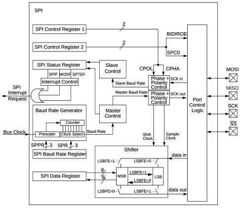
Figure 1-1 gives an overview on the SPI architecture. The main parts of the SPI are status,control and
data registers, shifter logic, baud rate generator, master/slave control logic and port control logic.
Figure 1-1 SPI Block Diagram
1.1 Overview
SPI Control Register 1
SPI Control Register 2
SPI Baud Rate Register SPI Status Register
SPI Data Register
Shifter Port Control Logic MOSI SCK Interrupt Control SPI MSB LSB LSBFE=1 LSBFE=0 LSBFE=0 LSBFE=1 data in LSBFE=1 LSBFE=0 data out 8 8 Baud Rate Generator
Prescaler
Bus Clock
Counter
Clock Select
SPPR 3 SPR 3
Baud Rate Phase + Polarity Control Master Slave SCK in SCK out Master Baud Rate
Slave Baud Rate
Phase + Polarity Control
Control
Control CPOL CPHA
2 BIDIROE SPC0 2 Shift Sample Clock Clock MODF SPIF SPTEF SPI Request Interrupt SS SPI Control Register 1
SPI Control Register 2
SPI Baud Rate Register SPI Status Register
SPI Data Register
Shifter Port Control Logic MOSI SCK Interrupt Control SPI MSB LSB LSBFE=1 LSBFE=0 LSBFE=0 LSBFE=1 data in LSBFE=1 LSBFE=0 data out 8 8 Baud Rate Generator
Prescaler
Bus Clock
Counter
Clock Select
SPPR 3 SPR 3
Baud Rate Phase + Polarity Control Master Slave SCK in SCK out Master Baud Rate
Slave Baud Rate
Phase + Polarity Control
Control
Control CPOL CPHA
1.2 Features
The SPI includes these distinctive features:
• Master mode and slave mode
• Bi-directional mode
• Slave select output
• Mode fault error flag with CPU interrupt capability
• Double-buffered data register
• Serial clock with programmable polarity and phase
• Control of SPI operation during wait mode
1.3 Modes of Operation
The SPI functions in three modes, run, wait, and stop.
• Run Mode
This is the basic mode of operation.
• Wait Mode
SPI operation in wait mode is a configurable low power mode, controlled by the SPISWAI bit located in the SPICR2 register. In wait mode, if the SPISWAI bit is clear, the SPI operates like in Run Mode. If the SPISWAI bit is set, the SPI goes into a power conservative state, with the SPI clock generation turned off. If the SPI is configured as a master, any transmission in progress stops, but is resumed after CPU goes into Run Mode. If the SPI is configured as a slave, reception and transmission of a byte continues, so that the slave stays synchronized to the master.
• Stop Mode
The SPI is inactive in stop mode for reduced power consumption. If the SPI is configured as a master, any transmission in progress stops, but is resumed after CPU goes into Run Mode. If the SPI is configured as a slave, reception and transmission of a byte continues, so that the slave stays synchronized to the master.
This is a high level description only, detailed descriptions of operating modes are contained in section4.8
Low Power Mode Options.
2.1 Overview
This section lists the name and description of all ports including inputs and outputs that do, or may, connect off chip. The SPI module has a total of 4 external pins.
2.2 Detailed Signal Description
2.2.1 MOSI
This pin is used to transmit data out of the SPI module when it is configured as a Master and receive data when it is configured as Slave.
2.2.2 MISO
This pin is used to transmit data out of the SPI module when it is configured as a Slave and receive data when it is configured as Master.
2.2.3 SS
This pin is used to output the select signal from the SPI module to another peripheral with which a data transfer is to take place when its configured as a Masterand its used as an input to receive the slave select signal when the SPI is configured as Slave.
2.2.4 SCK
This pin is used to output the clock with respect to which the SPI transfers data or receive clock in case of Slave.
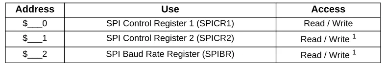
Section 3 Memory Map/Register Definition
This section provides a detailed description of address space and registers used by the SPI.
[image:15.612.109.504.625.690.2]The memory map for the SPI is given below inTable 3-1. The address listed for each register is the sum of a base address and an address offset. The base address is defined at the SoC level and the address offset is defined at the module level. Reads from the reserved bits return zeros and writes to the reserved bits have no effect.
Table 3-1 Module Memory Map
3.1 Register Descriptions
This section consists of register descriptions in address order. Each description includes a standard register diagram with an associated figure number. Details of register bit and field function follow the register diagrams, in bit order.
[image:16.612.116.502.70.191.2]3.1.1 SPI Control Register 1
Figure 3-1 SPI Control Register 1 (SPICR1)
Read: anytime Write: anytime
SPIE — SPI Interrupt Enable Bit
This bit enables SPI interrupt requests, if SPIF or MODF status flag is set. 1 = SPI interrupts enabled.
0 = SPI interrupts disabled.
SPE — SPI System Enable Bit
This bit enables the SPI system and dedicates the SPI port pins to SPI system functions. If SPE is cleared, SPI is disabled and forced into idle state, status bits in SPISR register are reseted
1 = SPI enabled, port pins are dedicated to SPI functions. 0 = SPI disabled (lower power consumption).
$___3 SPI Status Register (SPISR) Read2
$___4 Reserved —2 3
$___5 SPI Data Register (SPIDR) Read / Write
$___6 Reserved —2 3
$___7 Reserved —2 3
NOTES:
1. Certain bits are non-writable. 2. Writes to this register are ignored.
3. Reading from this register returns all zeros.
Register Address: $___0
Bit 7 6 5 4 3 2 1 Bit 0
R
SPIE SPE SPTIE MSTR CPOL CPHA SSOE LSBFE
W
[image:16.612.92.527.350.406.2]Reset: 0 0 0 0 0 1 0 0
0 = SPTEF interrupt disabled.
MSTR — SPI Master/Slave Mode Select Bit
This bit selects, if the SPI operates in master or slave mode. Switching the SPI from master to slave or vice versa forces the SPI system into idle state.
1 = SPI is in Master mode 0 = SPI is in Slave mode
CPOL — SPI Clock Polarity Bit
This bit selects an inverted or non-inverted SPI clock. To transmit data between SPI modules, the SPI modules must have identical CPOL values. In master mode, a change of this bit will abort a
transmission in progress and force the SPI system into idle state. 1 = Active-low clocks selected. In idle state SCK is high. 0 = Active-high clocks selected. In idle state SCK is low.
CPHA — SPI Clock Phase Bit
This bit is used to select the SPI clock format. In master mode, a change of this bit will abort a transmission in progress and force the SPI system into idle state.
1 = Sampling of data occurs at even edges (2,4,6,...,16) of the SCK clock 0 = Sampling of data occurs at odd edges (1,3,5,...,15) of the SCK clock
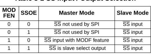
SSOE — Slave Select Output Enable
The SS output feature is enabled only in master mode, if MODFEN is set, by asserting the SSOE as shown inTable 3-2. In master mode, a change of this bit will abort a transmission in progress and force the SPI system into idle state.
LSBFE — LSB-First Enable
This bit does not affect the position of the MSB and LSB in the data register. Reads and writes of the data register always have the MSB in bit 7. In master mode, a change of this bit will abort a
transmission in progress and force the SPI system into idle state. 1 = Data is transferred least significant bit first.
[image:17.612.177.437.423.519.2]0 = Data is transferred most significant bit first.
Table 3-2 SS Input / Output Selection
MOD
FEN SSOE Master Mode Slave Mode
3.1.2 SPI Control Register 2
Figure 3-2 SPI Control Register 2 (SPICR2)
Read: anytime
Write: anytime; writes to the reserved bits have no effect
MODFEN — Mode Fault Enable Bit
This bit allows the MODF failure being detected. If the SPI is in Master mode and MODFEN is cleared, then the SS port pin is not used by the SPI. In Slave mode, the SS is available only as an input regardless of the value of MODFEN. For an overview on the impact of the MODFEN bit on the SS port pin configuration refer toTable 3-2. In master mode, a change of this bit will abort a transmission in progress and force the SPI system into idle state.
1 = SS port pin with MODF feature 0 = SS port pin is not used by the SPI
BIDIROE — Output enable in the Bidirectional mode of operation
This bit controls the MOSI and MISO output buffer of the SPI, when in bidirectional mode of operation (SPC0 is set). In master mode this bit controls the output buffer of the MOSI port, in slave mode it controls the output buffer of the MISO port. In master mode, with SPC0 set, a change of this bit will abort a transmission in progress and force the SPI into idle state.
1 = Output buffer enabled 0 = Output buffer disabled
SPISWAI — SPI Stop in Wait Mode Bit
This bit is used for power conservation while in wait mode. 1 = Stop SPI clock generation when in wait mode 0 = SPI clock operates normally in wait mode
SPC0 — Serial Pin Control Bit 0
This bit enables bidirectional pin configurations as shown inTable 3-3. In master mode, a change of this bit will abort a transmission in progress and force the SPI system into idle state
Register Address: $___1
Bit 7 6 5 4 3 2 1 Bit 0
R 0 0 0
MODFEN BIDIROE 0 SPISWAI SPC0 W
Reset: 0 0 0 0 0 0 0 0
3.1.3 SPI Baud Rate Register
Figure 3-3 SPI Baud Rate Register (SPIBR)
Read: anytime
Write: anytime; writes to the reserved bits have no effect
SPPR2–SPPR0 — SPI Baud Rate Preselection Bits
SPR2–SPR0 — SPI Baud Rate Selection Bits
These bits specify the SPI baud rates as shown in the table below. In master mode, a change of these bits will abort a transmission in progress and force the SPI system into idle state.
The baud rate divisor equation is as follows:
The baud rate can be calculated with the following equation:
Normal 0 X Master In Master Out
Bidirectional 1 0 MISO not used by SPI Master In
1 Master I/O
Slave Mode of Operation
Normal 0 X Slave Out SlaveIn
Bidirectional 1 0 Slave In MOSI not used by SPI
1 Slave I/O
Register Address: $___2
Bit 7 6 5 4 3 2 1 Bit 0
R 0
SPPR2 SPPR1 SPPR0 0 SPR2 SPR1 SPR0
W
Reset: 0 0 0 0 0 0 0 0
= Reserved
Table 3-3 Bidirectional Pin Configurations
Pin Mode SPC0 BIDIROE MISO MOSI
BaudRateDivisor = (SPPR+1)•2(SPR+1)
[image:19.612.87.525.251.336.2]0 0 0 0 0 1 4 6.25 MHz
0 0 0 0 1 0 8 3.125 MHz
0 0 0 0 1 1 16 1.5625 MHz
0 0 0 1 0 0 32 781.25 kHz
0 0 0 1 0 1 64 390.63 kHz
0 0 0 1 1 0 128 195.31 kHz
0 0 0 1 1 1 256 97.66 kHz
0 0 1 0 0 0 4 6.25 MHz
0 0 1 0 0 1 8 3.125 MHz
0 0 1 0 1 0 16 1.5625 MHz
0 0 1 0 1 1 32 781.25 kHz
0 0 1 1 0 0 64 390.63 kHz
0 0 1 1 0 1 128 195.31 kHz
0 0 1 1 1 0 256 97.66 kHz
0 0 1 1 1 1 512 48.83 kHz
0 1 0 0 0 0 6 4.16667 MHz
0 1 0 0 0 1 12 2.08333 MHz
0 1 0 0 1 0 24 1.04167 MHz
0 1 0 0 1 1 48 520.83 kHz
0 1 0 1 0 0 96 260.42 kHz
0 1 0 1 0 1 192 130.21 kHz
0 1 0 1 1 0 384 65.10 kHz
0 1 0 1 1 1 768 32.55 kHz
0 1 1 0 0 0 8 3.125 MHz
0 1 1 0 0 1 16 1.5625 MHz
0 1 1 0 1 0 32 781.25 kHz
0 1 1 0 1 1 64 390.63 kHz
0 1 1 1 0 0 128 195.31 kHz
0 1 1 1 0 1 256 97.66 kHz
0 1 1 1 1 0 512 48.83 kHz
0 1 1 1 1 1 1024 24.41 kHz
1 0 0 0 0 0 10 2.5 MHz
1 0 0 0 0 1 20 1.25 MHz
1 0 0 0 1 0 40 625 kHz
1 0 0 0 1 1 80 312.5 kHz
1 0 0 1 0 0 160 156.25 kHz
1 0 0 1 0 1 320 78.13 kHz
1 0 0 1 1 0 640 39.06 kHz
[image:20.612.89.522.65.715.2]1 0 0 1 1 1 1280 19.53 kHz
Table 3-4 Example SPI Baud Rate Selection (25 MHz Bus Clock)
NOTE: In slave mode of SPI S-clock speed DIV2 is not supported.
[image:21.612.98.518.71.382.2]3.1.4 SPI Status Register
Figure 3-4 SPI Status Register (SPISR)
Read: anytime Write: has no effect
1 0 1 1 0 0 192 130.21 kHz
1 0 1 1 0 1 384 65.10 kHz
1 0 1 1 1 0 768 32.55 kHz
1 0 1 1 1 1 1536 16.28 kHz
1 1 0 0 0 0 14 1.78571 MHz
1 1 0 0 0 1 28 892.86 kHz
1 1 0 0 1 0 56 446.43 kHz
1 1 0 0 1 1 112 223.21 kHz
1 1 0 1 0 0 224 111.61 kHz
1 1 0 1 0 1 448 55.80 kHz
1 1 0 1 1 0 896 27.90 kHz
1 1 0 1 1 1 1792 13.95 kHz
1 1 1 0 0 0 16 1.5625 MHz
1 1 1 0 0 1 32 781.25 kHz
1 1 1 0 1 0 64 390.63 kHz
1 1 1 0 1 1 128 195.31 kHz
1 1 1 1 0 0 256 97.66 kHz
1 1 1 1 0 1 512 48.83 kHz
1 1 1 1 1 0 1024 24.41 kHz
1 1 1 1 1 1 2048 12.21 kHz
Register Address: $___3
Bit 7 6 5 4 3 2 1 Bit 0
R SPIF 0 SPTEF MODF 0 0 0 0
W
Reset: 0 0 1 0 0 0 0 0
= Reserved
Table 3-4 Example SPI Baud Rate Selection (25 MHz Bus Clock)
[image:21.612.92.526.488.571.2]This bit is set after a received data byte has been transferred into the SPI Data Register. This bit is cleared by reading the SPISR register (with SPIF set) followed by a read access to the SPI Data Register.
1 = New data copied to SPIDR 0 = Transfer not yet complete
SPTEF — SPI Transmit Empty Interrupt Flag
If set, this bit indicates that the transmit data register is empty. To clear this bit and place data into the transmit data register, SPISR has to be read with SPTEF=1, followed by a write to SPIDR. Any write to the SPI Data Register without reading SPTEF=1, is effectively ignored.
1 = SPI Data register empty 0 = SPI Data register not empty
MODF — Mode Fault Flag
This bit is set if the SS input becomes low while the SPI is configured as a master and mode fault detection is enabled, MODFEN bit of SPICR2 register is set. Refer to MODFEN bit description in
3.1.2 SPI Control Register 2. The flag is cleared automatically by a read of the SPI Status Register
(with MODF set) followed by a write to the SPI Control Register 1. 1 = Mode fault has occurred.
0 = Mode fault has not occurred.
[image:22.612.94.529.392.457.2]3.1.5 SPI Data Register
Figure 3-5 SPI Data Register (SPIDR)
Read: anytime; normally read only after SPIF is set Write: anytime
The SPI Data Register is both the input and output register for SPI data. A write to this register allows a data byte to be queued and transmitted. For a SPI configured as a master, a queued data byte is transmitted immediately after the previous transmission has completed. The SPI Transmitter Empty Flag SPTEF in the SPISR register indicates when the SPI Data Register is ready to accept new data. Reading the data can occur anytime from after the SPIF is set to before the end of the next transfer. If the SPIF is not serviced by the end of the successive transfers, those data bytes are lost and the data within the SPIDR retains the first byte until SPIF is serviced.
Register Address: $___5
Bit 7 6 5 4 3 2 1 Bit 0
R
Bit 7 6 5 4 3 2 2 Bit 0
W
Section 4 Functional Description
4.1 General
The SPI module allows a duplex, synchronous, serial communication between the MCU and peripheral devices. Software can poll the SPI status flags or SPI operation can be interrupt driven.
The SPI system is enabled by setting the SPI enable (SPE) bit in SPI Control Register 1. While SPE bit is set, the four associated SPI port pins are dedicated to the SPI function as:
• Slave select (SS)
• Serial clock (SCK)
• Master out/slave in (MOSI)
• Master in/slave out (MISO)
The main element of the SPI system is the SPI Data Register. The 8-bit data register in the master and the 8-bit data register in the slave are linked by the MOSI and MISO pins to form a distributed 16-bit register. When a data transfer operation is performed, this 16-bit register is serially shifted eight bit positions by the S-clock from the master, so data is exchanged between the master and the slave. Data written to the master SPI Data Register becomes the output data for the slave, and data read from the master SPI Data Register after a transfer operation is the input data from the slave.
A read of SPISR with SPTEF=1 followed by a write to SPIDR puts data into the transmit data register. When a transfer is complete, received data is moved into the receive data register. Data may be read from this double-buffered system any time before the next transfer has completed. This 8-bit data register acts as the SPI receive data register for reads and as the SPI transmit data register for writes. A single SPI register address is used for reading data from the read data buffer and for writing data to the transmit data register.
The clock phase control bit (CPHA) and a clock polarity control bit (CPOL) in the SPI Control Register 1 (SPICR1) select one of four possible clock formats to be used by the SPI system. The CPOL bit simply selects a non-inverted or inverted clock. The CPHA bit is used to accommodate two fundamentally different protocols by sampling data on odd numbered SCK edges or on even numbered SCK edges (see
4.4 Transmission Formats).
The SPI can be configured to operate as a master or as a slave. When the MSTR bit in SPI Control Register1 is set, master mode is selected, when the MSTR bit is clear, slave mode is selected.
4.2 Master Mode
The SPR2, SPR1, and SPR0 baud rate selection bits in conjunction with the SPPR2, SPPR1, and SPPR0 baud rate preselection bits in the SPI Baud Rate register control the baud rate generator and determine the speed of the transmission. The SCK pin is the SPI clock output. Through the SCK pin, the baud rate generator of the master controls the shift register of the slave peripheral.
• MOSI, MISO pin
In master mode, the function of the serial data output pin (MOSI) and the serial data input pin (MISO) is determined by the SPC0 and BIDIROE control bits.
• SS pin
If MODFEN and SSOE bit are set, the SS pin is configured as slave select output. The SS output becomes low during each transmission and is high when the SPI is in idle state.
If MODFEN is set and SSOE is cleared, the SS pin is configured as input for detecting mode fault error. If the SS input becomes low this indicates a mode fault error where another master tries to drive the MOSI and SCK lines. In this case, the SPI immediately switches to slave mode, by clearing the MSTR bit and also disables the slave output buffer MISO (or SISO in bidirectional mode). So the result is that all outputs are disabled and SCK, MOSI and MISO are inputs. If a transmission is in progress when the mode fault occurs, the transmission is aborted and the SPI is forced into idle state.
This mode fault error also sets the mode fault (MODF) flag in the SPI Status Register (SPISR). If the SPI interrupt enable bit (SPIE) is set when the MODF flag gets set, then an SPI interrupt sequence is also requested.
When a write to the SPI Data Register in the master occurs, there is a half SCK-cycle delay. After the delay, SCK is started within the master. The rest of the transfer operation differs slightly, depending on the clock format specified by the SPI clock phase bit, CPHA, in SPI Control Register 1 (see 4.4
Transmission Formats).
NOTE: A change of the bits CPOL, CPHA, SSOE, LSBFE, MODFEN, SPC0, BIDIROE
with SPC0 set, SPPR2-SPPR0 and SPR2-SPR0 in master mode will abort a transmission in progress and force the SPI into idle state. The remote slave cannot detect this, therefore the master has to ensure that the remote slave is set back to idle state.
4.3 Slave Mode
The SPI operates in slave mode when the MSTR bit in SPI Control Register1 is clear.
• SCK clock
In slave mode, SCK is the SPI clock input from the master.
The SS pin is the slave select input. Before a data transmission occurs, the SS pin of the slave SPI must be low. SS must remain low until the transmission is complete. If SS goes high, the SPI is forced into idle state.
The SS input also controls the serial data output pin, if SS is high (not selected), the serial data output pin is high impedance, and, if SS is low the first bit in the SPI Data Register is driven out of the serial data output pin. Also, if the slave is not selected (SS is high), then the SCK input is ignored and no internal shifting of the SPI shift register takes place.
Although the SPI is capable of duplex operation, some SPI peripherals are capable of only receiving SPI data in a slave mode. For these simpler devices, there is no serial data out pin.
NOTE: When peripherals with duplex capability are used, take care not to simultaneously
enable two receivers whose serial outputs drive the same system slave’s serial data output line.
As long as no more than one slave device drives the system slave’s serial data output line, it is possible for several slaves to receive the same transmission from a master, although the master would not receive return information from all of the receiving slaves.
If the CPHA bit in SPI Control Register 1 is clear, odd numbered edges on the SCK input cause the data at the serial data input pin to be latched. Even numbered edges cause the value previously latched from the serial data input pin to shift into the LSB or MSB of the SPI shift register, depending on the LSBFE bit.
If the CPHA bit is set, even numbered edges on the SCK input cause the data at the serial data input pin to be latched. Odd numbered edges cause the value previously latched from the serial data input pin to shift into the LSB or MSB of the SPI shift register, depending on the LSBFE bit.
When CPHA is set, the first edge is used to get the first data bit onto the serial data output pin. When CPHA is clear and the SS input is low (slave selected), the first bit of the SPI data is driven out of the serial data output pin. After the eighth shift, the transfer is considered complete and the received data is transferred into the SPI Data Register. To indicate transfer is complete, the SPIF flag in the SPI Status Register is set.
NOTE: A change of the bits CPOL, CPHA, SSOE, LSBFE, MODFEN, SPC0 and BIDIROE
with SPC0 set in slave mode will corrupt a transmission in progress and has to be avoided.
4.4 Transmission Formats
Figure 4-1 Master/Slave Transfer Block Diagram
4.4.1 Clock Phase and Polarity Controls
Using two bits in the SPI Control Register1, software selects one of four combinations of serial clock phase and polarity.
The CPOL clock polarity control bit specifies an active high or low clock and has no significant effect on the transmission format.
The CPHA clock phase control bit selects one of two fundamentally different transmission formats.
Clock phase and polarity should be identical for the master SPI device and the communicating slave device. In some cases, the phase and polarity are changed between transmissions to allow a master device to communicate with peripheral slaves having different requirements.
4.4.2 CPHA = 0 Transfer Format
The first edge on the SCK line is used to clock the first data bit of the slave into the master and the first data bit of the master into the slave. In some peripherals, the first bit of the slave’s data is available at the slave’s data out pin as soon as the slave is selected. In this format, the first SCK edge is issued a half cycle after SS has become low.
A half SCK cycle later, the second edge appears on the SCK line. When this second edge occurs, the value previously latched from the serial data input pin is shifted into the LSB or MSB of the shift register, depending on LSBFE bit.
After this second edge, the next bit of the SPI master data is transmitted out of the serial data output pin of the master to the serial input pin on the slave. This process continues for a total of 16 edges on the SCK line, with data being latched on odd numbered edges and shifted on even numbered edges.
SHIFT REGISTER
SHIFT REGISTER
BAUD RATE GENERATOR
MASTER SPI SLAVE SPI
MOSI MOSI
MISO MISO
SCK SCK
SS SS
• Data that was previously in the master SPI Data Register should now be in the slave data register and the data that was in the slave data register should be in the master.
[image:27.612.79.535.204.520.2]• The SPIF flag in the SPI Status Register is set indicating that the transfer is complete.
Figure 4-2is a timing diagram of an SPI transfer where CPHA = 0. SCK waveforms are shown for CPOL
= 0 and CPOL = 1. The diagram may be interpreted as a master or slave timing diagram since the SCK, MISO, and MOSI pins are connected directly between the master and the slave. The MISO signal is the output from the slave and the MOSI signal is the output from the master. The SS pin of the master must be either high or reconfigured as a general-purpose output not affecting the SPI.
Figure 4-2 SPI Clock Format 0 (CPHA = 0)
In slave mode, if the SS line is not deasserted between the successive transmissions then the content of the SPI Data Register is not transmitted, instead the last received byte is transmitted. If the SS line is
deasserted for at least minimum idle time ( half SCK cycle) between successive transmissions then the
tL
Begin End
SCK (CPOL = 0)
SAMPLE I
CHANGE O
SEL SS (O)
Transfer
SCK (CPOL = 1)
MSB first (LSBFE = 0): LSB first (LSBFE = 1):
MSB LSB LSB MSB Bit 5 Bit 2 Bit 6 Bit 1 Bit 4 Bit 3 Bit 3 Bit 4 Bit 2 Bit 5 Bit 1 Bit 6 CHANGE O
SEL SS (I) MOSI pin MISO pin Master only MOSI/MISO tT If ne xt tr ansf
er begins here
for tT, tl, tL Minimum 1/2 SCK
tI tL
tL = Minimum leading time before the first SCK edge
tT = Minimum trailing time after the last SCK edge
tI = Minimum idling time between transfers (minimum SS high time)
tL, tT, and tI are guaranteed for the master mode and required for the slave mode.
1 2 3 4 5 6 7 8 9 10 11 12 13 14 15 16 SCK Edge Nr.
4.4.3 CPHA = 1 Transfer Format
Some peripherals require the first SCK edge before the first data bit becomes available at the data out pin, the second edge clocks data into the system. In this format, the first SCK edge is issued by setting the CPHA bit at the beginning of the 8-cycle transfer operation.
The first edge of SCK occurs immediately after the half SCK clock cycle synchronization delay. This first edge commands the slave to transfer its first data bit to the serial data input pin of the master.
A half SCK cycle later, the second edge appears on the SCK pin. This is the latching edge for both the master and slave.
When the third edge occurs, the value previously latched from the serial data input pin is shifted into the LSB or MSB of the SPI shift register, depending on LSBFE bit. After this edge, the next bit of the master data is coupled out of the serial data output pin of the master to the serial input pin on the slave.
This process continues for a total of 16 edges on the SCK line with data being latched on even numbered edges and shifting taking place on odd numbered edges.
Data reception is double buffered, data is serially shifted into the SPI shift register during the transfer and is transferred to the parallel SPI Data Register after the last bit is shifted in.
After the 16th SCK edge:
• Data that was previously in the SPI Data Register of the master is now in the data register of the slave, and data that was in the data register of the slave is in the master.
• The SPIF flag bit in SPISR is set indicating that the transfer is complete.
Figure 4-3shows two clocking variations for CPHA = 1. The diagram may be interpreted as a master or
slave timing diagram since the SCK, MISO, and MOSI pins are connected directly between the master and the slave. The MISO signal is the output from the slave, and the MOSI signal is the output from the master. The SS line is the slave select input to the slave. The SS pin of the master must be either high or
Figure 4-3 SPI Clock Format 1 (CPHA = 1)
The SS line can remain active low between successive transfers (can be tied low at all times). This format is sometimes preferred in systems having a single fixed master and a single slave that drive the MISO data line.
• Back to Back transfers in master mode
In master mode, if a transmission has completed and a new data byte is available in the SPI Data Register, this byte is send out immediately without a trailing and minimum idle time.
The SPI interrupt request flag (SPIF) is common to both the master and slave modes. SPIF gets set one half SCK cycle after the last SCK edge.
4.5 SPI Baud Rate Generation
tL tT
for tT, tl, tL Minimum 1/2 SCK
tI tL
If ne
xt tr
ansf
er begins here
Begin End
SCK (CPOL = 0)
SAMPLE I
CHANGE O
SEL SS (O)
Transfer
SCK (CPOL = 1)
MSB first (LSBFE = 0): LSB first (LSBFE = 1):
MSB LSB LSB MSB Bit 5 Bit 2 Bit 6 Bit 1 Bit 4 Bit 3 Bit 3 Bit 4 Bit 2 Bit 5 Bit 1 Bit 6 CHANGE O
SEL SS (I) MOSI pin
MISO pin
Master only MOSI/MISO
tL = Minimum leading time before the first SCK edge, not required for back to back transfers tT = Minimum trailing time after the last SCK edge
tI = Minimum idling time between transfers (minimum SS high time), not required for back to back transfers 1 2 3 4 5 6 7 8 9 10 11 12 13 14 15 16 SCK Edge Nr.
The SPI clock rate is determined by the product of the value in the baud rate preselection bits
(SPPR2–SPPR0) and the value in the baud rate selection bits (SPR2–SPR0). The module clock divisor equation is shown inFigure 4-4.
When all bits are clear (the default condition), the SPI module clock is divided by 2. When the selection bits (SPR2–SPR0) are 001 and the preselection bits (SPPR2–SPPR0) are 000, the module clock divisor becomes 4. When the selection bits are 010, the module clock divisor becomes 8 etc.
When the preselection bits are 001, the divisor determined by the selection bits is multiplied by 2. When the preselection bits are 010, the divisor is multiplied by 3, etc. SeeTable 3-4for baud rate calculations for all bit conditions, based on a 25 MHz Bus Clock. The two sets of selects allows the clock to be divided by a non-power of two to achieve other baud rates such as divide by 6, divide by 10, etc.
The baud rate generator is activated only when the SPI is in the master mode and a serial transfer is taking place. In the other cases, the divider is disabled to decrease IDD current.
Figure 4-4 Baud Rate Divisor Equation
4.6 Special Features
4.6.1 SS Output
The SS output feature automatically drives the SS pin low during transmission to select external devices and drives it high during idle to deselect external devices. When SS output is selected, the SS output pin is connected to the SS input pin of the external device.
The SS output is available only in master mode during normal SPI operation by asserting SSOE and MODFEN bit as shown inTable 3-2.
The mode fault feature is disabled while SS output is enabled.
NOTE: Care must be taken when using the SS output feature in a multimaster system since
the mode fault feature is not available for detecting system errors between masters.
4.6.2 Bidirectional Mode (MOMI or SISO)
The bidirectional mode is selected when the SPC0 bit is set in SPI Control Register 2 (see Table 4-1
Normal Mode and Bidirectional Mode). In this mode, the SPI uses only one serial data pin for the
interface with external device(s). The MSTR bit decides which pin to use. The MOSI pin becomes the serial data I/O (MOMI) pin for the master mode, and the MISO pin becomes serial data I/O (SISO) pin for
The direction of each serial I/O pin depends on the BIDIROE bit. If the pin is configured as an output, serial data from the shift register is driven out on the pin. The same pin is also the serial input to the shift register.
The SCK is output for the master mode and input for the slave mode.
The SS is the input or output for the master mode, and it is always the input for the slave mode.
The bidirectional mode does not affect SCK and SS functions.
NOTE: In bidirectional master mode, with mode fault enabled, both data pins MISO and
MOSI can be occupied by the SPI, though MOSI is normally used for transmissions in bidirectional mode and MISO is not used by the SPI. If a mode fault occurs, the SPI is automatically switched to slave mode, in this case MISO becomes occupied by the SPI and MOSI is not used. This has to be considered, if the MISO pin is used for other purpose.
4.7 Error Conditions
The SPI has one error condition:
• Mode fault error
[image:31.612.69.545.70.314.2]4.7.1 Mode Fault Error
Table 4-1 Normal Mode and Bidirectional Mode
When SPE = 1 Master Mode MSTR = 1 Slave Mode MSTR = 0
Normal Mode SPC0 = 0
Bidirectional Mode SPC0 = 1
permitted in normal operation, the MODF bit in the SPI Status Register is set automatically provided the MODFEN bit is set.
In the special case where the SPI is in master mode and MODFEN bit is cleared, the SS pin is not used by the SPI. In this special case, the mode fault error function is inhibited and MODF remains cleared. In case the SPI system is configured as a slave, the SS pin is a dedicated input pin. Mode fault error doesn’t occur in slave mode.
If a mode fault error occurs the SPI is switched to slave mode, with the exception that the slave output buffer is disabled. So SCK, MISO and MOSI pins are forced to be high impedance inputs to avoid any possibility of conflict with another output driver. A transmission in progress is aborted and the SPI is forced into idle state.
If the mode fault error occurs in the bidirectional mode for a SPI system configured in master mode, output enable of the MOMI (MOSI in bidirectional mode) is cleared if it was set. No mode fault error occurs in the bidirectional mode for SPI system configured in slave mode.
The mode fault flag is cleared automatically by a read of the SPI Status Register (with MODF set) followed by a write to SPI Control Register 1. If the mode fault flag is cleared, the SPI becomes a normal master or slave again.
4.8 Low Power Mode Options
4.8.1 SPI in Run Mode
In run mode with the SPI system enable (SPE) bit in the SPI control register clear, the SPI system is in a low-power, disabled state. SPI registers can still be accessed, but clocks to the core of this module are disabled.
4.8.2 SPI in Wait Mode
SPI operation in wait mode depends upon the state of the SPISWAI bit in SPI Control Register 2.
• If SPISWAI is clear, the SPI operates normally when the CPU is in wait mode
• If SPISWAI is set, SPI clock generation ceases and the SPI module enters a power conservation state when the CPU is in wait mode.
– If SPISWAI is set and the SPI is configured for master, any transmission and reception in progress stops at wait mode entry. The transmission and reception resumes when the SPI exits wait mode.
If the master transmits several bytes while the slave is in wait mode, the slave will continue to send out bytes consistent with the operation mode at the start of wait mode (i.e. If the slave is currently sending its SPIDR to the master, it will continue to send the same byte. Else if the slave is currently sending the last received byte from the master, it will continue to send each previous master byte).
NOTE: Care must be taken when expecting data from a master while the slave is in wait or
stop mode. Even though the shift register will continue to operate, the rest of the SPI is shut down (i.e. a SPIF interrupt will not be generated until exiting stop or wait mode). Also, the byte from the shift register will not be copied into the SPIDR register until after the slave SPI has exited wait or stop mode. A SPIF flag and SPIDR copy is only generated if wait mode is entered or exited during a
tranmission. If the slave enters wait mode in idle mode and exits wait mode in idle mode, neither a SPIF nor a SPIDR copy will occur.
4.8.3 SPI in Stop Mode
Stop mode is dependent on the system. The SPI enters stop mode when the module clock is disabled (held high or low). If the SPI is in master mode and exchanging data when the CPU enters stop mode, the transmission is frozen until the CPU exits stop mode. After stop, data to and from the external SPI is exchanged correctly. In slave mode, the SPI will stay synchronized with the master.
The stop mode is not dependent on the SPISWAI bit.
4.8.4 Reset
The reset values of registers and signals are described in the Memory Map and Registers section (see
Section 3 Memory Map/Register Definition) which details the registers and their bit-fields.
• If a data transmission occurs in slave mode after reset without a write to SPIDR, it will transmit garbage, or the byte last received from the master before the reset.
• Reading from the SPIDR after reset will always read a byte of zeros.
4.8.5 Interrupts
The SPI only originates interrupt requests when SPI is enabled (SPE bit in SPICR1 set). The following is a description of how the SPI makes a request and how the MCU should acknowledge that request. The interrupt vector offset and interrupt priority are chip dependent.
The interrupt flags MODF, SPIF and SPTEF are logically ORed to generate an interrupt request.
• MSTR=0, The master bit in SPICR1 resets.
The MODF interrupt is reflected in the status register MODF flag. Clearing the flag will also clear the interrupt. This interrupt will stay active while the MODF flag is set. MODF has an automatic clearing process which is described in3.1.4 SPI Status Register.
4.8.5.2 SPIF
SPIF occurs when new data has been received and copied to the SPI Data Register. Once SPIF is set, it does not clear until it is serviced. SPIF has an automatic clearing process which is described in3.1.4 SPI
Status Register. In the event that the SPIF is not serviced before the end of the next transfer (i.e. SPIF
remains active throughout another transfer), the latter transfers will be ignored and no new data will be copied into the SPIDR.
4.8.5.3 SPTEF
SPTEF occurs when the SPI Data Register is ready to accept new dataOnce SPTEF is set, it does not clear until it is serviced. SPTEF has an automatic clearing process which is described in3.1.4 SPI Status
Register.
Index
–B–
Block diagram 13
–C–
Cross reference 13
–D–
Diagram block 13
–F–
Figure
cross-reference style 13
–I–
Initialization/application information 34
–S–