current-driven spin dynamics in
magnetic tunnel junctions
by
Mario Galante
A thesis submitted in partial fulfillment for the
degree of Doctor of Philosophy in the
School of Physics, Trinity College Dublin
I declare that this thesis has not been submitted as an exercise for a degree at this
or any other university and it is entirely my own work. I was involved in a number
of collaborations, and where it is appropriate my collaborators are acknowledged for
their contributions.
I agree to deposit this thesis in the University’s open access institutional
reposi-tory or allow the library to do so on my behalf, subject to Irish Copyright Legislation
and Trinity College Library conditions of use and acknowledgement.
Magnetic materials are of fundamental importance for the next generation of sensing
and storage applications. The operating principle of such devices is based upon
manipulating the orientation of the atomic magnetic moments. The dynamics of the
latter can be efficiently driven through the injection of spin-polarised currents that
generate effective torques, by spin conservation. These are commonly known as spin
torques. State-of-the-art devices employ two ferromagnets sandwiching an insulating
spacer, i.e. a magnetic tunnel junction, where information is stored in the mutual
orientation of the two magnetisations. These structures are engineered so that the
magnetisation vector of one magnetic layer is kept fixed along a given direction, while
the magnetisation of the other ferromagnet, also known as free layer, can be reversed
with an electric current. The elevated sensitivity of the magnetisation switching to
factors such as the properties of the ferromagnet, the quality of the interfaces and
temperature fluctuations makes the search of novel materials for these applications a
troublesome task. Here we present a multi-scale study of the magnetisation switching
in Fe/MgO-based magnetic tunnel junctions for different compositions of the free
magnetic layer. We begin by investigating the atom-dependence of the spin torques
with the objective of determining the factors that define their materials dependence.
This is done by the means of quantum transport calculations performed with a
combination of non-equilibrium Green’s functions and density functional theory. The
calculated spin torques are then used as input for spin dynamics simulations at the
atomistic scale, in order to compare the current-driven magnetisation switching in the
the spin torques for a given free layer can be predicted from the band structure of the
ferromagnet. However, in many cases the presence of additional interfaces or
non-uniform magnetic textures drastically modifies the predicted profile. Nevertheless,
the details of the decay of the spin torques do not imply significant modifications of
the switching properties. In fact, we find that the critical voltage required to obtain
magnetisation reversal is essentially dictated by the total torque acting on the free
layer. We continue with a study of antiferromagnetism in the Mn3Ga and Fe2MnGa Heusler compounds, in which magnetic properties are dominated by the moments
at the Mn sites. Antiferromagnetic materials are of great interest for spintronic
applications, since they may push the spin dynamics in the THz range, as opposed
to the GHz range of the one in ferromagnets. Our results show that the spin model
for Mn3Ga displays an extremely high-frequency oscillation mode, which is found to be characteristic of this system. In contrast, we find that the induced moments at
the Fe sites in Fe2MnGa are extremely sensitive to the presence of interfaces and to the alignment of the neighbouring Mn atoms. This is observed through both spin
dynamics simulations and first principles quantum transport calculations. Finally,
we derive a novel parameter-free method for the estimation of the Gilbert damping
None of this work would have been possible without the support of many people.
First and foremost, I would like to express my deepest gratitude to my supervisor,
Prof. Stefano Sanvito, for his guidance, teachings and patience. His great curiosity
and passion for science have been an inspiration and it has been a privilege to work
under his supervision. Secondly, I am grateful to all my colleagues, past and present,
in the Computational Spintronics Group for their support. Special thanks are due
to Dr. Matthew Ellis, who generously shared his computer code and experience on
atomistic spin dynamics and without whom large part of this thesis would not have
been possible. He has been been incredibly patient and helpful for the entire four
years, and he has always been there to lend his advice, both at a professional and a
personal level, despite his numerous other commitments. A second round of special
thanks goes to Emanuele Bosoni, Dr. Alessandro Lunghi and James Nelson
(collec-tively known as the B. F. ) for their friendship. Emanuele was a great companion
since my very first week in Dublin and a wonderful friend along the way, while I will
always be indebted to Alessandro for generously sharing his pearls of wisdom and
tips on both private and professional life. I am also very grateful to Dr. Mario ˘Zic,
Dr. Subhayan Roychouduri, Dr. Rajarshi Tiwari, Dr. Aswhinee Kumar, Anais
Col-ibaba, Urvesh Patil and Dr. Stella Skiadopoulou for their companionship. Finally, I
would like to thank Stefania Negro for her generous support in many administrative
and financial matters.
I would like to thank the Science Foundation of Ireland (Grants No. 14/IA/2624
support for attending conferences. I also acknowledge TCHPC (Research IT, Trinity
College Dublin) and the Irish Center for High-End Computing (ICHEC) for the
provision of computational facilities and assistance.
I also would like to thank all the other friends that I made in Dublin, who made
my stay here most enjoyable. Janne Shoening, for her company around the many
trips around Ireland. `Elia Cantoni i G`omez, for being an excellent jogging partner
and an irreplaceable friend. Dr. Silvia Fogli, for her support in the last few months
and for sharing her father’s boar meat. Finally, I am greatful to my flatmates, Maria
Pilar Guerola Fuentes, Christina Clarke and Rachel Cregan for their support, with
a special mention to Maria for her great friendship during these years.
Last but not least, I would like to thank all my family who always supported me
during my studies. Special mention goes to my parents and to my uncles Marco and
Abstract i
Acknowledgements iii
Contents v
List of Figures xxi
1 Magnetic random access memories 1
1.1 The development of STT-MRAMs . . . 3
1.1.1 Giant magnetoresistance and the advent of spintronics . . . . 3
1.1.2 Magnetic tunnelling junctions . . . 6
1.1.3 Spin transfer torque random access memories . . . 10
1.2 Designing magnetic tunnel junctions for high-performance memories . 14
1.2.1 Current challenges and perspectives . . . 20
1.3 Summary and thesis overview . . . 21
2 Ground-state and transport properties of magnetic materials 25
2.1 Electronic structure theory . . . 27
2.1.1 Model Hamiltonians . . . 28
2.1.2 Density functional theory and the Kohn-Sham problem . . . . 31
2.1.2.1 Spin density functional theory . . . 36
2.1.2.2 Constrained density functional theory . . . 38
2.1.3.1 Pseudopotentials and relativistic corrections . . . 40
2.1.3.2 Basis set . . . 43
2.1.3.3 Kohn-Sham Hamiltonian. . . 45
2.1.4 Summary . . . 47
2.2 Green’s function method for electronic transport . . . 47
2.2.1 Non-equilibrium Green’s functions theory . . . 51
2.2.1.1 Green’s functions and self-energies on the Keldysh contour . . . 54
2.2.1.2 Lesser, greater, retarded and advanced Green’s func-tions . . . 56
2.2.2 The SMEAGOL code . . . 60
2.2.2.1 Leads self-energies . . . 61
2.2.2.2 Out-of-equilibrium density matrix. . . 63
2.2.2.3 Electric current and transmission . . . 65
2.2.2.4 Self-consistency and influence of the bias voltage . . 68
2.2.3 Summary . . . 70
3 Spin torques in Fe/MgO-based magnetic tunnel junctions 73 3.1 Spin transfer torques: a theoretical overview . . . 75
3.1.1 Going from the continuum scale to ab-initio modelling . . . . 79
3.2 The Fe/MgO/Fe junction . . . 83
3.3 Disorder at the Fe/MgO interface . . . 90
3.4 Material dependence of the spin torques . . . 96
3.4.1 The influence of induced magnetic moments in L10-FePt . . . 101
3.5 Conclusions . . . 108
4 Current-driven atomistic spin dynamics 109 4.1 Modelling the dynamical properties of atomistic spins . . . 110
4.1.1 Parameterising the spin Hamiltonian . . . 115
4.1.1.1 Inter-atomic exchanges . . . 115
4.2 Spin Hamiltonian for ferromagnetic materials . . . 121
4.2.1 bcc Fe . . . 121
4.2.2 The inclusion of longitudinal spin fluctuations . . . 126
4.3 Spin-torque driven dynamics in Fe/MgO-based junctions . . . 130
4.3.1 Fe: different leads . . . 133
4.3.2 Disordered Fe/MgO/Fe . . . 141
4.3.3 L10 FePt . . . 143
4.4 Conclusions . . . 149
5 Antiferromagnetic couplings in Heusler compounds 151 5.1 Ferrimagnetism in Mn3Ga . . . 152
5.2 Multi-scale modelling of Fe2MnGa . . . 157
5.2.1 Atomistic model . . . 160
5.2.2 Spin transport. . . 163
5.3 Conclusions . . . 169
6 Parameter-free modelling of magnetic damping 171 6.1 Spin relaxation time and Gilbert damping . . . 174
6.2 Density functional theory method for spin relaxation time calculations 176 6.3 Summary . . . 181
7 Conclusions and future work 183
A List of publications 187
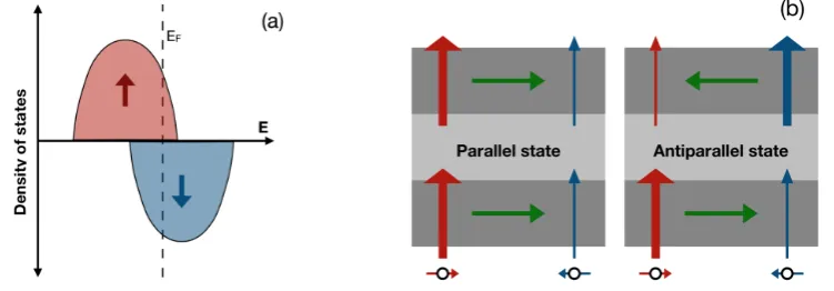
1.1 (a) Graphic representation of the density of states of a ferromagnet
around the Fermi energy. (b) Schematic illustration of the GMR effect.
The green arrows represent the orientation of the magnetisation
vec-tors, while red (blue) arrows represent the intensity of the transmission
for the majority (minority) spin channel. For parallel magnetisations
(left) the conductivity is enhanced for one spin channel and suppressed
for the other, so that the short-circuit through the former channel
im-plies a reduced resistance. On the contrary, in the anti-parallel state
(right) the two spin channels have the same conductivity, hence the
resistance is higher compared to the parallel magnetisation state. . . 5
1.2 Schematic of the difference tunnelling properties in crystalline MgO
and amorphous Al2O3 barriers. In Fe/MgO/Fe tunnelling is enhanced
for electrons of a ∆1 symmetry state, while Bloch state symmetries do
not play a role in the determination of tunnelling probabilities across
amorphous barriers. . . 8
1.3 Comparison between the real (a) and complex (b) band structure of
MgO and the majority (c) and minority (d) spin real band structure
1.4 Schematic representation of the mechanism that gives rise to a
spin-transfer torque in an MTJ. If an electric current is flowing from left
to right, it enters the free (right hand side) layer with the spin
polar-isation of the reference (left hand side) magnetic layer. The exchange
interaction causes electrons emerging from the barrier to adapt their
spins to the static local magnetisation,MF ree, thus transferring
angu-lar momentum to the free layer. As a result of spin conservation, the
local magnetisation vector is driven to align with the spin polarisation
of the current, i.e. it experiences an effective spin torque. . . 11
1.5 Schematic representation of current-driven magnetisation dynamics.
The field-like torque and the interaction with the effective field, Heff,
induce a precession around Heff, while the spin-transfer torque and
damping effects control the alignment between the magnetisation
vec-tor, m, and Heff. . . 13
1.6 Typical multilayered stack including a magnetic tunnel junction with
an in-plane magnetisation geometry for STT-MRAM applications. . 16
1.7 Typical multilayered stack including a magnetic tunnel junction with
a perpendicular-to-plane magnetisation geometry for STT-MRAM
ap-plications. . . 19
2.1 (a) Pseudo-wavefunction and all-electron wavefunction for the Fe-4s
shell and (b) corresponding pseudopotential. . . 42
2.2 Schematics of a two-terminal device. A lead can be represented by
a semi-infinite series of blocks described by Hamiltonians, H0, each
interacting only with adjacent blocks via the coupling matrix, H1
(H−1 = H
†
1). The extended molecule is described by the
Hamilto-nian, HM, and with the first block of the left- (right-) hand side lead
through, HM L (HM R), with HLM =H †
M L (HRM =H †
2.3 Graphical representation of the Keldysh path as divided into two
seg-ments, γ±, with its orientation is given by the light blue arrows. The
contour starts at timet0 in the upper complex semiplane, it continues
to +∞ to then return to t0 from the lower complex semiplane. The
position of a generic timet ≥t0 on the contour is also depicted.
Quan-tities evaluated at equivalent times that belong to different segments
assume by definition the same value, hence the contour is a closed line. 54
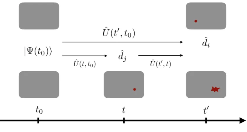
2.4 Graphic representation of the two states obtained through the different
evolution patterns considered in Eq. (2.65). In the evolution path
considered in the top of the figure the final state is obtained through
the destruction of a particle in the state i at a time, t0, represented by the red circle. On the contrary, the evolution pattern shown at
the bottom is obtained by destroying a particle in the state j at an
intermediate time,t0 < t < t0. The resulting state is then evolved until
the final time, t0, and the “spreading”of the absence of the particle state with quantum number j is represented with the irregular red
shape in the bottom right figure. . . 57
3.1 Setup for a spin torque calculation of a Fe/MgO/Fe junction. The
different color of the spheres correspond to different atomic species:
red for Fe, blue for Mg and green for O. The green arrows represent
the magnetisation of the two magnetic layers. . . 83
3.2 Panel (a) : majority (left panel) and minority (right panel) spin
trans-mission coefficients at the Fermi energy plotted over the 2D Brillouin
zone in Fe/MgO/Fe for parallel (P) magnetisations. The colored scale
indicates the intensity of the coefficient at a given k-vector (in
loga-rithmic scale), with Γ positioned at the centre of each square. Panel
(b) : current density for different voltage in Fe/MgO/Fe for parallel
3.3 In-plane [panel (a)] and out-of-plane [panel (b)] components of the
torkance in Fe/MgO/Fe in the zero-bias limit (black squares) and for
a bias voltage of 0.5 V (blue circles). These results were obtained for
an angleϑ=π/2 between the magnetisations of the reference and free
layer. . . 88
3.4 Bias dependence of the out-of-plane (a) and in-plane (b) component of
the spin torque in Fe/MgO/Fe integrated over the free layer. The spin
density method (DM) presented in the previous section is compared
to the prediction obtained by the means of conservation of the spin
current (CM) and within the Slonczewski model (S). . . 89
3.5 Schematic representation of the cell adopted to simulate a disordered
barrier. The total cross section is divided into a number of different
regions in which the spin currents flow independently (in parallel).
This allows us to combine the results of spin torque calculations with
different barriers and characterise the spin torques on a larger system. 90
3.6 Comparison of the in-plane torkance in Fe/MgO/Fe for barriers formed
by 4,5,6 and 7 MgO MLs. Panel (a) shows the in-plane torkances
summed over the free layer. The line is the result of our best fit to
the function aexp(−b∗x), with a = 787116 in the units of torkance
and b = 1.61864. Panel (b) contains the spatial distribution of the
normalised in-plane torkance at the insulator/metal interface. . . 91
3.7 Oxidised interface as considered in the supercell calculations. The
different color of the spheres corresponds to different atomic species:
red for Fe, blue for Mg and green for O. The scheme on the right-hand
side shows the notation adopted to identify each unit cell in the cross
section. We define the origin of the cartesian axes as the origin for the
oxidised cell, hereon also denoted as (0,0). The remaining unit cells
are then identified according to the position of their origin in units of
3.8 Results of transport calculations on Fe/MgO/Fe MTJs with a clean
(blue squares/lines) and a 25% oxidised (red circles/lines)
insula-tor/free layer interface. Left: planar average of the atomic
mag-netic moments in proximity of the interface (centered at 0). Right:
energy-dependent transmission coefficients for majority- (full lines)
and minority-spin (dashed lines). . . 94
3.9 Calculated torkance per unit ofµB/2 and area in a Fe/MgO/FeO0.25/Fe
junction. Each panel corresponds to a different region of the 2x2
su-percell, where and the two vertical dashed lines indicate the position of
the MgO/FeO0.25and FeO0.25/Fe interfaces. The colored background
indicates the atomic species: blue for O, green for Mg and red for Fe. 95
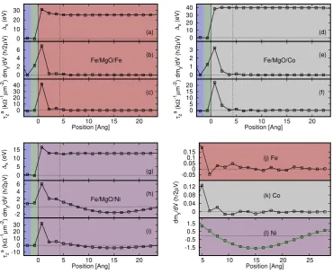
3.10 Study of the torkance in free layers composed by Fe (top left panel),
Co (top right panel), Ni (bottom left panel). In all the panels the
colored background indicates the atomic species: blue for O, green
for Mg, red for Fe, light grey for Co, violet for Ni. The top left, top
right and bottom left figures display the relevant components of [(a),
(d), (g)] the exchange and correlation field, ∆, [(b), (e), (h)] the
non-equilibrium spin density, dm/dV, and [(c), (f), (i)] the torkance per
unit of µB/2 and area, τ. The bottom right figure shows the details
of the decay of the non-equilibrium spin density in (j) Fe, (k) Co and
(l) Ni beyond the position indicated by the dashed vertical line in the
other figures (note the different scales). The green line in panel (l)
represents the best fit of the function in Eq. (3.23) to the underlying
data. . . 96
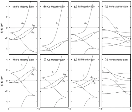
3.11 Band structure of, from left to right, Fe, Co, Ni and FePt for majority
(top panels) and minority (bottom panels) spins fork-vectors parallel
to the transport direction. For all materials the in-plane lattice
pa-rameter is that of the junction, i.e. of bcc Fe, and the structures for
Fe, Co and Ni are all bcc. The production of the data contained in
3.12 Study of the torkance acting on Fe/MgO/Fe/Cu (left) and Fe/MgO/Ni/Cu
(right). The colored background indicates the different atomic species:
blue for O, green for Mg, red for Fe, purple for Ni and orange for Cu.
The top panels display the relevant components of the exchange and
correlation field, ∆x, the middle panels the non-equilibrium spin
den-sity, dmy/dV, and the bottom panels the torkance per unit of µB/e
and area, τz. . . 100
3.13 Left: unit cell of L10 FePt with red (gray) spheres representing Fe
(Pt) atoms. Right: comparison of the energy dependent transmission
coefficients for majority (full lines) and minority (dashed lines) for
junctions with FePt (red), Fe (blue) and FePt/Fe (green) free layers. 103
3.14 Study of the torkance in a FePt free layer in the case of the
unre-alistically underestimated (left) and the realistic (right) MgO-FePt
inter-plane distance. The coloured background indicates the atomic
species: blue for O, green for Mg, red for Fe, grey for Pt. The relevant
components of (a), (d) the exchange and correlation field,∆, (b), (e)
the non-equilibrium spin density, dm/dV, and (c), (f) the torkance
per unit of µB/e and area, τ. . . 103
3.15 Study of the torkance in a FePt/Fe free layer. The coloured
back-ground indicates the atomic species: red for Fe, grey for Pt, blue for
O, green for Mg. Left panel: the relevant components of (a) the
ex-change and correlation field, ∆, (b) the non-equilibrium spin density,
dm/dV, and (c) the torkance per unit of µB/e and area, τ. Data
points represent by black squares are the results of a non-relativistic
calculation, while blue circles represent results of a calculation
3.16 Study of the torkance in a Fe/FePt/Fe free layer. In both sub figures
the coloured background indicates the atomic species: red for Fe, grey
for Pt, blue for O, green for Mg. Left panel: the relevant components
of (a) the exchange and correlation field,∆, (b) the non-equilibrium
spin density, dm/dV, and (c) the torkance per unit ofµB/eand area,
τ. Black squares and blue circles indicate results obtained without and
with relativistic corrections, respectively. Right Panel: comparison of
the torkance per unit µB/e and area of MTJs with (d) 1, (e) 2, (f) 3
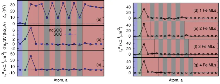
and (g) 4 Fe MLs as seed layer. . . 106
3.17 Study of the torkance in a Ni/FePt/Fe free layer made of 4 FePt
monolayers and a variable number of Fe monolayers inserted between
MgO and FePt. Left panel: the relevant components of (a) the
ex-change and correlation field, ∆, (b) the non-equilibrium spin density,
dm/dV and (c) the torkance per unit of µB/e and area, τ. Black
squares and blue circles indicate results obtained without and with
relativistic corrections, respectively. Right Panel: comparison of the
torkance per unitµB/eand area of MTJs with with a seed layer
com-prising (d) 1, (e) 2, 3 (f) and 4 (g) Fe monolayers. In all panels the
coloured background indicates the atomic species: red for Fe, grey for
Pt, blue for O, green for Mg. . . 107
4.1 Total magnetisation of a bcc Fe cubic cell at different temperatures as
predicted by the atomistic model. In both panels the dashed vertical
line denotes the position of the experimental Curie temperature. Panel
(a) shows results for cells of sizes ranging between 43 (red) and 403
(blue) with first nearest neighbours exchange parameters. In panel (b)
the cell size is fixed to 203 and the range of the exchange interaction
is varied up to 6 nearest neighbours (red to blue circles) taken. The
black squares are obtained by using an effective first nearest neighbour
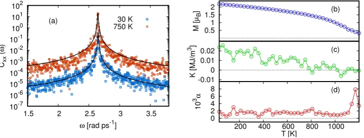
4.2 Results of a FMR simulation for bcc Fe. Panel (a) shows the FMR
spectrum at 30 K (blue symbols) and 750 K (red symbols), where the
black lines represent the curves fitted with the function in Eq. (4.31).
The figure on the right-hand-side displays the temperature dependence
of the total magnetisation (b), the macroscopic anisotropy constant
(c) and the Gilbert damping (d) as extracted from the fit results. . . 124
4.3 Dynamic structure factor for bcc Fe. The colour scale represents the
logarithm of the power spectral density (PSD). . . 125
4.4 The variation of the energy and the probability distributions for the
spin length of L10 FePt during the dynamics described by the GSE.
Left: the longitudinal (hollow symbols) and total (full symbols)
ener-gies for Fe (blue) and Pt (orange) depending on the respective spin
length. The energy scale on the left-hand side refers to Fe spins, the
one on the right-hand side to Pt spins, are pointed out by the coloured
arrows. Right: probability distribution for the Fe (b) and Pt (c) local
spins for different temperatures. . . 128
4.5 Temperature dependence of the anisotropy predicted within the
ex-tended spin model (blue squares), by using the Hamiltonian in Eq. (4.37)
without the longitudinal energy and the standard LLG equation
(or-ange circles), and by employing the GSE (green triangles). . . 129
4.6 Bias dependence of the switching time in Fe (red) and Fe/Cu (blue)
free layers at 0 K. The lines represent the result of a fit to the function
defined in Eq. (4.51) the spin dynamics data (symbols). . . 134
4.7 Current-induced switching in Fe (a) and Fe/Cu (b) free layers at 0 K
for an applied field of 1 T and different voltages. . . 136
4.8 Bias dependence of the switching times in (a) Fe and (b) Fe/Cu at 0 K
(black), 100 K (red), 200 K (blue), 300 K (green) and 400 K (purple).
The dashed lines show the trend of the average switching time for a
4.9 Study of time-dependent spin correlations during the magnetisation
switching at 0 K for Fe (red) and Fe/Cu (blue) free layers. Left panel:
(a) thexxand (b) thezz component and (c) the total auto-correlation
function for the spin at the MgO/free layer interface. Right panel: (d)
thexxand (e) thezzcomponent and (f) the total correlation function
between the interfacial spin and all the others. . . 138
4.10 Study of the bias dependence of the spin correlations for the switching
dynamics in (left panel) Fe and (right panel) Fe/Cu free layers. The
top (bottom) panels show the total auto- (spin-spin) correlation
func-tions for each free layer for voltages of (red lines) 1.1, (green lines) 1.5
and (blue lines) 2.0 in units of the critical voltage. . . 139
4.11 Study of the temperature dependence of the spin correlations for the
switching dynamics in (left) Fe and (right) Fe/Cu free layers. The top
(bottom) panels show the total auto- (spin-spin) correlation functions
for each free layer for a voltage of V = 1.1Vc at (red lines) 100 K,
(green lines) 200 K, (blue lines) 300 K and (purple lines) 400 K. . . . 140
4.12 Left panel: Graphical representation of the system setup for spin
dy-namics simulations with disordered barrier. The inner core is here
composed by MTJs with a 5 MgO MLs, while 6 MLs are considered
for the outer core. Right panel: trajectories of the magnetisation
switching at 10 K (purple) and 300 K (green) for disk radii, R, of (b)
32 and (c) 16 unit cells. Courtesy of Dr. Matthew Ellis. . . 141
4.13 Snapshot of the switching dynamics in a disordered Fe/MgO/Fe
nano-pillar for a constant current of 50 GAm−1. The figures on the left-hand
side represent the z component of the atomic spins throughout the
disc, where right-hand side panels show the distribution of the current
density. Here the linear size of the disorder feature is 2 for the top
4.14 Bias dependence of the switching time in FePt (red) and FePt/Fe
(blue) free layers at 0 K. A field of 5.5 T was applied in the case of
FePt/Fe, while no external field was applied for the FePt layer. The
lines represent the result of a fit of the function defined in Eq. (4.51).
The corresponding data are the symbols. . . 144
4.15 Current-induced switching in FePt (a) and FePt/Fe (b) free layers at
0 K A field of 5.5 T is applied in the case of FePt/Fe, while no external
field was applied for the FePt layer. . . 146
4.16 Bias dependence of the switching times in (a) FePt and (b) FePt/Fe
at 0 K (black symbols), 100 K (red), 200 K (blue), 300 K (green) and
400 K (purple). For data sets obtained at finite temperatures the lines
show the trend of the average switching time for a given voltage. A
field of 5.5 T is applied in the case of FePt/Fe, while no external field
was applied for the FePt layer. . . 147
4.17 Study of time-dependent spin correlations during magnetisation
switch-ing at 0 K FePt (red) and FePt/Fe (blue) free layers. Left panel: (a)
the xx and (b) the zz component and (c) the total auto-correlation
function for the spin at the MgO/free layer interface. Right panel:
(d) the xx and (e) the zz component and (f) the total correlation
function between the interfacial spin and all the others. The colors
indicate the distance of each spin from the interfacial one (i = 0),
where blue denotes the closest site and red denotes the most far away. 148
4.18 Study of the (left) bias and (right) temperature dependence of the
spin correlations in a Fe/MgO/FePt junction. The top panels show
the auto-correlation functions, while the bottom panels display
spin-spin correlations. For the latter case full lines correspond to the closest
spin (i = 1) to the interfacial one, while dashed lines are relative to
the one furthest away from the interface. Left: the different colors
5.1 Left panel: unit cell for Mn3Ga. Small spheres represent the Ga atoms,
large spheres the Mn atoms. In particular, the red arrows indicate the
2b sites, and the blue arrows the 4a sites. Right panel: temperature
dependence of the average magnetisation for the 2b sites (green lines),
the 4a sites (blue lines) and all sites (orange lines). The full (dashed)
lines are obtained assuming uniform (different) anisotropy at
non-equivalent sites. . . 153
5.2 FMR spectrum for Mn3Ga at different temperatures with (a) uniform
and (b) different anisotropy for non-equivalent sites. We find two
different resonant modes, one at lower frequency (∼20 THz) and a
second, weaker, one at a higher frequency. . . 154
5.3 Left panel: low frequency FMR spectrum for Mn3Ga at different
tem-peratures with uniform anisotropy constant at all sites. The black lines
show the result of the best fit according to Eq. (4.31) of the resonant
peak. Right panel: (b) the total magnetisation, (c) the macroscopic
anisotropy constant and (d) the Gilbert damping extracted from the
fitting of the low frequency resonant peak for different temperatures. 156
5.4 Dynamic structure factor for Mn3Ga at 10 K with (a) uniform and (b)
different anisotropy for nonequivalent sites. . . 157
5.5 Magnetic unit cell of Fe2MnGa. The arrows show the atomic magnetic
moments in the (a) ferromagnetic (FM) and (b) anti-ferromagnetic
configuration. The different colors of the spheres defines the atomic
species: red for Fe, violet for Mn and gray for Ga. . . 158
5.6 Calculated inter-atomic exchange parameters for Mn-Mn (purple),
Mn-Fe (blue) and Fe-Fe (red) sites depending on the inter-site
dis-tance expressed in units of the in-plane lattice constant,a. Data points
represented by circles are obtained with aligned Mn moments, while
the ones denoted with squares are obtained with antiferromagnetically
5.7 Left panel: temperature dependence of the average spin for each
sublattice in AF Fe2MnGa. Right panel: magnon spectrum for AF
Fe2MnGa. . . 161
5.8 Results of ferromagnetic resonance simulations in antiferromagnetic
Fe2MnGa. Left: FMR spectrum for the AF configuration of Fe2MnGa
at different temperatures. The black lines show the result of our best
fit of the resonant peak. Right: temperature dependence of [panel
(b)] the total magnetisation, [panel (c)] the macroscopic anisotropy
constant and [panel (c)] the Gilbert damping extracted from the fitting
of the resonant peak. . . 163
5.9 Representation of a Fe/MgO/Fe2MnGa junction. The different color
of the spheres corresponds to different atomic species: red for Fe, blue
for Mg, green for O, violet for Mn and gray for Ga. The dashed lines
identify the two nonequivalent planes in Fe2MnGa along the transport
direction. The plane denoted as Mn1 contains the closest Mn to the
MgO interface, while in the plane Mn2 the first site after the interfacial
Fe atoms is occupied by Ga. . . 164
5.10 Atomic magnetic moments in the free layer of a Fe/MgO/Fe2MnGa
junction with aligned (blue circles) and anti-aligned (black squares)
Mn atoms. The colored background defines the atomic species: red
for Fe, violet for Mn, gray for Ga, blue for O and green for Mg. . . . 165
5.11 Energy dependent transmission coefficients for majority- (full lines)
and minority-spin (dashed lines) for the FM (red lines) and AFM
5.12 Study of the torkance in Fe2MnGa free layers with AFM (left) and
FM (right) magnetic ordering. In all panels the colored background
indicates the atomic species: blue for O, green for Mg, red for Fe, gray
for Ga, pink for Mn. The top panels display the relevant components
of the exchange and correlation field, ∆, the middle panels the
non-equilibrium spin density, dm/dV, and the bottom panels the torkance
per unit ofµB/eand area, τ. . . 166
5.13 Calculated torkance per unit ofµB/eand ares in Fe2MnGa free layers
with AFM (left) and FM (right) magnetic ordering. In all panels the
colored background indicates the atomic species: blue for O, green for
Mg, red for Fe, gray for Ga, pink for Mn. Top panels and bottom
panels show the torkance acting on the plane Mn1 (top panels) and
the plane Mn2 (bottom panels) as function of the distance from the
Magnetic random access memories
“The story so far: in the beginning the Universe was created. This has made many people very angry and has been widely
regarded as a bad move.”
- Douglas Adams
The continuous miniaturisation and performance enhancement of electronic
com-ponents have been essential to improve the quality of our everyday life. The advent of
portable electronic devices led to a growing inclusion of technology in daily tasks and
consequently to an increasing demand of efficient tools for data processing and
stor-age. Modern computers largely rely on dynamic random-access memory (DRAM)
technologies for computing power. These devices store data in the charge state of a
capacitor made of two metallic plates separated by a dielectric (mostly Si). Although
information can be efficiently written by simply modifying the amount of charge
ac-cumulated in the capacitor, the reading procedure is more energetically expensive,
since it requires deleting and rewriting the charge state. In addition, charge leakage
implies the need of a frequent charge refresh to prevent the loss of information, and
such effect grows as the capacitor size is reduced. The destructive read protocol, the
issue of charge refresh and the need of a constant power supply to maintain the stored
data imply elevated power consumption and poor scalability. Therefore, these
will be required for future technological developments. Improvements of DRAMs
are still considered to be possible thanks to the introduction of three-dimensional
structures and materials with high relative dielectric constant [1], but their intrinsic
limitations encourage the search of alternative technologies.
The idea of replacing DRAMs with memories that do not require constant power
to retain data, i.e. that are non-volatile, is particularly attractive due to the low
energy operational costs. Among the memories currently available to the public,
flash memory is the only one which is non-volatile and at the same time has
ad-equate read/write speed to replace DRAMs. Flash memories store information in
the charge state of a transistor that is electrically isolated to preserve the
non-volatility. Nevertheless, the device integrity deteriorates after a relatively low
num-ber of program-erase cycles. Together with their high fabrication costs, the reduced
durability of flash memories makes them unsuitable to be used as main processing
units. In order to bypass the low endurance of flash memories and the scalability
and volatility issues of DRAMs, various memory prototypes that do not use charge
states to store information were proposed. Ferroelectric memories (FeRAMs) [2]
have a structure, which is similar to DRAMs, but they replace the dielectric layer
with a ferroelectric slab, i.e. made of a material with a spontaneous electric
polar-ization. The charged/discharged capacitor configurations that embody the “0” and
“1” states in DRAMs are here represented by the two opposite orientations of the
electric polarisation in the active layer, which can be controlled by external electric
fields. As an alternative, an analogous role can be played by the different phases of
a material, provided that the phase transformation can be efficiently and accurately
performed. State-of-the-art phase changing memories (PCMs) [3] adopt a slab of
GeSbTe as active layer. In fact, it is possible to liquefy GeSbTe through heating
to then obtain either an amorphous or crystalline phase by controlling the
rapid-ity of its cooling. Both the latter two prototypes are considered to be promising
candidates for future non-volatile memories. On the one hand, FeMRAMs have
ex-ceptional write speed, high endurance and ultra-low power consumption. However,
PCMs offer good scalability and at the same time fast data access and write/erase
speeds, but their operational temperature range is rather limited. Neither of these
devices is thus suitable for applications such as automotive vehicles that require
en-ergy efficient, high density and durable memories, that must also be able to maintain
satisfactory performances at high temperatures.
Magnetic random-access memories (MRAMs) are currently believed to be the
technology that is more likely to be able to satisfy such requirements. Such devices
store data in the direction of the magnetisation vector of a magnetic layer: if the “0”
state is represented by a specific orientation of such vector, the opposite direction will
represent the “1” state. Their working principle is routed in the use of spin polarised
electric currents to perform both the reading and the writing procedures. This
allows for extremely low energy consumption, high durability and fast operation.
Furthermore, the appropriate choice of the magnetic material yields natural
non-volatility, high scalability and elevated resistance to radiation and high temperatures.
These reasons make MRAMs also potential candidates for a “universal memory”, i.e.
capable of replacing the functions currently covered by the simultaneous employment
of DRAMs, flash and static RAMs (SRAMs).
This chapter begins with a review of the main discoveries that made the
real-isation of magnetic memories possible, together with the physical phenomena that
underpin their operating principles. An analysis of the possible material choices for
efficient MRAMs follows, including a description of the relative issues and challenges.
In conclusion, an overview of the contents of the rest of this thesis will be presented.
1.1
The development of STT-MRAMs
1.1.1
Giant magnetoresistance and the advent of spintronics
The working principles of electronic devices rely on the manipulation of electrons
through their intrinsic charge. It is then only natural to wonder whether it is
the field of spin electronics, or spintronics, magnetic materials are embedded into
electronic components to generate spin polarised electrical currents and increase the
capability and the functionality of electronic devices. The idea that the spin state
of electrons influences their mobility can be traced back to Mott’s early work on the
spin dependence of the conduction properties of ferromagnets [4]. The general spin
state of an electron is defined as a 3-component vector with modulus~/2, hence can
be represented as the linear combination of two fundamental states. It is customary
to identify these two states with the directions parallel and anti-parallel to the spin
quantisation axis, thus call them as the spin-↑ and spin-↓ state. Since
ferromag-nets are characterised by an asymmetry in the population of the two spin states,
the latter are also known as majority- and minority-spin states. In particular, Mott
proposed that electrons in spin-↑ and spin-↓ states constitute two independent
con-ducting channels. Since the electrical resistivity depends on the density of states
at the Fermi level, the spin asymmetry in the electronic population of ferromagnets
generates a difference in the resistivity of the two spin channels. Such prediction
was later observed experimentally through conduction measurements in doped Ni
[5]. These findings already suggest that the magnetic state of a material plays a role
in its electrical resistance, although such effect is not pronounced for the scale and
systems considered in Refs. [4, 5].
The advent of deposition techniques, such as molecular beam epitaxy (MBE),
in the 1980s made it possible the fabrication of thin films down to the nm scale.
This proved to be vital for the discovery of new magnetoresistance phenomena that
appear where the layer thicknesses are comparable to the mean free path of
elec-trons. In the early years of research on magnetic thin films, multilayers composed of
alternating Fe and Cr layers emerged as the ideal system where the relative
orienta-tion of magnetisaorienta-tions of adjacent layers could be controlled. Although the presence
of antiferromagnetic layer-exchange couplings favours the anti-parallel alignment of
the magnetisations [6], the parallel alignment can be realised by applying external
magnetic fields. The electrical resistance offered by the system when adjacent
alignment. The difference in the two resistances is essentially due to the change
in available states throughout the stack for each spin channel, as represented in
Fig. 1.1. If the magnetisations are all parallel, the majority spin state will have
the same direction, say ↑, for all magnetic layers. As a consequence, the constantly
higher number of states close to the Fermi energy available by spin-↑ electrons
im-plies that the resistivity for the spin-↑ channel will be significantly lower than the
one for the spin-↓ channel. On the contrary, in the anti-parallel configuration the
majority spin state alternates direction between adjacent magnetic layers, and so
does the number of available states for each spin channel. The conductivity of spin-↑
and spin-↓ electrons is thus equally suppressed in the antiparallel state. This
ef-fect is commonly known as giant magnetoresistance (GMR) and was simultaneously
discovered by Albert Fert and Peter Gr¨unberg [7, 8], reason for which they were
[image:30.595.125.501.387.518.2]jointly awarded the Nobel price for physics in 2007. Early studies on GMR were
Figure 1.1: (a) Graphic representation of the density of states of a ferromagnet
around the Fermi energy. (b) Schematic illustration of the GMR effect. The green
arrows represent the orientation of the magnetisation vectors, while red (blue) arrows
represent the intensity of the transmission for the majority (minority) spin channel.
For parallel magnetisations (left) the conductivity is enhanced for one spin channel
and suppressed for the other, so that the short-circuit through the former channel
implies a reduced resistance. On the contrary, in the anti-parallel state (right) the two
spin channels have the same conductivity, hence the resistance is higher compared
all performed with current flowing along the layers direction, i.e. with the geometry
that is nowadays known as “current in plane” (CIP). However, geometries where the
current is driven parallel to the stacking direction, i.e. in the “current perpendicular
to plane” (CPP) geometry, were found more convenient for applications [9,10]. First
of all, the difference between the resistances in the parallel (P), RP, and antiparallel
(AP) configurations, usually quantified through theGMR ratio,
GM R = RAP−RP
RP
, (1.1)
is more pronounced in the CPP geometry with respect to the CIP one [9].
Accord-ing to theoretical investigations [11], this is due to the reduced spin-asymmetry of
interfacial scattering in the CIP geometry.
GMR devices represent one of the first prototypes of magnetic memories.
How-ever, magnetisation switching in metallic spin valves is not efficient enough to offer
a competitive alternative. Nevertheless, the GMR effect is widely used to this day
to construct efficient magnetic field sensors.
1.1.2
Magnetic tunnelling junctions
The separation of two magnetic layers with an insulating barrier, i. e. employing a
magnetic tunnelling junction (MTJ), offers an alternative to metallic junctions since
the spacer strongly suppresses interlayer couplings. MTJs were found to have
magne-toresistive properties as early as 1975 by Julli´ere [12]. In fact, thin enough insulating
barriers allow the flow of electric currents between the two ferromagnetic electrodes
thanks to the establishment of a tunnelling regime. These experiments proved that
magnetic tunnelling junctions exhibit an effect similar to the giant
magnetoresis-tance, nowadays known as tunnelling magnetoresistance (TMR). The TMR effect
was explained by Julli´ere neglecting spin-flip phenomena and using a two current
model analogous to the one adopted above for explaining the GMR [Fig. 1.1 (b)].
The argument is based on estimating the conductance in terms of the transmission
spin electrons will have tunnelling probabilities 1−t1 and 1−t2, respectively. Hence, the total conductance,GP, GAP, in the two possible magnetic configuration are given by
GP=t1t2+ (1−t1)(1−t2) =
1 +P1P2
2 , (1.2)
GAP =t1(1−t2) + (1−t1)t2 =
1− P1P2
2 , (1.3)
wherePi = 2ti−1 denotes the spin polarisation of thei-th ferromagnet, withi= 1,2.
Since by definition 0≤ Pi ≤1, we find that the conductance is higher in the P
con-figuration than in the AP one, as in the case of GMR. Moreover, Eqs. (1.2) and (1.3)
can be easily combined to yield an expression for the tunnelling magnetoresistance
ratio in terms of the spin polarisations, i.e.
T M R≡ GP−GAP
GAP
= 2P1P2 1− P1P2
. (1.4)
This equation is known as the Julli´ere formula for the TMR ratio and its validity is
limited to cases, where spin-flip processes are negligible. Since spin excitations imply
a breakdown of the independence of the two spin channels, conditions that favour
their presence (high voltages, elevated temperatures or concentration of defects) will
unavoidably cause a deterioration of the TMR. Nevertheless, Eq. (1.4) shows that
the TMR is maximised for P1 = P2 = 1, thus implying that a high degree of spin polarisation of the current is essential to obtain high TMRs.
In his experiments Julli´ere employed Fe/GeO/Co junctions with barrier
thick-nesses ranging between 10 and 15 nm, measuring TMR ratios of about 14% at low
temperatures. The modest magnitude of such effect was due to the relatively low
spin polarisation of the magnetic electrodes, the large spacer thickness and the
amor-phous barrier. Hence, the discovery of the TMR effect did not attract much attention
at the time. The interest in MTJs was renewed with the development of GMR, and
in the mid 1990s room temperature (RT) TMRs of 11.8% and 18% were observed in
FeCo/Al2O3/Co and Fe/Al2O3/Fe MTJs by Moodera [14] and Miyazaki [15], respec-tively. The tunnelling barriers in these cases had thicknesses below 5 nm and were
strongly enhance the TMR ratio, if it is well matched with the electronic structure
of the ferromagnets. In fact, tunnelling properties across crystalline insulators were
shown to be remarkably influenced by the spatial symmetry of the Bloch states,
meaning that the barrier favours the tunnelling of electrons in states with certain
symmetries (Fig. 1.2). As a consequence, if the occupation of the electronic states
which tunnelling is more favourable is higher for one spin state than for the other,
the transmission probabilities for the two spin channels will be remarkably different.
In other terms, the insulator can effectively select electrons depending on their spin
state, i.e. acting as a spin filter.
The first prediction of the so-called spin filtering effect is due to Butler et al.
[17] and Mathlon et al. [18] who calculated the electronic, magnetic and transport
properties of Fe(100)/MgO(100)/Fe(100) tunnelling junctions. The authors show
that in such structures the conductance is dominated by electrons with wave-vectors
orthogonal to the current direction, and that Bloch states with a particular
symme-try have particularly low decay rate across MgO. The latter feature can be evinced
Figure 1.2: Schematic of the difference tunnelling properties in crystalline MgO
and amorphous Al2O3 barriers. In Fe/MgO/Fe tunnelling is enhanced for electrons
of a ∆1 symmetry state, while Bloch state symmetries do not play a role in the determination of tunnelling probabilities across amorphous barriers. Image credit:
by comparing the (real) band structure of Fe with the complex band structure of
MgO [panels (a) to (d) of Fig. 1.3]. Although in infinite solid state systems the
Schr¨odinger equation admits solutions only for real momentum vectors, k, solutions
corresponding to purely imaginary vectors, κ, appear in the presence of interfaces.
Their physical meaning relates to vanishing states propagating from the interface
within the material. In particular, states with elevated imaginary wavenumber,
iden-tified with κ2 = |κ|2, will have a lower probability of tunnelling across the barrier, henceκ2 quantifies the decay factor in the insulator. Panel (a) of Fig.1.3 highlights the difference in symmetry states of different segments of the first Brillouin Zone
in the calculated real band structure of MgO, while panel (b) displays the
associ-ated complex bands. For simplicity, we assume here that the transport direction
is aligned with the z axis. Given that electrons propagating orthogonally to the
stacking direction constitute most of the current, only the corresponding direction
in k-space is displayed. By convention, ∆1 states transform like linear combinations of functions with 1, z and 2z2−x2−y2 symmetry; ∆5 denotes symmetry properties of linear combinations of functions with zxand zy symmetry, ∆20 of functions with
Figure 1.3: Comparison between the real (a) and complex (b) band structure of
MgO and the majority (c) and minority (d) spin real band structure of bcc Fe.
y2 −z2 symmetry. From [Fig. 1.3 (b)] it is then evident that the decay rate at the Fermi level of ∆1 states is significantly smaller than that of states with ∆5 or ∆20
symmetries. Importantly, the majority spin band structure of Fe [Fig. 1.3 (c)] has
a ∆1 band crossing the Fermi level, while the same does not hold for the minority spin bands [Fig. 1.3 (d)]. In conclusion, the symmetry match between the complex
bands in MgO and the real bands in Fe allows for a strongly spin polarised current
across the barrier, hence a large TMR ratio, in Fe/MgO/Fe junctions.
The findings presented by Butler et al. were later confirmed with the observation
of room temperatures TMRs as large as 180% for single-crystal Fe/MgO/Fe [19] and
220% for polycrystalline MTJs [20]. It must be noted, however, that all measured
TMRs in Fe/MgO/Fe MTJs at both low and high temperature are systematically
lower than the theoretical estimations of several 1000%. The cause of this
disagree-ment is related to the presence of a wide range of deviations from epitaxy at the
Fe/MgO interfaces [21, 22]. For example, the formation of an interfacial FeO layer
was shown to strongly deteriorate the spin filtering properties [23]. In conclusion, the
optimisation the TMR of Fe/MgO/Fe MTJs ultimately translates into an engineering
of Fe/MgO interfaces.
The realisation of high TMRs at room temperatures made it possible to use MTJs
to store information, since the TMR can be exploited to efficiently read the
mag-netic state (P or AP). Nevertheless, writing procedures relying on the application of
magnetic fields imply a high power consumption because of the large fields required
to switch the magnetisations between the two states. Furthermore, the difficulties in
realising strictly localised magnetic fields considerably reduce the affordable
integra-tion density. Hence, an alternative writing protocol is needed for efficient memories.
1.1.3
Spin transfer torque random access memories
The possibility of inducing magnetisation dynamics through the use of spin polarised
currents was first theorised by Slonczewski [24] and Berger [25] independently. The
two authors proposed the idea that a spin polarised current injected in a magnetic
Figure 1.4: Schematic representation of the mechanism that gives rise to a
spin-transfer torque in an MTJ. If an electric current is flowing from left to right, it
enters the free (right hand side) layer with the spin polarisation of the reference
(left hand side) magnetic layer. The exchange interaction causes electrons emerging
from the barrier to adapt their spins to the static local magnetisation, MF ree, thus
transferring angular momentum to the free layer. As a result of spin conservation,
the local magnetisation vector is driven to align with the spin polarisation of the
current, i.e. it experiences an effective spin torque.
momentum to the local magnetisation. In particular, the effect is such that the static
magnetisation vector is driven towards the alignment with the spin polarisation of
the current. In other terms, a spin polarised current effectively exerts aspin transfer
torque (STT) on the static magnetisation vector and can be exploited to control its
orientation.
In order to elucidate this mechanism we consider a magnetic tunnelling junction
where the magnetisations of the two magnetic layers are misaligned, as shown in
Fig. 1.4. In these conditions a current flowing from the left-hand side to the
right-hand side enters the barrier with a spin polarisation, which is aligned with the
magnetisation of the former. For the moment, the spacer is assumed to yield a
perfectly spin-polarised current. However, a similar argument holds for cases such
as metallic spacers where the polarisation of the injected current is not 100%. The
spins aligned with the magnetisation of the left layer,MRef. Given the magnetisation misalignment, the spin quantisation axis of the transport electrons is not the same
of the one of the free layer. As a consequence, the exchange interaction between
the spins of the transport electrons and the static magnetisation, MFree, causes the former to align with the latter. In turn, the magnetisation vector of the free layer is
driven to align with the direction of the current, i. e.MRef, by spin conservation, and such effect corresponds to the spin transfer torque. Since the angular momentum
carried by the current is provided by the left-hand side layer, MRef also feels a torque because of an analogous mechanism, and by spin conservation it has the
same intensity but opposite sign than the torque acting MFree. Nevertheless, the multilayered structure can be engineered so that reference layer can act as reservoir
for angular momentum. Hence, its magnetisation vector can be kept constant and
exploited as reference, while the free layer can be driven to align or antialign with
the former by applying the current in a verse or the other.
The exploitation of the TMR and STT effects thus allow to effectively read and
write the magnetic state of an MTJ by the means of an electric current, and
em-bodies the operational principle of spin-transfer torques random-access memories
(STT-MRAMs). Such prototypes represent a significant improvement with respect
to field-switched MRAMs for their potentially lower energy consumption and
en-hanced scalability, since STT-MRAM cells can reach sub-20 nm size compared to the
60 nm×150 nm limit for field-switched MRAMs. The realisation of high performance
memories depends, however, on a thorough engineering of the stack containing the
magnetic tunnelling junction. The goal of the structure design is to obtain devices
with high TMR at room temperature, where magnetisation reversal can be realised
with the lowest current intensity possible and remains stable to thermal fluctuations.
The accomplishment of such objective requires, however, an understanding of which
properties influence the magnetisation switching.
The dynamics of the global magnetisation vector, M, in the presence of spin
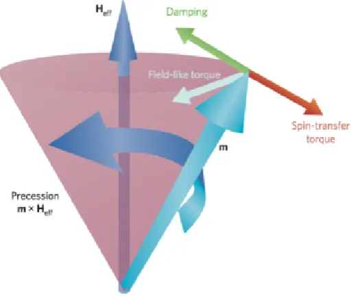
Figure 1.5: Schematic representation of current-driven magnetisation dynamics. The
field-like torque and the interaction with the effective field,Heff, induce a precession aroundHeff, while the spin-transfer torque and damping effects control the alignment between the magnetisation vector, m, and Heff. Image credit: [26].
(LLGS),
∂M
∂t =−γM ×Heff−αM ×
∂M
∂t +T. (1.5)
Here we will limit the discussion of this equation to a qualitative description of the
defining features of spin dynamics in STT-MRAMs, while a more detailed analysis
will be presented in § 4. The first term of Eq. (1.5) describes the precession motion
of the magnetisation,M, around the effective field acting onM,
Heff=−
1
|M| ∂E
∂M =−
1
|M| ∂ ∂M
Eexch+Eapp+Eani
(1.6)
with γ denoting the gyromagnetic ratio for the electron. The last term of Eq. (1.6)
describes the contributions of the total magnetic energy that are relevant for the
the so-called easy axis and is determined by various factors, ranging from the
geo-metrical shape of single crystal magnets to the presence of interfaces and spin-orbit
mediated interactions between atomic spins and the crystal structure
(magnetocrys-talline anisotropy). The second term in Eq. (1.5) is a “friction” term that drives the
tendency of the magnetisation to align along its equilibrium orientation, i. e. the
easy axis. The strength of this torque is quantified by the phenomenological damping
parameter, α, known as Gilbert damping. Such quantity is fundamental to
deter-mine the magnetisation switching times since it embodies the friction-like effect to
be overcome by the spin torque in order to achieve the magnetisation reversal. Let
us note that the current-induced torques are introduced as a vectorial quantity, T,
which is traditionally divided into two components, one contributing to the reversal
motion, one to the precession [Fig. 1.5]. The former corresponds to the spin-transfer
torque described above, and is also known as in-plane torque since it does not drive
the magnetisation vector out of the plane defined by the magnetisations of the two
magnetic layers. In contrast, the out-of-plane or field-like torque is parallel to the
precession term of Eq. (1.5) and it is normally attributed to phenomena such as the
precession of electronic spins or the presence of transport electrons with minority
spin state. Although the field-like torque does not influence directly the
magnetisa-tion reversal, it was argued that its interplay with the in-plane component plays a
role in the stability of the switching process [27, 26]. Nevertheless, the out-of-plane
component can be exploited to force the magnetisation into a constant precession
with frequencies in the microwave range, hence to realise spin torque nano-oscillators
(STNOs) [28].
1.2
Designing magnetic tunnel junctions for
high-performance memories
In the last section we showed that the use of MTJs in memory applications
spin-transfer torque writing can potentially allow for extremely low energy consumption
and switching times of the order of the ns. The realisation of such potential into
efficient STT-MRAMs requires, however, the minimisation of bit sizes and of the
current intensities, while maintaining high performances at elevated temperatures.
This translates in the search for multilayered structures with reduced cross sections,
with high TMRs at room temperature (>150%) for efficient reading and that can be
written with low current intensity. The exceptional spin filtering performed by MgO
barriers matched with bcc Fe layers has made Fe/MgO/Fe the most chosen starting
material composition for the fabrication of high TMR MTJs. Nevertheless, the high
Gilbert damping of Fe makes junctions with perpendicular geometry and efficient
switching troublesome to realise. In addition, the spin polarisation induced by a
pure Fe layer suffers of the presence of parasitic tunnelling of ∆2 and ∆5 symmetry electrons, pushing the search for material alternatives. Contrarily to Fe, in bcc Co
only ∆1 states populate the majority band at the Fermi level hence the higher spin polarisation grants Co/MgO/Co junctions a higher predicted TMR than Fe-based
MTJs [29]. Furthermore, the higher magnetic anisotropy of Co implies enhanced
stability of the magnetic properties to thermal fluctuations. Nevertheless, when Co
is deposited on MgO it nucleates in a non uniform island-like pattern rather than
growing in a regular bcc lattice. Such deviation from an ideal crystalline structure
strongly reduces the achievable spin polarisation, since it favours the formation of
in-terfacial resonant states that in turn enhance the tunnelling of spin-down electrons.
The use of CoxFe1–x alloys offers improved spin polarisation and crystalline order compared to elemental crystals. Although the optimal Co concentration is debated,
rich Co compositions are normally preferred for higher stability to temperature
fluc-tuations. The resulting TMR then depends on the amount of defects and disorder at
the magnet/insulator interfaces, since any additional source of scattering alters the
predicted electronic states and hence yields deviations from ideal spin filtering. The
key objective to be achieved in order to realise high TMR MTJs is thus to engineer
multilayered structures that can be grown while keeping the ferromagnet/insulator
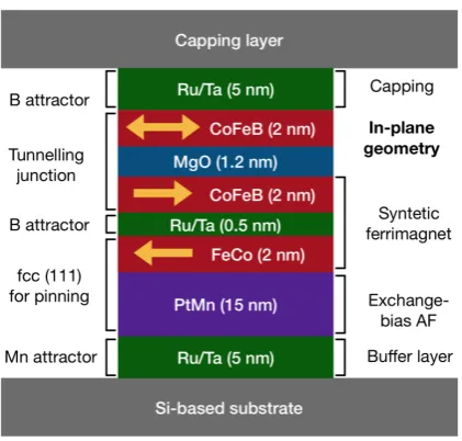
Figure 1.6: Typical multilayered stack including a magnetic tunnel junction with an
in-plane magnetisation geometry for STT-MRAM applications.
in an amorphous phase, and crystallisation and epitaxy are then obtained through
annealing. This is possible thanks to the high stability of the MgO rock salt-like
structure, which dictates the crystal phase of the stack during the high temperature
annealing [30]. Moreover, the addition of B to CoxFe1–x was found to help the crys-tallisation of the electrodes on MgO and TMRs beyond 200% at room temperature
were observed in (CoFe)80B20/MgO/(CoFe)80B20 MTJs [31].
Nevertheless, the capability of fabricating high TMR junctions alone is not
suf-ficient to realise efsuf-ficient STT-MRAMs. The key challenge is in fact to achieve low
write currents and good data retention at the same time, meaning that the free
layer magnetisation is required to be stable to thermal noise but reversible with low
current intensities. Moreover, the reliability of the reading and writing procedures
heavily depends on how effectively the magnetisation of the reference layer can be
constrained. In early prototypes of STT-MRAMs magnetisation pinning was
re-alised exploiting the exchange bias coupling exhorted by an antiferromagnetic layer
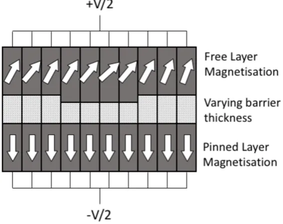
to form a synthetic ferrimagnet (SyF). Fig. 1.6 shows the typical multilayered
struc-ture adopted with such a purpose. Starting from the bottom of the stack, a thick (∼
in a fcc structure oriented along the (111) on top of a seed layer usually made of
Ru or Ta. The 3-fold in-plane symmetry of fcc (111) lattices is commonly adopted
because of its consolidated reliability for pinning structures and growth techniques
for Si-based substrates. A relatively thin layer of the fcc CoFe is deposited on the
AF, so that the interlayer exchange coupling strongly bounds the magnetisation of
the former in a given direction. In particular, the whole structure aims to force the
magnetisations to lie in the plane defined by the films, i.e. adopting an in-plane
geometry for the magnetisations. In fact, the thickness of the ferromagnetic layers is
kept to a minimum and the pillar is edged in an elliptical pattern so that shape
con-tributions to the magnetic anisotropy aid the pinning of the magnetisations within
the plane along a single axis. As explained above, MgO offers efficient spin filtering
to currents where majority-spin electrons have the ∆1 state symmetry. The use of a ferromagnet in a crystal phase with symmetry properties analogous to MgO, i. e. with
a 4-fold in-plane symmetry, is thus essential to achieve high spin polarisations. A
metallic layer of Ru or Ta is normally interposed between the fcc FeCo layer and the
FeCoB/MgO/FeCoB junction. In this way the post-annealing crystalline structure
of the MTJ is dictated by the MgO rather than by the substrate. Furthermore, the
thickness of the metallic layer is usually kept below 1 nm so that the inter-layer
ex-change between the fcc FeCo and the bcc FeCoB layers yields an antiferromagnetic
coupling. The choice of Ru or Ta for the metallic layers is also made because they
attract B and Mn atoms during annealing [30]. This helps to prevent such atoms to
diffuse towards the interfaces with the ferromagnets and hence deteriorate the device
performances.
Although the in-plane magnetisation geometry offers a good thermal stability for
reading, it is not advantageous for energy efficient switching. In fact, the intrinsic
anisotropy field induced by the shape of the free layer adds to the anisotropy
contri-butions external to such layer, hence enhancing the energy barrier to be overcome
formula for the critical current intensity,
Ick = 2αeMSV
~P µ0
Hanik +MS 2
, (1.7)
which can be evinced from the LLGS equation (see Ref. [32] for more details). Heree
indicates the electronic charge, whileµ0 is the vacuum permeability. This expression clearly shows that the critical current depends linearly on the Gilbert damping,
α, on the saturation magnetisation of the free layer, MS, and on its volume, V,
while it is inversely proportional to the spin polarisation of the current, P. The
terms in brackets embody the effective magnetic field, where Hanik is the anisotropy contribution, while the second represents the demagnetising field. Importantly, the
two contributions have the same sign, meaning that the out-of-plane precession that
the magnetisation undergoes to while switching is obstructed by the magnetising
field, hence yielding a penalty toIc. This, however, does not occur when the easy axis
of the free layer is aligned along the stacking direction, namely it is in a
perpendicular-to-plane geometry. In this condition the critical current becomes
Ic⊥= 2αeMSV
~P
µ0 Hani⊥ −MS
, (1.8)
where the anisotropy field is here denoted as Hani⊥ to highlight its different intensity as compared to the one characteristic of in-plane geometries, Hanik . Importantly, the demagnetising field contribution has opposite sign with respect to Eq. (1.7), meaning
that the demagnetising field in this case favours the out-of-plane precession and hence
lowers the critical current.
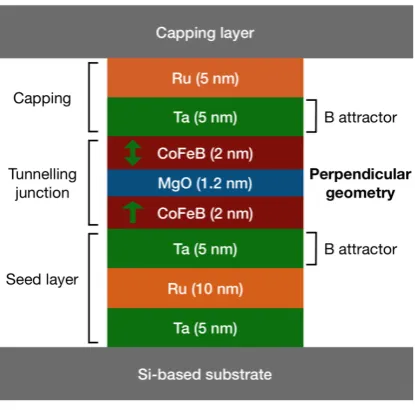
These considerations brought to the realisation of MRAMs based on junctions
with a perpendicular-to-plane magnetisation geometry (pMTJs) [33]. In contrast
to in-plane geometry devices, pinning is not obtained through inter-layer exchange
bias but the perpendicular magnetic anisotropy (PMA) arising at the CoFeB/MgO
interfaces is exploited instead. It was in fact shown that the overlap between O-pz
and hybridised transition metal dz2 orbitals at the magnetic metal/oxide interfaces
enhances the spin-orbit coupling induced splitting around the Fermi energy, thus
Figure 1.7: Typical multilayered stack including a magnetic tunnel junction with a
perpendicular-to-plane magnetisation geometry for STT-MRAM applications.
anisotropy is no longer needed, hence a circular shape of the nano-pillar
contain-ing the junction becomes more convenient than the elliptical one adopted for the
in-plane geometry. Moreover, the pinning layers can be eliminated from the
multi-layered structure that is thus significantly simplified [Fig.1.7]. The magnetic tunnel
junction is here deposited directly to a Ta/Ru/Ta buffer layer that promotes the
transition to thebcc structure of CoFeB and attracts B during annealing. The
thick-nesses of the magnetic layers are then further reduced to enhance the out-of-plane
anisotropy. This also diminishes the critical switching current given its linear
depen-dence with the volume of the free layer, as shown in Eq. (1.8). Such equation also
demonstrate that a low Gilbert damping parameter helps efficient switching. The
latter is known to grow larger with the intensity of the spin-orbit interaction, which
increases with the atomic number. Hence relatively heavy atoms such as Pt or Pd