Available Online atwww.ijcsmc.com
International Journal of Computer Science and Mobile Computing
A Monthly Journal of Computer Science and Information Technology
ISSN 2320–088X
IMPACT FACTOR: 6.017IJCSMC, Vol. 7, Issue. 6, June 2018, pg.181 – 187
Design of Schmitt Trigger Circuits Using
VTCMOS for Sub-Threshold Circuits
Syed Ameer Hussain
VLSI Design and Embedded System, Visvesvaraya Technological University, PG Center, Belgavi, India
Abstract— In this paper, a low voltage Schmitt trigger has been designed using VTMOS technique and basic gates AND, OR using VTMOS technique. In Proposed design, positive and negative biasing voltages are given for the substrates of PMOS and NMOS devices for reducing the threshold voltages of devices and allowing the circuit operation in subthreshold region. The proposed design shows 0.21nW power dissipation in 90nm technology with optimum biasing voltage is 0.4V and it can be operated for supply voltage of 0.01V.The design is implemented by using Synopsys tool (version-L-2016.06-8) using custom compiler in 90nm technology
.
Keywords— CMOS, VTCMOS, DTMOS, MTMOS, hysteresis
I.INTRODUCTION
Due to the growing demand for longer battery life in mobile devices, mobile integrated circuit (IC) designers have focused on reducing the power consumption of circuits, especially for supply voltage scaling. As a result, the supply voltage is greatly reduced, and subthreshold circuits have been developed. However, lowering the supply voltage simultaneously degrades the noise immunity of the circuit. A Schmitt trigger is one such solution that can used to enhance the noise immunity of a circuit at the expense of delay and power consumption. Unlike comparator circuits, the switching threshold of the Schmitt trigger depends on the direction of input signal transition, a phenomenon known as hysteresis. In the presence of hysteresis, the threshold voltage of the Schmitt trigger is higher than that of comparators for positive transitions and lower for negative transitions. If the amplitude of the input signal variation is less than the switching threshold difference, the output of the Schmitt trigger will not respond directly to input. This makes the Schmitt trigger immune to undesired electromagnetically coupled noise.
These bistable networks are widely used to enhance the immunity of a circuit to noise and disturbances. As they make use of sine waves, therefore it is widely used for converting analog signals into digital and to reshape sloppy, or distorted rectangular pulses.
Pedroni, V, A new technique for the design of ST circuits has been presented and tested, which allows operation, with higher speed than traditional approaches. The principle was then extended to the construction of a very compact window comparator (only eight transistors), suitable for applications where neither high accuracy nor programmability of the high, low window voltages are required[4].
Pham, A simple logical threshold voltage control circuit is proposed. It can be implemented using normal conventional CMOS inverters. The proposed circuit is able to control a logical threshold voltage of a gate linearly and continuously over a range of a power supply voltage. Applications to the Schmitt trigger circuit with controllable hysteresis and a window comparator are shown to demonstrate practical usages of the proposed circuit[4].
Haroon Rashid, Designed in 0.18 m CMOS process technology, the simulation results show that the proposed Schmitt trigger circuit’s triggering voltage can be adjusted approximately 0.5 V to 1.2 V. The proposed design is suitable to be implemented in buffers, sub-threshold SRAMs, retinal focal plane sensors, wireless transponders and pulse width modulation circuits[1].
Pratchayaporn Singhanath, This paper presents a Dynamic Threshold voltage MOSFET (DTMOS) Schmitt trigger. Cross coupled inverter with body control is employed to speed up the switching process, and control the intensity of the feedback. The proposed Schmitt trigger has been designed using 0.18 µm 0.4 V CMOS technology and analyzed using PSPICE with BSIM3V3 device models. The simulation results show rail-to-rail operation and independently adjustable switching voltages for both low-to-high (VT(LH)) and high-to-low (VT(HL)) as high as 12.5 % of the supply voltage. The power dissipation is 0.14 μW.
Inukai.T reported that variable threshold CMOS is very effective in suppressing leakage current for series connected transistors due to the increased body effect [7].
Kuroda etal proposed a variable threshold CMOS technique, which employs all low threshold devices. However, the threshold voltage is controlled using the substrate bias of the devices in a triple well CMOS process. During the active mode, the threshold voltage is decreased and during the off mode, the threshold voltage is raised. The problem with the approach is that the threshold voltage varies as the square root of body source voltage .Therefore the body-source has to considerably increase to change the threshold voltage to a reasonably higher value[8].
Narendra.S proposed a new design using forward body biasing to achieve better current drive with less short channel effects. High threshold voltage transistor with reduced leakage current is used in standby mode, and low threshold voltage transistor is employed to achieve high performance in active mode. Both high channel doping and forward body bias reduce short channel effect relaxing the scalability limit of channel length due to threshold voltage roll off and drain induced barrier lowering. This results in higher on current compared to low threshold voltage design for same off current case, improving performance. Reverse body bias can also be applied in standby mode together with forward body bias to further reduce leakage current[9].
II. DESIGNANDIMPLEMENTATION
A. CMOS SCHMITT TRIGGER
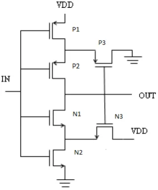
The Schmitt trigger consists of with 3 p-channel devices and 3 n-channel devices. The input of the Schmitt trigger is tied to the gates of four stacked devices. The other 2 transistors in source follower mode as shown in Fig1.
When the input is at 0V, transistors P1 and P2 are ON, and N1, N2 and P3 are OFF. Since output is high, N3 is ON and acting as a source follower, the drain of N1, which is the source of N2, is at VCC − VTH. If the input voltage is ramped up to one threshold above ground transistor N1 begins to turn ON, N1 and N3 both being ON from a voltage divider network biasing the source of N2 at roughly half the supply. When out' drops, the source of N3 follows its gate, which is out', the influence of N3 in the voltage divider with N1 rapidly diminishes, bringing output down further yet. Meanwhile P3 has started to turn ON, its gate being brought low by the rapidly dropping out'. P3 turning ON brings the source of P2 low and turns P2 OFF. With P2 OFF, out crashes down.
Fig 2. Schematic of basic CMOS Schmitt Trigger
When the input is brought low, again an identical process occurs in the upper portion of the stack and the snapping action takes place when the lower threshold is reached. Output is fed into the inverter formed by P4 and N4.The schematic diagram of basic CMOS Schmitt Trigger is shown in Fig 2.
B. CMOS SCHMITT TRIGGER USING VTCMOS
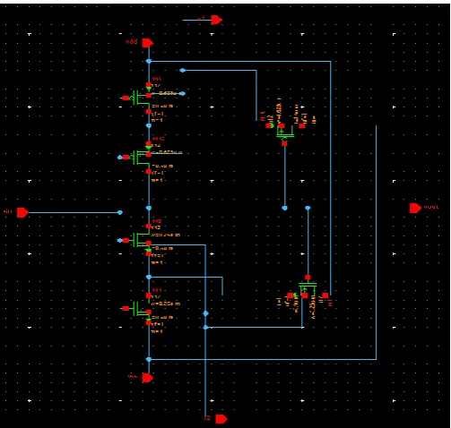
The Fig 3 shows the Schmitt trigger using VTMOS technique. This is technique one of the methods for reducing power consumption in the circuit. The main working principle is that all devices are provided with bias voltage to their substrates. For all NMOS positive bias is supplied to the substrates while in all PMOS negative bias is provided to substrate. Even though VTMOS is derived from DTMOS, it provides considerable power reduction when compared to DTMOS. As shown in Fig 3, all the substrate of 3 PMOS devices are tied together with a negative bias voltage and all the substrate of 3 NMOS devices are tied together with a positive bias voltage. Due to this the threshold voltage of the devices are reduced and the circuit can operate in sub-threshold region.
C. APPLICATION OF VTMOS USING BASIC GATES
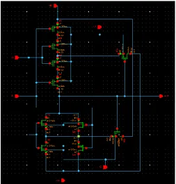
A two input Basic CMOS NAND/NOR gate can be implemented as a Schmitt trigger NAND/NOR gate by adding one PMOS and NMOS at each p-stage and N-stage of the circuit similar to M3, M6 transistors from Fig 1 in source follower mode. These transistors control the hysteresis width.
Fig 4. Schmitt Trigger NOR gate using VTCMOS
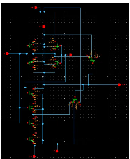
For NAND gate, when both inputs are low, all PMOS transistors turn ON and the VDD is pulled to output as high. When either of the inputs is high, VDD is pulled to Output as high through any current path formed by PMOS devices. When both inputs are low, all PMOS transistors turn OFF, all NMOS transistors turn ON and the output is low.
Fig 5. Schmitt Trigger NAND gate using VTCMOS
III. RESULTSANDDISSCUSSION
The output waveforms of Basic Schmitt trigger, VTCMOS Schmitt trigger, Schmitt trigger AND gate and Schmitt trigger NOR gate are shown in below figures respectively.
Fig 6. Output waveform of Basic Schmitt trigger
The Fig 6 shows the transient waveform of propose basic Schmitt trigger, where the input is sine signal having voltage amplitude 1v and frequency 1 kHz .The obtained output voltage is converted square wave with peak voltage 1V as shown in figure. The power dissipation is 0.54 nW and delay is 0.26 µs.
The Fig 7 shows the transient waveform of propose VTCMOS Schmitt trigger. The supply voltage is 0.5V and the power dissipation is 0.021 nW and delay is 0.46 µs.
Fig 8. Output waveform of . Schmitt Trigger NOR gate using VTCMOS
The Fig 8 and Fig 9 are output waveforms of Schmitt trigger NAND and NOR gate.
For NOR gate, the output is 1,when input A and B both are 0. The output is 0,when input A and B are either 1 or 0 or both are 1.
For NAND gate, the output is 0,when input A and B both are 1. The output is 1,when input A and B are either 1 or 0 or both are 0.
The power dissipiatin of ST AND gate is 7.442pW , It is slight higer than basic AND gate which is 7.231pW.
Fig 9. Output waveform of Schmitt Trigger NAND gate using VTCMOS TABLE I
POWER AND DELAY OF SCHMITT TRIGGERS
Parameter Basic ST VTCMOS ST
Power dissipation 0.54 nW 0.021 nW
Delay 0.26 µs 0.46 µs
TABLE II
VARIATION OF PD WITH BIASING VOLTAGE
Bias voltage(V)
Power dissipation
0 21.1pW
0.1 1.08nW
0.2 0.95nW
0.3 0.26.3nW
0.4 0.036pW
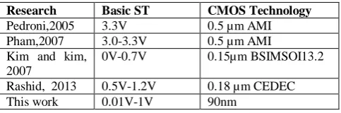
A comparison of voltage and technology used for Schmitt trigger implementation is illustrated in table 3. From the table its evident that proposed Schmitt trigger can work between 0.01V to 1.2 that lesser than the reported.
TABLE III
COMPARISON OF VOLTAGE AND TECHNOLOGY
Research Basic ST CMOS Technology
Pedroni,2005 3.3V 0.5 µm AMI
Pham,2007 3.0-3.3V 0.5 µm AMI
Kim and kim, 2007
0V-0.7V 0.15µm BSIMSOI13.2
Rashid, 2013 0.5V-1.2V 0.18 µm CEDEC
This work 0.01V-1V 90nm
IV. CONCLUSIONS
As the supply voltage of a circuit decreases, noise immunity becomes more important to guarantee signal integrity. However, by utilizing the proposed VTMOS scheme, which adjusts the threshold voltage of the MOS transistor to implement the transfer characteristics and power dissipation, is 0.021nW, while simultaneously providing improved power dissipation at the expense of a slight increase in delay 0.46 µs. The proposed design operates for voltage range of 0.01 to 1V
REFERENCES
[1] Haroon Rashid, Md. Mamun(2013)Design of a Low Voltage Schmitt Trigger in 0.18 m CMOS Process With Tunable Hysteresis,In Modern Applied Science; Vol. 7, No. 4
[2] Kim, K. K., & Kim, Y. B. (2007). Ultra-low voltage high-speed Schmitt trigger circuit in SOI MOSFET technology. IEICE ElectronicsExpress,4(19),606-611. http://dx.doi.org/10.1587/elex.4.606
[3] Pham, C. (2007). CMOS Schmitt Trigger Circuit with Controllable Hysteresis Using Logical Threshold Voltage Control Circuit. In the 6th International Conference on Computer and Information Science, 2007, pp. 48-53. Melbourne, Australia: IEEE.
[4] Chen, S. L., & Ming-Dou, K. (2005). A new Schmitttrigger circuit in a 0.13-μm 1/2.5-V CMOS process to receive 3.3-V input signals. IEEE Transactions on Circuits and Systems II: Express Briefs, 52(7), 361-365. http://dx.doi.org/10.1109/TCSII.2005.850409
[5] Pedroni, V. (2005). Low-voltage high-speed Schmitt trigger and compact window comparator. IEEE Electronics Letters, 41(22), 1213-1214. http://dx.doi.org/10.1049/el:20052799
[6] C. Zhang, A. Srivastava and P. K. Ajmera "Low voltage CMOS Schmitt trigger circuits“ Electron. Lett., vol. 39, no. 24, pp. 1696-1698, 2003
[7] S. Narendra et al., “1.1-V 1-GHz communications router with on-chip body bias in 150-nm CMOS,” in IEEE Int. Solid-State Circuits Conf. Dig. Tech. Papers, 2002, pp. 270–271.
[8] Inukai, T. Hirarnoto, T. Sakurai, "Variable threshold voltage cmos (VTCMOS) in series connected circuits", lnternational Symposium on Low Power ELectronics and Design, pp. 201-206, 2001.
[9] T. Kuroda, T. Fujita, S. Mita, T. Nagamatsu, S. Yoshioka, K. Suzuki, F. Sano, M. Norishima, M. Murota, M. Kako, M. Kinugawa, M. Kakumu, T. Sakurai, "A 0.9V 150-MHz 10-mW 4 mm2 2-D discrete cosine transform core processor with variable threshold-voltage (VT) scheme", IEEE Journal of Solid-State Circuits, vol. 31, pp. 1770-1779, 1996.