James Alan Hilder
Degree of Ph.D.
September, 2010
Intelligent Systems Group, Department of Electronics
Intrinsic variability occurs between individual MOSFET transistors caused by atomic-scale differences in the construction of devices. The impact of this variability will become a major issue in future circuit design as the devices scale below 50nm. In this thesis, the background to the causes and effects of intrinsic variability, in particular that of random dopant placement and line-edge roughness, is discuss. A system is developed which uses a genetic algorithm to attempt to optimise the dimensions of transistors within standard-cell libraries, with the aim of improving performance and reducing the impact of intrinsic variability in terms of the effect on circuit delay and power consumption. The genetic algorithm uses a multi-objective fitness function to allow a number of circuit characteristics to be considered in the evolution process. The system is tested using different standard-cell libraries from open-source and commer-cial providers, with developments and alterations to the system that have been made through-out the course of the experiments discussed. Comparisons of the performance with other optimisation techniques, hill climbing and simulated-annealing, are discussed. The optimisa-tion process concludes with the use of e-Science techniques to allow for detailed statistical analysis of the evolved designs on high-performance computing clusters. The observed results for two-input logic gates demonstrate that the technique can be effective in the reduction of statistical spread in the delay and power consumption of circuits subject to intrinsic variability. The thesis finishes with the investigation of larger circuits which are assembled from the optimised cells. A proposed design methodology is introduced, in which the processes of logic design are broken into small blocks, each of which uses techniques from evolutionary computation to improve performance. This includes an investigation into the application of a multi-objective fitness function to improve the performance of logic circuits evolved us-ing Cartesian Genetic Programmus-ing, which produces designs for logic multiplier and display driver circuits which are competitive with human-produced designs and other evolved designs. These designs are assessed for their variability tolerance, with the multiplier circuit demon-strating an improvement in delay variability.
List of Figures ix List of Tables xi Declaration xiii Hypothesis xiv Acknowledgments xv 1 Introduction 1 1.1 Background . . . 1
1.2 The Nano-CMOS Project . . . 2
1.3 Objectives . . . 3
1.4 Structure of Thesis . . . 5
2 Transistor Variability 6 2.1 Introduction . . . 6
2.2 The Metal-Oxide Semiconductor Field-Effect Transistor . . . 7
2.2.1 Structure of Field-Effect Transistors . . . 8
2.2.2 Function of Field-Effect Transistors . . . 9
2.2.3 Structure of CMOS Integrated Circuits . . . 13
2.2.4 Dielectric Materials . . . 14
2.2.5 The CMOS Fabrication Process . . . 15
2.2.6 Transistor Sizing . . . 20
2.3 Transistor Scaling . . . 23
2.3.1 Moore’s Law . . . 23
2.3.2 Technology Roadmaps . . . 25
2.3.3 Lithography Scaling . . . 27
2.4 Causes of Transistor Variability . . . 28
2.4.1 Variability due to Manufacturing Process . . . 29
2.5 Intrinsic Variability . . . 29
2.5.1 Random Dopant Placement . . . 30
2.5.2 Line-Edge Roughness . . . 32
2.5.3 Surface Roughness . . . 34
2.5.4 Poly-Silicon Grain-Edge Boundaries . . . 34
2.5.5 Temporal Variability . . . 35
2.5.6 Interconnect Variability . . . 36
2.6 Modelling Variability . . . 37
2.6.1 The SPICE Circuit Analysis Tool . . . 37
2.6.2 Simulation Techniques for modelling Variability . . . 42
2.6.3 Simulation of Intrinsic Variability in Future MOSFETS . . . 44
2.6.4 A tool for simulating variability: RandomSPICE . . . 47
2.6.5 A Variability-Aware Design Flow For VLSI Circuits . . . 49
2.7 Effect of Intrinsic Variability . . . 49
2.7.1 Impact on Threshold Voltage . . . 50
2.7.2 Impact on Yield . . . 52
2.7.3 Techniques to Limit Impact of Variability . . . 53
2.7.4 Body-Biasing and Adaptive Supplies . . . 53
2.7.5 A Special Case: Impact on SRAM . . . 54
3 Evolutionary Algorithms 57 3.1 Introduction . . . 57
3.1.1 Biological Background . . . 57
3.1.2 History of Evolutionary Computation . . . 59
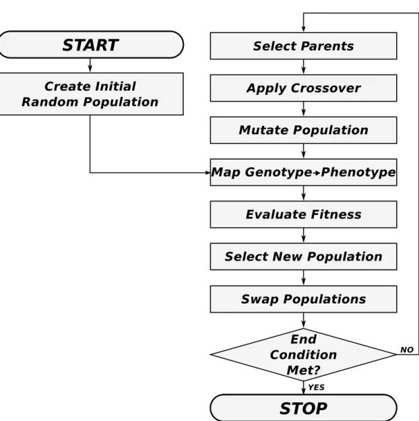
3.1.3 Operation of an Evolutionary Algorithm . . . 60
3.2 Types of Evolutionary Algorithm . . . 69
3.2.1 Genetic Algorithm . . . 69 3.2.2 Evolutionary Programming . . . 70 3.2.3 Evolutionary Strategies . . . 70 3.2.4 Genetic Programming . . . 71 3.2.5 Hybrid Methods . . . 73 3.3 Multi-Objective Selection . . . 74 3.3.1 Pareto Optimality . . . 74 ii
3.3.2 Types of Multi-Objective Evolutionary Algorithms . . . 75
3.3.3 NSGA-II . . . 77
3.4 Alternative Optimisation Algorithms . . . 78
3.4.1 Hill Climbing Algorithms . . . 78
3.4.2 Simulated Annealing . . . 79
3.5 Application of Evolution Algorithms . . . 80
3.5.1 General . . . 80
3.5.2 Uses within Electronic Circuit Design . . . 81
3.5.3 Evolution of Analogue Circuits . . . 81
3.5.4 Intrinsic Evolution . . . 87
3.5.5 Evolution of transistor models . . . 89
4 A System for Evolving Logic 91 4.1 Introduction . . . 91
4.1.1 Overview of MOTIVATED . . . 92
4.1.2 CGP-based Topology Design . . . 92
4.2 SGA for Parameter Optimisation . . . 94
4.2.1 Template Netlist . . . 95 4.2.2 Genotype . . . 100 4.2.3 Selection Process . . . 100 4.2.4 Mutation Process . . . 100 4.3 Fitness Calculation . . . 101 4.3.1 Circuit Test-Bench . . . 101 4.3.2 Fitness Objectives . . . 104 4.3.3 Multi-Objective Ranking . . . 110 4.4 Run Parameters . . . 110 4.4.1 System Parameters . . . 112 4.4.2 Evolution Parameters . . . 112 4.4.3 Circuit Parameters . . . 112
4.5 Graphical User Interface . . . 113
4.6 Use of High-Performance Computation to Accelerate MOTIVATED . . . 114
4.6.1 Background to Grid Computing . . . 114
4.6.2 The MAVENCluster . . . 114
4.6.3 The Sun Grid Engine System . . . 115
4.6.4 Alterations to code to enable cluster operation . . . 115
4.6.5 Alterations to code to enable Grid operation . . . 116 iii
4.6.6 Performance Observations . . . 117
5 Optimising Standard Cell Libraries 121 5.1 Early Results: Evolving Transistor Topologies using the SGA . . . 121
5.1.1 Methodology . . . 121
5.1.2 Results . . . 124
5.1.3 Observations . . . 124
5.2 Optimising Transistor Widths within 2-Input Combinatorial Logic Cells . . . 125
5.2.1 Two-stage Cycle for Incorporating Variability . . . 126
5.2.2 Methodology . . . 127
5.2.3 Results . . . 128
5.2.4 Observations on Results . . . 134
5.3 Comparison with Other Optimisation Algorithms . . . 137
5.3.1 Steepest-Ascent Hill Climbing . . . 137
5.3.2 SAHC With Random Walk . . . 138
5.4 Optimising Using Multiple-Voltage Sources within 2-Input Combinatorial Logic Cells . . . 139
5.4.1 Methodology . . . 139
5.4.2 Results . . . 141
5.4.3 Observations . . . 146
5.4.4 The D-Type Problem . . . 146
5.5 Optimising CGP Evolved Designs . . . 148
5.5.1 Using CGP To Evolve Standard-Cell Topologies . . . 148
5.5.2 Evolved Designs . . . 148
5.5.3 Results . . . 149
5.6 Detailed optimisation using HPC Cluster . . . 152
5.6.1 Methodology . . . 152
5.6.2 Results . . . 155
5.6.3 Observations . . . 157
6 Optimising Larger Circuits 164 6.1 Evolving Block-Level Topologies . . . 165
6.1.1 Conventional CGP To Evolve Logic Circuits . . . 166
6.1.2 Use of Multi-Objective Fitness . . . 167
6.1.3 Test Circuits . . . 168
6.1.4 Methodology . . . 169
6.1.5 Evolved Results . . . 170
6.1.6 2-Bit Multiplier . . . 171
6.1.7 3-Bit Adder . . . 173
6.1.8 3-Bit Multiplier . . . 173
6.1.9 7-Segment Display Driver . . . 177
6.1.10 Observations on Results . . . 177
6.2 Variability in Evolved Designs . . . 178
6.2.1 Methodology . . . 178
6.2.2 Results . . . 180
6.2.3 Observations . . . 183
6.3 Proposed System to Optimise Circuits at a Block Level . . . 183
6.3.1 Methodology . . . 183
6.3.2 Creation of Optimised Standard-Cell Libraries . . . 185
6.3.3 Creating of Larger Logic Topologies . . . 185
6.3.4 Optimising Larger Designs using SGA and Optimised Library . . . . 185
7 Conclusion 187 7.1 Can a genetic algorithm diminish the impact of intrinsic-variability? . . . 187
7.1.1 Is a Genetic Algorithm the best approach? . . . 190
7.2 Can a complete design process for variability tolerant circuits be created by combining evolutionary techniques? . . . 191
7.3 The Original Objectives of the nano-CMOS Project . . . 192
7.3.1 How can evolutionary techniques be used to limit the effects of pa-rameter variations? . . . 192
7.3.2 How can evolutionary techniques be used within device models to al-leviate parameter fluctuation problems? . . . 193
7.3.3 How can parameter variation datasets be best used by evolutionary techniques to improve system performance? . . . 194
7.4 Future Work . . . 194
A Additional Results 197 A.1 Creation of Schematics . . . 197
A.2 Results Tables . . . 198
A.2.1 Results . . . 198
B Pseudocode 204 B.1 Mutation Operator . . . 204 B.2 NSGA-II Implementation . . . 205
C Netlists 207
C.1 Template Netlists . . . 207 C.1.1 Template Netlist used in Early Experiments . . . 207 C.1.2 Template Netlists used in VSCLIB Optimisation . . . 208 C.1.3 Template Netlists used in multiple-voltage source experiments . . . . 210 C.1.4 Template Netlists for CGP evolved topologies . . . 212
D Glossary and List of Abbreviations 214
Bibliography 233
2.1 MOSFET Circuit Symbols . . . 8
2.2 Structure of a MOS Field-Effect Transistor . . . 8
2.3 Parasitic Capacitances in an NMOS Transistor . . . 12
2.4 Fabrication steps of an n-Well CMOS Circuit . . . 21
2.5 Fabrication steps of an n-Well CMOS Circuit . . . 22
2.6 Transistor counts in various Microprocessors and GPUs . . . 25
2.7 Clock-speeds of Intel Microprocessors . . . 26
2.8 Intrinsic Variability in a Simulated Transistor . . . 30
2.9 Atomic structures of 22nm and 4nm Transistors with RDD . . . 31
2.10 Line-Edge Roughness Patterns in Negative Photoresist . . . 33
2.11 Poly-silicon Grain Boundaries . . . 34
2.12 Small-Signal Model for a MOS Transistor . . . 38
2.13 Hierarchical Simulation Methodology for Variability . . . 50
2.14 Threshold Voltage Fluctuations due to Intrinsic Variability . . . 51
2.15 6-T SRAM Schematic and Block Diagram . . . 56
3.1 Block diagram of an evolution algorithm . . . 61
3.2 Cauchy and Gaussian Distributions . . . 66
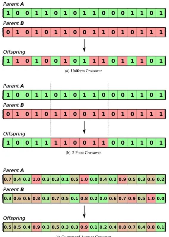
3.3 Examples of Crossover Operations . . . 68
3.4 Example of Non-Dominated Fronts . . . 75
3.5 Extrinsic and Intrinsic Evolution . . . 84
4.1 Screen captures of the MOTIVATEDGUI . . . 93
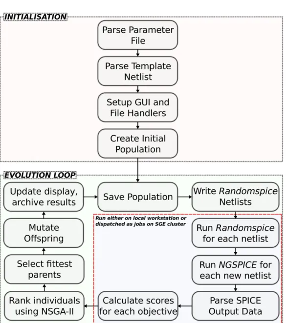
4.2 The workflow of the SGA for Optimising Topologies . . . 96
4.3 Template-Netlist Decoding Example . . . 97
4.4 Test Bench used for most experiments . . . 102
4.5 Input Waveforms for 2-Input Logic Cells . . . 103
4.6 Calculation of delay and slew-rate . . . 108
4.7 Benchmark performance of MOTIVATED. . . 119
4.8 Performance improvement in multithreaded and cluster-based runs . . . 120
5.1 Test bench used in early experiments . . . 122
5.2 Evolved AND and OR Gates . . . 123
5.3 SPICE output from evolved AND and OR Gates . . . 124
5.4 Two stage cycle for optmisation . . . 126
5.5 Test circuits for SCL Optimisation . . . 129
5.6 Uniform stage results for the smaller circuits . . . 132
5.7 Uniform stage results for the larger circuits . . . 133
5.8 Variability in optimised NAND, AND, NOR and OR Designs . . . 135
5.9 Variability in optimised XNOR, XOR and D-Type Designs . . . 136
5.10 Output traces from D-Type circuits . . . 137
5.11 Test bench for multiple voltage source optimisation . . . 140
5.12 Results after uniform stage when optimising voltage-sources only . . . 143
5.13 Results after uniform stage when optimising transistor widths only . . . 144
5.14 Results after uniform stage when optimising widths and voltage-sources . . . 145
5.15 Variability within the multiple-voltage source experiments . . . 147
5.16 CGP Evolved XOR and XNOR Designs . . . 149
5.17 Populations at end of uniform stage for CGP-evolved Designs . . . 150
5.18 Comparison of variability between VSCLIB and CGP-Evolved Designs . . . 151
5.19 Revised cycle for optmisation using HPC Cluster . . . 153
5.20 Detailed study of variability: Buffer . . . 158
5.21 Detailed study of variability: NAND Gate . . . 159
5.22 Detailed study of variability: OR Gate . . . 160
5.23 Detailed study of variability: XOR Gate . . . 161
5.24 Comparison of delay between optimised and reference designs . . . 162
6.1 Workflow for optimisation of larger circuits . . . 165
6.2 Example of Boolean-CGP Genotype and Mapping . . . 166
6.3 Seven-Segment Display Driver Layout . . . 169
6.4 Evolved 2-Bit Adder . . . 172
6.5 Evolved 2-Bit Multiplier . . . 173
6.6 Evolved 3-Bit Adder . . . 174
6.7 Evolved 3-Bit Multiplier . . . 175
6.8 Evolved 7-Segment Display Driver . . . 176
6.9 Test Bench used for Assessing the 2-Bit Multiplier in NGSPICE . . . 179
6.10 Variability in the 2-Bit Adder Circuits . . . 182
6.11 Variability in the 2-Bit Multiplier Circuits . . . 184
2.1 Key product characteristics in ITRS 2009 Roadmap . . . 26
2.2 Lithography Technologies used in CMOS Production . . . 28
2.3 Different distributions of SPICE-based Simulation Software . . . 40
2.4 Revisions of NGSPICE used in this thesis . . . 40
2.5 Performance comparison of SPICE MOSFET Models . . . 42
2.6 RandomSPICE command-line options . . . 49
2.7 Threshold Voltage Variability in a Simulated Device . . . 51
3.1 Differences between Evolutionary Algorithms . . . 69
3.2 Comparison of 1stand 2ndgeneration MOEAs . . . 76
3.3 Examples of Evolutionary Algorithms in Electronic Circuit Design . . . 82
4.1 Mutation Probabilities . . . 100
4.2 List of circuit fitness objectives MOTIVATED . . . 105
4.3 MOTIVATEDRun Parameters . . . 111
5.1 Run parameters in early experiments . . . 123
5.2 Fitness objectives in the two stages of evolution . . . 127
5.3 The run parameters used in the experiments . . . 130
5.4 Number of generations in uniform stage . . . 130
5.5 The run parameters used in the multiple-voltage source experiments . . . 141
5.6 Fitness objectives used in the single-stage optimisation run . . . 154
5.7 The run parameters used in the single-stage optimisation run . . . 155
5.8 Improvement in delay and power for optimised designs over reference designs. 156 5.9 Improvement in delay variability for optimised designs over reference designs. 158 6.1 The 5 test circuits evolved with MO-Boolean-CGP . . . 169
6.2 Run parameters for MO-Boolean-CGP . . . 170 x
6.3 CGP Results Before MO-Optimisation . . . 171
6.4 CGP Results After MO-Optimisation . . . 172
6.5 Comparison of results for evolved and conventional logic designs . . . 181
A.1 VSCLIB Optimisation Results . . . 199
A.2 VSCLIB Optimisation Results Continued . . . 200
A.3 Comparison of SGA, SAHC and SAHC with random walk . . . 201
A.4 Multiple Voltage Source results after variability-stage . . . 202
A.5 Comparisons of results between SCL and CGP Designs . . . 203
The work discussed in this thesis has been developed with Dr. James A. Walker, as part of the nano-CMOS project. Except where explicitly stated otherwise, the bulk of the work discussed in the experiments is setup and developed by myself, with the assistance of Dr. Walker. The development of the MOTIVATEDsystem, described in Chapter 4, has been equally split between the myself and Dr. Walker. Many of the results discussed have previous been described in the published works, detailed below in chronological order. The first-named author for all these papers can be considered the person who conducted the majority of the work in constructing the experiments and writing the papers. All the papers listed have been the subject of a peer-review process, with the exception of the first conference paper which was accepted as a late-breaking paper.
Conference Papers
• James A. Hilder and Andy M. Tyrrell. An evolutionary platform for developing next-generation electronic circuits. In proceedings of Genetic and Evolutionary Computation Conference (GECCO), Late-breaking papers. London, UK, 7–11 July 2007. Pages 2483–2488. ACM.
• James Alfred Walker, James A. Hilder and Andy M. Tyrrell. Evolving variability-tolerant CMOS designs. In proceedings of the 8thInternational Conference on Evolv-able Systems (ICES): From Biology to Hardware. Prague, Czech Republic, 21–24 September 2008. Pages 308–319. Berlin, Germany: Springer.
• James A. Hilder, James Alfred Walker and Andy M. Tyrrell. Optimisation of vari-ability tolerant logic cells using multiple voltage supplies. In proceedings of the IEEE Workshop on Evolvable and Adaptive Hardware (WEAH), part of the IEEE Symposium Series on Computational Intelligence (SSCI).Nashville, TN, USA, 30 March–2 April 2009. Pages 17–24. IEEE Press.
Computation (CEC).Trondheim, Norway, 18–21 May 2009. Pages 2273–2280. Piscat-away, NJ: IEEE.
• James Alfred Walker, James A. Hilder and Andy M. Tyrrell. Towards evolving industry-feasible intrinsic variability tolerant CMOS designs. In proceedings of the 11th Congress on Evolutionary Computation (CEC).Trondheim, Norway, 18–21 May 2009. Pages 1591–1598. Piscataway, NJ: IEEE.
• James A. Hilder, James Alfred Walker and Andy M. Tyrrell. Designing variability tol-erant logic using evolutionary algorithms. In proceedings of the 5thInternational Con-ference on Ph.D Research in Microelectronics & Electronics (PRIME). Cork, Ireland, 12–17 July 2009. Pages 184–187. IEEE Press.
• James A. Hilder, James Alfred Walker and Andy M. Tyrrell. Use of a multi-objective fitness function to improve cartesian genetic programming circuits. In proceedings of NASA/ESA Conference on Adaptive Hardware and Systems (AHS). Anaheim, CA, USA, 15–18 June 2010. Pages 179–185. IEEE.
• James Alfred Walker, James A. Hilder and Andy M. Tyrrell. Measuring the Perfor-mance and Intrinsic Variability of Evolved Circuits. In proceedings of the 9th Inter-national Conference on Evolvable Systems (ICES): From Biology to Hardware. York, UK, 6–8 September 2010. Pages 1–12. Berlin, Germany: Springer.
Journal Papers
• James Alfred Walker, Richard Sinnott, Gordon Stewart, James A. Hilder and Andy M. Tyrrell. Optimizing electronic standard cell libraries for variability tolerance through the nano-CMOS grid. Philosophical Transactions of The Royal Society A: Mathemati-cal, Physical & Engineering Sciences. 2010. Vol 368. Pages 3967–3981.
• James Alfred Walker, James A. Hilder, Dave Reid, Asen Asenov, Scott Roy, Camp-bell Millar and Andy M. Tyrrell. The Evolution of Standard Cell Libraries for Future Technology Nodes. Accepted for publication in Genetic Programming and Evolvable Machines.
The impact of intrinsic-variability within standard-cell designs can be diminished through the optimisation of transistor dimensions using a Multiple-Objective Evolutionary Algorithm. This method can then be combined with other established evolutionary techniques, to create a complete design process for intrinsic-variability tolerant logic circuits, without the need for human designs and intervention.
There are many people whom I wish to thank for their knowledge, support and encouragement throughout my study for this work. Firstly, I must thank my colleague and mentor Dr. James A. Walker, without whom I sincerely doubt that the results presented herein would have been possible - and I also give the greatest of thanks to my supervisor, Prof. Andy Tyrrell, for all the ideas, support and experience he has offered throughout the last four years. I must also mention Prof. Jon Timmis, Mr. Tim Clarke and Dr. Stephen Smith, for their knowledge, support and understanding both before, during and after I began this work.
I would then like to mention everybody else on the nano-CMOS project, and everybody in the Intelligent Systems Group at York, all people I consider friends, with whom it has been a priviledge to have worked with throughout this project. I thank Mr. Thom Blake, Mr. Geoff Burgess and Mr. Gerrard Huck, for being supportive and inspirational housemates with whom I have had the pleasure of living during the last four years. My family, especially my mum, dad and brother, who have always been there when needed, and all my friends. Finally, saving the best till last, I thank Beth, for keeping me fed, watered and sane whilst writing this, without your support I could not have finished this.
Introduction
1.1
Background
The semiconductor industry is a huge global industry, with annual sales now in excess of $250 billion, built on principles of ever increasing power, capacity and speed [6]. For semiconduc-tor companies to produce more powerful microprocessors and more capacious memory chips, it is necessary to periodically shrink the size of components that make up these circuits - the MOS transistors that are assembled in pairs to form the building block logic and memory cells. For many years this reduction in the size of transistors, named device scaling, happened with relative ease, with many technological breakthroughs in the lithographic and fabrication pro-cesses that were needed to create smaller devices. Individual transistors have shrunk from the 10-µm devices that populated Intel’s 4004 microprocessor to 32nm in the cutting-edge devices of today1. Given the atomic radius of a silicon atom is 0.11nm, it is clear that transistors are now approaching a size where they can be considered in terms of their atomic volume instead of traditional dimensions.
In the construction of a transistor, dopant atoms are implanted into the silicon lattice. Whilst the processes are tightly controlled, it is not possible to perfectly control the exact quantity and resting position of these dopants. As a consequence, no two transistors will be exactly the same, which results in differences in the electronic characteristics of each device. Whilst historically these differences have been small enough to be ignored, in recent years the extent of the variations and their random nature has grown to a point whereby transistor variability is now one of the major limiting factors that is curtailing the progression of scaling. Conventional methods to simulate transistors and circuits, and work-flows for creating designs,
1
The figures actually represent the expected DRAM half-pitch - half the distance between cells in a block of dynamic RAM - rather than minimum transistor channel length, which is generally slightly shorter.
do not cater for the effects of variability; within a few years transistors will be scaled to a point where device failure rates and impaired performance will demand drastically different techniques in the design on circuits. Variability can be modelled, but it requires vast three dimensional statistical simulations that consider the electronic flow at an atomic level, which consumes colossal computational resources.
In this thesis, attempts to develop methods which will reduce the impact of this unavoid-able variability are made. A system to attempt to optimise circuits through automatic ad-justment of transistor dimensions within a conventional software simulation package is intro-duced. The optimisation system is based on ideas that come from the world of evolutionary computation, in which algorithms inspired by Darwinian models of evolution are used to ac-celerate the search process.
1.2
The Nano-CMOS Project
The research described in this thesis has formed part of a four-year EPSRC funded project en-titled“Meeting the design challenges of nano-CMOS Electronics”, which is herein known as the nano-CMOS project. The project includes research groups from Glasgow, Manchester, Ed-inburgh and Southampton Universities and also the National E-Science Centre in EdEd-inburgh, in addition to here at the Intelligent Systems Group, within the Department of Electronics at the University of York. The project secured four years of funding from the EPSRC, beginning in October 2006, with substantial further backing from several key industrial partners including Fujitsu, ARM, Wolfson Microelectronics, Freescale, National Semiconductor and Synopsys. The overall goal of the research project is to design accurate models for the simulation of the next generations of MOS transistors devices, focussing primarily on devices in the 45nm - 18nm range. Statistically-based modelling techniques are necessary in the extraction and evaluation of device parameters, as individual transistor elements contain inherent stochastic parameter fluctuations which cannot be removed by refining the manufacturing process.
Device variability is caused by both unavoidable intrinsic parameter fluctuations and also microscopic differences which can occur at many different stages within the silicon manu-facturing process. Accounting for this device variability, through the use of new tools and techniques within the design tool-chains, will add a significant complexity to the overall de-sign process, and will require the coordination of many teams of device experts and the tools they use. A detailed overview of the background to device fluctuations, their causes and the methods used to model them, along with suggested methods of overcoming their implications, is covered in Chapter 2.
The nano-CMOS project is led by the Device Modelling Group within the Electronics De-partment at the University of Glasgow, where sets of statistical models which include intrinsic parameter fluctuations have been developed for devices based on 45nm, 35nm and 18nm tech-nology nodes. The simulations have used both in-house and commercial tools. Libraries of transistor compact models, which can be used in traditional software simulation tools such as SPICE, have been extracted from the analysis of the simulation results. The Microsystems Technology Group at the University Glasgow have worked to develop integrated circuit & de-vice simulators and circuit level compact models using these results. A team at the Electronic Systems Design Group at the University of Southampton have attempted to incorporate the variability statistics higher up the design tool chain by means of extracting behavioural mod-els for standard cell libraries, and a team from the Mixed-Mode Design Group at the University of Edinburgh are developing techniques for using the models to perform noise simulation and circuit level. The variability-aware compact models have been made available on a computing-grid to the Advance Processor Technologies Group at the University of Manchester, who are investigating the impact of device variability on existing design styles (including a large-scale multiprocessor architecture) [21].
A central focus of the whole project is the close involvement with the e-Science commu-nity and the use of cluster-based and Grid computing resources. Grid computing is a special form of parallel computation technology which provides the framework to share processing load across many computers, often distributed at different locations, which are networked to-gether. This allows distributed groups of users to collaborate by sharing not just computing resources, but also designs, work-flows and data-sets, allowing new ways of performing col-laborative research. At the heart of the nano-CMOS project is the development of the prototype of a ‘nano-CMOS Design Grid’, in which each project partner has attempted to grid-enable their code and work flows to allow for the secure and efficient interactions between sites nec-essary for the progress of the overall project. This has been achieved through the nano-CMOS portal2which is the web-based hub for initiating simulations and transferring results, and the use of distributed file-servers based on the Andrew File System (AFS).
1.3
Objectives
The project proposal expressed the ISG’s intended involvement in the project by suggesting three key questions to be answered, all relating to methods in which evolutionary algorithms and associated ideas could be used to assist or improve the modelling of next-generation
de-2
vices, be it within the creation of the models, or in using the models to create improved per-formance of devices and circuits.
• How can evolutionary techniques be used to limit the effects of parameter variations?
• How can evolutionary techniques be used within device models to alleviate parameter fluctuation problems?
• How can parameter variation datasets be best used by evolutionary techniques to im-prove system performance?
Over the course of the four year project, the research at York has primarily focussed on addressing the first question above, although all three questions have been addressed in some capacity, as is discussed in the conclusions of this thesis. Two separate routes have been inves-tigated in an attempt to find solutions to the first question. Dr. James Walker has focussed on investigating if the use of evolutionary techniques, notably a reworking of Cartesian Genetic Programming, could be used to design novel topologies of logic cells, which offered improved performance over conventional designs when subjected to the effects of transistor variability. I have attempted to reduce the impact of variability through the optimisation of transistor dimen-sion within conventional and evolved standard cells through the use of a Genetic Algorithm. This has been followed with an investigation to see if other established evolutionary techniques can be combined in a design flow to create completely novel variability tolerant circuits. As such, the following statements can be considered the hypothesis which the research presented in thesis attempts to prove:
The impact of intrinsic-variability within standard-cell designs can be diminished through the optimisation of transistor dimensions using a Multiple-Objective Evolutionary Algorithm. This method can then be combined with other established evolutionary techniques, to create a complete design process for intrinsic-variability tolerant logic circuits, without the need for human designs and intervention.
1.4
Structure of Thesis
The thesis is organised as follows. Chapter 2 provides a detailed overview of the problem of transistor variability. This commences with a description of the MOS transistor and its physical operation, including the processes involved in creating large scale integrated circuits. An analysis of the different causes and consequences of device variability is then given, fo-cussed on the stochastic variations caused by atomic level differences. This is followed by descriptions of the systems used to model variability and simulate transistor-based circuits, emphasising the tools that are used in this thesis. The chapter concludes with a look a the consequences of variability on logic design and what potential solutions exist to surmount the issues.
Chapter 3 gives an outline of the field of evolutionary computation, looking at the history and operations of the main types of evolutionary algorithms, including a detailed analysis of multi-objective optimisation techniques which are used in this research. A summary of some of the major developments of evolutionary techniques applied to field of electronic engineering is given at the conclusion of the chapter.
Chapter 4 introduces the framework of tools that have been developed to combine the variability-aware compact models, described in Chapter 2, with the multi-objective evolution-ary algorithms discussed in Chapter 3. This includes a detailed description of the Simple Genetic Algorithm, which is used to optimise transistor dimensions within standard cell li-braries.
The application of the algorithm is covered in Chapter 5, which discussed the results ob-tained when applying the algorithm to different sets of publicised libraries of cells. The de-velopments made to the system throughout the course of the experiments are discussed, with comparisons to other optmisation techniques given.
Chapter 6 proposes the development of evolution inspired algorithms further into the logic design framework, by means of combining the optimisation techniques discussed in Chapters 4 & 5 with a system for creating logic topologies at a block-level. This aims to create the beginning seed of a system by which large logic designs can be completely evolved and opti-mised without the need for traditional design methods. Concluding remarks and observations are given in Chapter 7.
Transistor Variability
2.1
Introduction
Complimentary Metal-Oxide Semiconductor (CMOS) form the backbone of almost all mod-ern digital circuits. The first example of integrating multiple components on a monolith of semiconductor was demonstrated by Jack Kilby in 1958 [83]. The first CMOS based devices were assembled by Fairchild Semiconductor in 1963 [174], with the first commercial CMOS integrated circuits, the ‘CD4000’ series, released by RCA in 1968 [107]. The vast majority of very large scale integration (VLSI)1 circuits are assembled from CMOS-based logic, includ-ing microprocessors, programmable hardware such as FPGAs, memory and many other types of circuits. Designs are build using complementary, symmetrical pairs of p-type and n-type MOSFETs arranged to create logic and memory functions.
The semiconductor industry itself is built upon the principles of CMOS devices increasing in complexity and performance with each product generation. The physical sizes of die (the functional block of the integrated circuit as fabricated on silicon) are fundamentally limited by the physical properties of the silicon wafer and economic constraints; thus in order to achieve increasing complexity, the dimensions of individual transistors have to periodically shrink. Transistor have now shrunk to a point where their construction can now be considered in terms of atoms instead of conventional dimensions, however it is not possible to guarantee the atomic layout and structure of any two transistors will be identical. The atomic variations between transistors results in significant differences in their operating characteristics, which creates new problems in the design, simulation and operation of large circuits which are not
1
VLSI is herein used to describe all integrated circuits with upwards of one hundred thousand devices. This includes ultra large scale integration (ULSI), with tens of millions of devices per chip, and gigascale integration (GSI), with billions of devices per chip [113].
currently solvable using conventional design techniques.
In this chapter the causes, effects and potential solutions to the problem of atomic-level variability in transistors are considered. The chapter begins with a background overview of the MOSFET transistor, the key building block in created large scale integrated circuits. The structure and basic operation of the MOSFET are reviewed based on the traditional circuit models and theory. The process of utilising MOSFETs to create integrated circuits is then discussed, with the basic building block cells required to make CMOS logic gates and an overview of the steps in the manufacturing process of a CMOS integrated circuit, from wafer through to packaged device. A review of the history and proposed future of transistor scaling is then discussed, followed by a detailed analysis of the different types of transistor variability which occur in modern and future devices, focussed on the atomistic variabilities on which the work in this thesis is based. The following section is an overview of the techniques used to simulate circuits incorporating the effects of variability. The chapter concludes with a synopsis of the specific problem areas of device variability in modern logic and potential solutions to overcome the issues.
2.2
The Metal-Oxide Semiconductor Field-Effect Transistor
The Metal-Oxide Semiconductor Field-Effect Transistor (MOSFET) is a four-terminal device, available with either ann-type or ap-type channel. It is often used in pairs to form digital oper-ations, and it is also used extensively in modern analogue circuits as current sources, voltage-controlled resistors and for power switching. Unlike a bipolar junction transistor (BJT), in which the output current is controlled by the input current at the base terminal, the FET con-trols output current based on the input voltage at the gate terminal. Field-effect transistors exist as both Junction FET (JFET) and Insulated-Gate FET (IGFET); the MOSFET is a type of IGFET where the metal gate electrode is electrically insulated from the substrate via a thin layer of silicon oxide.The schematic symbols for the main types of MOSFET transistors, along with their asso-ciation voltage and current definitions, is illustrated in Figure 2.1. The substrate connection in a FET, often labelled asBorbulk, in most often connected to the source; in many devices this connection is made internally, hence both the schematic and packaged device are often seen with only three terminals.
In a MOSFET transistor, the drain current ID is controlled by the gate-source junction
Figure 2.1: Four-terminal schematic circuit symbols for enhancement and depletion mode MOSFET transistors gm= ∆ID ∆VGS (2.1) Transconductance gm is measured inmhoorSiemens, although with ID typically being
measured in the range ofµA or mA, it is more common to find values represented in terms of millisiemens (mS). MOSFETs are available which cover a vast range of power handlings, with large discrete devices able to sink several hundred Watts, and the very low gate-leakage makes them suitable for numerous applications [79].
2.2.1 Structure of Field-Effect Transistors
The structure of a typical NMOS and PMOS transistor illustrated in Figure 2.2. In a fabricated CMOS circuit, a lightly dopedp−silicon is used as the device substrate, allowing a n-channel device to be directly formed with two heavily dopedn+regions; a p-channel device requires the creation of an additional lightly dopedn−well, as can be seen in Figure 2.2b. The heavily doped regions form the Source and Drain connections, with the gate electrode separated by a thin layer of oxide.
(a) NMOS Transistor (b) PMOS Transistor
Figure 2.2: Physical cross-sectional structure of a NMOS and PMOS transistor, based on illustrations from [154, 160]
Early MOS transistors were built with a metal gate electrode (typically aluminium) on top of an oxide insulating layer on top of a semiconducting substrate. More recent designs replaced the metal gate electrode with one made from a polycrystalline silicon material which can tolerate the high temperatures in the annealing process better (although the name MOS has been retained). Some of the most recent design have an insulating layer with a high dielectric constant (known as high-κmodels) have reverted back to using a metal layer as the gate electrode. To improve the performance in terms of speed and power consumption, the scaling of individual components is reduced allowing it to operate at a faster speed or with lower power wastage.
2.2.2 Function of Field-Effect Transistors
The basic function of a MOS transistor can be evaluated by considering the behaviour of a n-MOS device under different conditions. With all terminals grounded, the source and drain electrodes are separated by a pair of back-to-back P-N junctions, resulting in a very high resistance; the gate and substrate form a capacitor with theSiO2 acting as a dielectric. If a
negative voltage is applied to the gate, negative charges will accumulate in the poly-silicon gate and increased positive charges will be attracted to the channel. If either the source or drain are then given a positive-bias, only a negligible current will flow between them; this is the leakage current of the device.
When a positive potential is applied between the gate and source (VGS), holes are repelled
away from the substrate-oxide interface which results in a depletion region. An increase in the gate voltage results in negative charges being attracted to the channel; once enough exist the channel will change from being ap−region to anregion and is said to be inverted. The gate-source voltage at which this inversion takes place (i.e. when the concentrations of electrons under the gate equals the concentration of holes deep in the p− substrate is the transistor threshold voltage,VT. In the simplest approximation, whenVGSis belowVT no current flows
between source and drain - the device is in its cut-off region. IfVGS is aboveVT, the channel
electrically joins source and drain and current can flow freely [15].
Clearly this is an over-simplification; in reality whenVGSis close toVT a gradual change
of charge occurs in the channel, resulting in small current flow from source to drain; the device is considered to be in ‘weak inversion’ and working in the sub-threshold region.
MOSFET as a capacitor
In a condition where the channel is present, the accumulated negative charge is proportional to VGS and is dependant on the oxide-thicknesstox with the transistor operating as a capacitor.
The gate capacitance per unit area is defined as follows: Cox =
ox0
tox
(2.2) in which 0 is the permittivity of free space, ≈ 8.854×10⁻¹² Fm−1, and ox is the
relative permittivity ofSiO2,≈3.9. The total capacitance of the device can be calculated by
multiplying equation 2.2 by the device area:
Cgs=W LCox (2.3)
This allows the charge in the device channel to be calculated as follows:
QT =Cgs(VGS−VT) (2.4)
MOSFET as a resistor
An increase inVD allows a current to flow between drain and source through the channel.
WhenVDis of a small value well belowVT, the charge-density in the channel will not increase
significantly. The device effectively operates as a resistor of lengthLand width W, which relates the drain-source currentIDS and voltageVDS based on the gate voltage as follows:
IDS=µnCox(VGS−VT)
W
LVDS (2.5)
MOSFET in linear region
AsVDincrease, the charge density profile across the channel changes. It is generally assumed
to be a linear gradient between source and drain, which results in a revised equation to relate IDS toVDS; the current follows a linear relation toVGSand a quadratic relation toVDS[15]:
IDS =µnCox VGS−VT − VDS 2 W LVDS (2.6)
MOSFET in saturation region
OnceVD is increased the point where the drain-gate voltageVDGequals threshold voltage
VT, the charge density in the channel adjacent to the drain becomes zero and consequentially
the currentID approaches its maximum value; the transistor is said to be in saturation region.
The charge concentration in the channel can be approximated as being constant beyond this point, which allows a new current expression to be derived. Given thatVDG≥VT andVDS =
VGS+VDG, we can define a conditionVDSsat =VGS−VT. ReplacingVDSwithVDSsat in
equation 2.6 yields the saturation region current equation: IDS =µnCox(VGS−VT)2
W
2L (2.7)
In reality a further increase inVDresults in an effect named channel length modulation, in
which the channel length is decreased and the pinch-off region is increase. To account for this effect, a revised saturation region current equation incorporates a modulation factorλwhich is inversely proportional to channel lengthL, as shown:
IDS =µnCox(VGS−VT)2
W
2L[1 +λ(VDS −VDSsat)] (2.8)
WhenVDS increases well beyondVDSsatthe device can enter a condition known as
break-down, in which current can increase dramatically withVDS. The causes of device breakdown
differ between short and long channel devices; in the former it is a breakdown of the par-asitic bipolar transistor formed whilst in the latter it is a breakdown of the drain-body p-n junction [42].
Body-Effect
All the previous equations have assumed the substrate connection is connected to the source; this is certainly the most common form of operation, but is not a prerequisite condition. Where the source and substrate are at different potentials, a number of second-order effects exist which are named ‘body effect’; this can be modelled as an increase in threshold voltage, as shown in the following formula derived by Gray and Meyer, in which VSB is the
source-substrate potential andVT ,n0is the threshold voltage with zeroVSB [69].
VT,n=VT ,n0+γ p VSB+ 2|φF| − p 2|φF| (2.9)
Figure 2.3: Cross-sectional structure of a NMOS transistor in saturation mode highlighting the parasitic capacitances [160, 15]
Parasitic Effects in a MOS Transistor
A MOS transistor in the saturation region includes several parasitic capacitive effects, which are illustrated in the cross-sectional model shown in Figure 2.3. The most significant effect oc-curs from the capacitors formed between the gate and source of the device; these are depicted in the diagram asCg:chandCg:soverlap. The capacitor formed between the gate poly-silicon
and the channel can be approximated to a linear capacitor dependant on the device area and oxide thickness, which roughly equates to: [136]
Cg:ch ≈
2
3W LCox (2.10)
There is an additional contribution from the capacitance that occurs in the narrow overlap between the gate and then+doped source region, which results from horizontal spreading of the dopant during the fabrication process. Considering the length of the overlap to beLoverlap
the resulting parasitic capacitance is equal to:
Cg:soverlap =W LoverlapCox (2.11)
Equations 2.10 and 2.11 can be combined to give a gate-source capacitanceCg:s as
fol-lows: Cg:s≈W 2 3L+Loverlap Cox (2.12)
ca-pacitance:
Cg:d=Cg:doverlap =W LoverlapCox (2.13)
The other parasitic capacitances occur between at the interfaces between the source, chan-nel and drain regions with the substrate and field-implant regions. The most significant are Cs:b, and Cd:b, formed by the depletion regions which occur at the reverse-biased p-n
junc-tions at the source and drain. IfLef f is the defined as the length of the n+ source and drain
regions, the capacitances can be calculated as follows [160]: Cs:b,d:b =
W Lef f
(1 +VD,S/Φb)M J
×CJ (2.14)
whereΦbis the working potential of the bulk, andM JandCJare process-dependant
con-stants. The capacitances between the source and drain regions with the field-implant regions are considered to beside-wall effectsand can be calculated as follows:
Cs:bsidewall,d:bsidewall =
W + 2Lef f
(1 +VD,S/Φb)M Jsidewall
×CJsidewall (2.15)
In addition to the parasitic capacitances, there are additional resistances and leakage cur-rents which must be considered. There are ohmic resistances at the source and drain connec-tions, typically of the order of10Ωfor VLSI CMOS, which become significant in high-drain current applications. Leakage currents exist between the source & drain regions and the sub-strate bulk, which can be approximated by reverse-biased diodes using the Shockley ideal diode equation [160]: IBD,BS =Is e qVBD,BS kT −1 (2.16) whereqis the elementary charge,1.602×10−19C,kis the Boltzmann constant,1.381×
10−23JK−1,T is the temperature in Kelvins andIs is the reverse saturation current of a P-N
junction.
2.2.3 Structure of CMOS Integrated Circuits
Almost all modern VLSI (very large scale integration) circuits are assembled from CMOS based logic, including microprocessors, memory and many other integrated circuits. Most devices are built upon complementary, symmetrical pairs of p-type and n-type MOSFETs to create logic functions. CMOS is widely used in modern devices as it possesses low static power-supply drain and high noise immunity, with significant power only being drawn when
the transistors are in a transitional state (switching between on and off states). This allows CMOS logic circuits to be built with far lower power consumption (and consequentially less heat production) than other traditional logic designs such as TTL.
Early CMOS devices were significantly slower than equivalent TTL (transistor-transistor logic) devices, although the low-power consumption led to their inclusion in early digital watches where battery life was more important than processing speed. For many years CMOS logic devices were built to be tolerant of a wide range of supply voltages, allowing them to interface easily with TTL with its industry-standard 5 volt power supply. By the early 1990’s the desire to increase circuit density and speed led to a drop in CMOS supply voltages and the continued reduction of the geometric dimensions of devices. The most modern CMOS devices have been built to operate from supply voltages of 1 volt or less, with gate lengths for individual transistors now well under 100nm [154].
Much of the current research and development within the semiconductor industry is con-cerned with the development of System-on-a-Chip (SoC) technologies, which involves the in-tegration of high-performance CMOS log and embedded memory (both SRAM or DRAM for convention, volatile random-access, alongside EEPROM or FLASH as long-term non-volatile storage), along with analogue CMOS components for base-band functions and RF-BiCMOS for mobile-radio and tuner functions. BiCMOS combines bipolar devices with CMOS devices, allowing for increased speed and drive currents in specific applications. To allow for both the high-integration density and high performance, it is necessary to continually scale down the size and operating voltages of the CMOS components.
2.2.4 Dielectric Materials
The traditional dielectric material used in the creating of CMOS devices has been silicon diox-ide (SiO2). As devices have become smaller, the thickness of this dielectric layer has steadily
decreased, which naturally leads to an increase in gate capacitance; this has the effect of im-proving drive current and overall device performance. However, recent technology nodes have seen the width of the dielectric layer reduce to below 2nm, which has resulted in a dramatic increase in leakage current. This is due to quantum tunnelling, a quantum mechanical phe-nomenon observed where a particle passes through a barrier despite have a lower mechanical energy than the potential energy of the barrier [137]. The effect of this increased leakage current results in a increased overall power consumption of the device, and consequentially a reduced device reliability.
The gate-oxide layer of a MOSFET device can be modelled as a plate capacitor, the value of which is dependant on the area of the layer, the thickness of the layer, and the relative
di-electric constant of the materialκ. Ignoring any quantum mechanical and depletion effects, the capacitance of the layer is given in Equation 2.17, in whichAdenotes the capacitor area,tis the thickness of the oxide layer and0in the permittivity of free space (8.854×10⁻¹²F m−1).
C= κ0A
t (2.17)
To increase the gate capacitance, the options are either increasing the dielectric area, re-ducing the thickness of the dielectric, or increasing the dielectric constant of the material. Increasing the area negates advantages obtained in the shrinking of the technology; reducing the oxide-layer thickness results in unmanageable leakage current as described before. There-fore modern devices have turned to attempting to overcome these limitations with the use of a high-κdielectric material. In such devices, the layer thickness is often increased over itsSiO2
equivalent as a means of reducing leakage current (and increasing device reliability) whilst maintaining a similar overall capacitance.
2.2.5 The CMOS Fabrication Process
In order to understand the causes and effects of transistor variability that occurs in CMOS, it is necessary to have a degree of understanding of the fabrication process that occurs. This section briefly describes the steps taken to convert raw materials in a packaged integrated circuit. Growth of Silicon Ingot
The first stage in the fabrication process is the growth of a large, cylindrical ingot of single-crystal silicon, based on a method discovered by Jan Czochralski in 1916. High-purity silicon is melted in a quartz crucible in a controlled environment, with an argon atmosphere. A seed crystal is dipped into the molten silicon, and with a high degree of precision is slowly rotated and retracted, in a process commonly known as Czochralski pulling [43]. A tightly-controlled addition of dopant atoms, typically boron or phosphorus (although arsenic and antimony are also used) can be added to the molten silicon mix to create n-type or p-type doped silicon. Throughout the history of semiconductor fabrication, the ingots have periodically got wider and longer, with most major manufacturers currently producing 200-mm and 300-mm wide ingots, and 450-mm fabrication plants likely to appear around 2012 [2]2. A number of tech-nical problems need to be overcome for each step in wafer-width, with 450-mm ingots set to be 3 times heavier than their 300-mm equivalents, approaching 1000kg per ingot, and twice as
2The 2009 ITRS roadmap has set the date for introduction of 450mm wafers between 2014 and 2016, noting
long to grow and cool, resulting in significantly increased process times. Other techniques to Czochralski pulling are used for certain types of devices, such as the float-zone technique for power devices and the Bridgman-Stockbarger technique, used in gallium-arsenide and other non-silicon semiconductor growth [16].
The grown ingots, which can be in excess of 1 meter in length, are then sliced into wafers using multi-wire wafer saws or electrical-discharge machinery techniques [162]. The resultant wafers are generally between 275µm and 1000µm in thickness, with 300 mm ingots generally being sliced to 775µm thickness wafers, and forthcoming 450 mm ingots likely to be 925µm in thickness [2]. The wafers are polished to ensure an even width and cleaned with weak acid solutions to remove any unwanted particles and damage caused by the sawing process. Oxidation
The first step in processing the cleaned wafer is that of the growth of the layer ofSiO2 on
the surface; the oxide layer grows both into the silicon and as above the original surface, with approximately 44% of the total oxide-width formed below the surface. The oxide layer is most often accomplished through a process named thermal oxidation, in which controlled high temperatures (typically between700◦Cand1300◦C) promote the growth of theSiO2. This
takes place in an oxidation furnace, in which the wafers are placed in quartz ‘boats’ with the oxidising agent diffusing over the surface of the wafer at atmospheric pressure. The oxidising agent is eitherO2in dry oxidation, orH2O(steam) in wet oxidation; dry oxidation is preferred
as it results in fewer defects [154, 1, 16]. Diffusion and Ion-Implantation
Diffusion and Ion-Implantation are the two processes in which dopant atoms are introduced into the silicon wafer; diffusion was used extensively in IC fabrication in the past but for high-density CMOS circuits ion-implantation is now more commonly used. In the diffusion process, impurity atoms which are at the surface of the wafer are moved into the bulk of the material under high temperatures, between800◦Cand1400◦C, in a diffusion furnace.
In the ion-implantation process, ions of a particular dopant are accelerated by an elec-tric field and physically lodge within the silicon substrate. The typical depth of penetration varies between 0.1µm and 0.6µm, dependant on the angle and velocity at which the ions strike the wafer. Ions are implanted off-axis from the wafer to ensure they experience colli-sions with lattice atoms, avoiding a ‘channelling’ of ions deep in the silicon. The process of ion-implantation causes damage to the crystal lattice of the silicon, which results in certain numbers of the implanted ions being electrically inactive. These inactive ions are recovered
through the process of annealing, in which the wafer is heated to roughly800◦C, which al-lows the implanted ions to move to electrically active locations within the lattice, although the annealing process can lead to some unintended diffusion of the dopants; this can be minimised through careful optimisation of the annealing time and temperature [112, 16].
Ion-implantation is generally preferable to diffusion in the creation of modern silicon in-tegrated circuits as it allows a greater precision in the control of doping concentrations as the current of the ion-beam can be accurately measured during implantation; doping concentra-tions can be controlled to within±5%. It also has the advantage of being a room-temperature process (except for the annealing process), and the ability to implant through a very thin oxide layer; the diffusion process requires that the surface be free ofSiO2. The final advantage is
a greater control over the depth-profile of implanted dopants; if needed, a concentration peak can be placed well below the surface of the silicon [154].
Deposition
At different stages in the fabrication process, thin films of dielectrics, semiconductors and metals have to be deposited on the silicon wafer. Several different techniques for deposition exist, including sputtering, evaporation and chemical-vapour deposition (CVD). The process of sputtering involves placing the wafer on an anode within a vacuum, with a cathode coated in the material to be deposited. Positive ions are bombarded against the cathode by means of a strong DC, radio-frequency or magnetic field, which results in the target material being dislodged onto the wafer through the process of direct momentum transfer. In the evaporation-deposition process, a solid material is heated within a vacuum until it evaporates. The evapo-rated molecules then strike the cooler surface of the wafer, condensing into a solid film on the surface [16].
The CVD process operates by way of reacting a silicon-rich gas such asSiH4 with an
oxygen-rich precursor which results in a chemical reaction, depositingSiO2 on the substrate.
The process can be occur at low-pressure in LPCVD, or at high-pressure in plasma-enhanced (PECVD) systems. Unlike the thermal oxidation process, CVD can occur at relatively low temperatures and does not consume any of the silicon from the surface of the wafer; the process of CVD can also be used to deposit other dielectric materials on the surface, including the polycrystalline silicon frequently used in modern devices and silicon nitride (Si3N4) [154].
Photolithography
Photolithography is the process that creates the complex patterns used to isolate the positions of different device areas on the completed silicon wafer; it refers to the complete process of
taking a circuit image, invariably created on a computer, to creating aphotomask, and trans-ferring it to the wafer. The first stage of the process is the creation of a transparent quartz plate which contains the required pattern, called areticle. The reticle is coated with a UV-light absorbing layer, typically iron-oxide, then further coated with a thin layer of electron-beam resist - an organic polymer which chemically changes when exposed to energetic particles. A computer controlled electron-beam exposes the resist layer selectively based on the desired patterns. The reticle is then developed in a chemical solution which removes the unwanted ar-eas. Two main types of photoresist exist: positive-resist, in which exposed areas are removed, and negative-resist in which unexposed areas are removed. A plasma then etches off the un-coated areas of iron-oxide, leaving the patterned reticle. Many different reticles, often over a dozen, are needed throughout the fabrication process, each corresponding to the patterns required at different process steps. The reticle will typically contain the pattern for a single die as opposed to the entire wafer, and is scaled many times larger than the desired pattern to be created, being reduced and repeated several times to create the complete image across the wafer.
To transfer the image from the reticle onto the silicon wafer, the wafer is first coated with a thin ( 0.5µm) uniform coating of a UV-sensitive photoresist, deposited by spinning the wafer rapidly at≈3000rpm. An ultra-violet lightsource is focussed through the reticle and a reduction lens onto the wafer, causing exposed regions to become acidified. Different photoresists and lightsources determine the minimum feature size that can be created; these are discussed in greater detail in Sections 2.3.3 and 2.5.2. The exposed wafers are developed in a Sodium Hydroxide solution, which etches the exposed photoresist away, then cured by baking at roughly125◦Cto harden. Complete wafers are exposed in a die-by-die basis using a step-and-repeat process, which utilises laser controlledmask alignersfeaturing a very high degree of precision. The complete process of photolithography, including the techniques used, the chemicals used for photoresist and the exposure methods used to create the masks and features on-wafer are critical to the scaling process, and can themselves lead to variability in produced devices, as will be discussed later [16, 154].
Etching
Etching is the process of removing the unwanted material after the photoresist pattern has been formed. The etching process can be characterised by two desirable characteristics:selectivity
andanisotropy. Selectivity is the ability of the process to remove just the desired area, leaving the masked areas and underlying substrate intact. Anisotropy is the ability to etch in one direction, and one direction only. Neither can be perfectly achieved; any etching process will
result in some degree of removal of undesired areas and some degree of undercutting [16]. Originally etching was a wet process, using a dilute Hydrogen Fluoride solution to remove areas ofSiO2. Hydrofluoric acid has strong selectivity - it is very effective at removing the
oxide whilst leaving the silicon substrate and photoresist-covered areas intact; unfortunately it etches isotropically, meaning it removes the oxide as quickly laterally as it does vertically, etching the oxide beneath the photoresist too much to cope with modern feature sizes. Other wet etching processes exist to remove other unwanted areas: phosphoric acid for metal areas, nitric acid for poly-silicon and phosphoric acid for silicon nitride, although for modern sub-micron processes a dry etching process is generally used to avoid the undercutting effect [154, 16]. Additionally, dry etching is a cleaner process, negating the need to carefully remove the acidic residue, it also offers greater compatibility with vacuum-processing techniques such as molecular-beam epitaxy, and is generally easier to automate [112].
Modern CMOS manufacture uses a plasma-based dry etching process named Reactive-Ion Etching (RIE). An etch-gas is pumped into a chamber, in which an RF voltage accelerates the electrons to high kinetic energies. Collisions between the electrons and neutral atoms creates ions and radicals; the ions are bombarded onto the wafer normal to the surface, ensuring an anisotropic etch, whilst the radicals simultaneously create a very selective isotropic etch. The resultant etch is thus a compromise of selectivity and anisotropy, allowing smaller feature sizes than could be manufactured with wet etches [154].
Metallisation and back-end processing
Once the semiconductor devices are fabricated, interconnections and contacts for wire-bonds are created through the process of metallisation. For silicon substrates, an aluminium alloy (typically 95% Al, 4% Cu and 1% Si) is deposited using the sputtering process. The alu-minium is then patterned and etched using RIE, before being sintered at roughly450◦C to ensure a good ohmic contact with the silicon. A protective overcoat of silicon nitride is then deposited using chemical vapour deposition [16]. Pure aluminium is unsuitable for metalli-sation in VLSI CMOS because of electromigration effects (changing shape when subject to currents) and junction spiking; the silicon-aluminium commonly used to alleviate these prob-lems leads to a high contact resistance, which is undesirable with the minute contacts formed in submicron devices; this has lead to the study and use of other materials, notably copper, as interconnects in modern devices [55].
The wafer now contains a quantity of complete die; the next step in the process is to divide up the wafer using a saw or scribe into individual circuits, mount the devices in the appropriate packages, and apply gold or aluminium bond wires between the aluminium contact points and
the package leads; this is phase is known as back-end processing. Fabrication steps for n-well Silicon
To illustrate how the above processes are combined in the creation of integrated circuits, a step-by-step outline is given in Figures 2.4 & 2.5. These diagrams show the steps to create transistors on the silicon wafer for the n-well silicon-gate CMOS process, one of the most frequently used in modern devices. A real-world GSI device would likely have many more steps and metal layers than are shown in the diagrams due to the scale of the device and complexity of interconnections.
2.2.6 Transistor Sizing
The sizing of transistors within a logic or memory circuit is a key area of optimisation in CMOS design. The size dictates critical circuit parameters, such as delay, energy consump-tion and fan-out. The sizing determines the dynamic energy consumpconsump-tion through means of changing the switched capacitances, and also the leakage current of the circuit; it also affects energy consumption by determining the minimum operating voltage at which the circuit can correctly function [63].
The three major sources of power dissipation are summarised by Chandrakasan et al in Equation 2.18 [39]. The first term is the dynamic or switching component, the product of loading capacitanceCL, supply voltageVdd, voltage swingV and the clock frequencyfclk;pt
is the activity factor, the probability of a power-consuming transition occurring3. The second term is the leakage currentIleakagewhich arises from sub-threshold effects and substrate
in-jection. The final term is the short-circuit currentIsc which occurs when NMOS and PMOS
transistors are simultaneously active, creating a direct path from supply to ground; this is gen-erally a factor of static designs and is gengen-erally avoided in dynamic logic, except for when static pull-up devices are used, or a significant clock skew is present. It is clear that signifi-cant dynamic power improvement can be gained through the use of low-threshold devices and minimising supply voltages, however, this has the general trade-off of increasing sub-threshold currents causing a rise in static power dissipation.
Transistor sizing in a fabricated circuits is governed by a set of criteria known as design rules; these rules are a list of process-specific critical geometrical size and spacing constraints that must be adhered to when designing the lithographic masks, originating from limitations imposed by the lithographic process and physical constraints [163].
3
The voltage swing is generally the same as supply voltage, thus switching power is generally proportional to
(a) The first step of the process is the growth of a thin
SiO2oxide layer on the surface of a lightly p−doped
wafer.
(b) The n-well is created by first depositing and devel-oping photoresist around the area to be masked, then subjecting the wafer to a n−implantation. The pho-toresist is then removed and a high-temperature drives the implanted ions into the substrate.
(c) A layer of silicon nitride is deposited over the en-tire wafer. Another layer of photoresist is deposited and developed on the silicon nitrite in areas where de-vices will reside, known asmoats.
(d) The silicon nitrite is removed from the other areas. A global n−-type field is implanted to these areas to ensure parasitic p-channel devices are not accidentally turned on via interconnect lines.
(e) The photoresist is removed then the process is re-peated with a p−-type field to ensure n-channel de-vices are not turned on.
(f) A thickSiO2field oxide is the grown over the
en-tire wafer in all areas except whereSi3N4resides. The
oxide grows under the edges of the silicon nitride, re-sulting in the‘bird’s beak’shaped field-oxide regions.
(g) TheSi3N4is removed and the whole wafer is
cov-ered with a very thin layer ofSiO2; this forms the gate
oxide of the transistors. A thicker poly-silicon layer is then deposited over the entire wafer.
(h) The poly-silicon is patterned and etched where transistor gates and interconnect lines are needed. A
SiO2 layer is then grown over the poly-silicon and
anisotropically etched, leaving thin oxide spacers on either side of each gate.
(i) To create the n-channel devices, photoresist is ap-plied to mask unwanted areas, thenn+ ions are im-planted into the substrate in areas not protected by pho-toresist, field oxide, poly-silicon and oxide spacers to create the source/drain regions.
(j) The oxide spacers around the poly-silicon gate of the n-channel transistors are then etched away, fol-lowed by a lightern−implantation, to create a lightly-doped region.
Figure 2.4: The early fabrication steps involved in constructing an n-Well CMOS Circuit (continued on next side).
(a) The lightly doped drain and source regions created by then−implantation can be seen in this figure. This area of higher resistivity close to the poly-silicon gate helps to minimise impact ionisation. The photoresist is removed.
(b) The previous steps are then repeated to create the p-channel devices; photoresist is applied to mask the n-channel devices, an successivep+ andp− implan-tations are applied to create the p-channel drain and source with lightly doped regions.
(c) With the transistors now created, the process of ter-minating contacts and interconnect the devices begins. A thick layer of oxide, typically borophosphosilicate glass (BPSG) is deposited.
(d) The BPSG in areas where contacts are needed is etched away. A layer of aluminium is deposited on the surface, forming contact with the relevant poly-silicon areas, and unwanted aluminium areas are etched away.
(e) A thick dielectric area is applied before the sec-ond layer of metals. This is typically a sandwich of
SiO2 applied with chemical-vapour deposition,
fol-lowed by a spun-on layer of glass, folfol-lowed by a final CVDSiO2 layer, to minimise stray capacitance and
ensure planarity.
(f) The vias (inter-metal connections) between the metal layers are isolated with photoresist and etched, before a second metal layer is deposited over the whole wafer.
(g) The second metal layer is selective etched to leave only the wanted interconnect regions. A thick layer, usually SiN3, known as the passivation protection
layer, is applied over the entire surface of the wafer. The areas where contacts are needed are etched from theSiN3 and a final layer of metal is deposited and
selectively etched.
(h) The wafer is split, individual die are packaged and wires are bonded from the relevant contacts to pins on the package. It should be noted that a modern IC may have many more metal layers, each separated by dielectric-sandwich layers, than pictured here, and that the bond wires, whilst often smaller than 15µm, are much larger than device channels.
Figure 2.5: The later fabrication steps involved in constructing an n-Well CMOS Circuit. Based on [16, 154].
![Figure 2.2: Physical cross-sectional structure of a NMOS and PMOS transistor, based on illustrations from [154, 160]](https://thumb-us.123doks.com/thumbv2/123dok_us/10101600.2910640/27.918.131.748.813.959/figure-physical-cross-sectional-structure-nmos-transistor-illustrations.webp)
![Figure 2.3: Cross-sectional structure of a NMOS transistor in saturation mode highlighting the parasitic capacitances [160, 15]](https://thumb-us.123doks.com/thumbv2/123dok_us/10101600.2910640/31.918.157.730.188.377/figure-sectional-structure-transistor-saturation-highlighting-parasitic-capacitances.webp)
![Figure 2.7: The maximum clock-speeds and core-counts of various Intel Microprocessors at different release dates [77, 5]](https://thumb-us.123doks.com/thumbv2/123dok_us/10101600.2910640/45.918.152.705.162.443/figure-maximum-speeds-counts-various-microprocessors-different-release.webp)
![Figure 2.8: The main types of intrinsic variability illustrated on a 3D-simulated model of a 35nm MOSFET device [22]](https://thumb-us.123doks.com/thumbv2/123dok_us/10101600.2910640/49.918.159.718.165.406/figure-types-intrinsic-variability-illustrated-simulated-mosfet-device.webp)
![Figure 2.9: The atomic structures of 22nm and 4nm stylized transistors illustrating random discrete dopant placements [22]](https://thumb-us.123doks.com/thumbv2/123dok_us/10101600.2910640/50.918.189.796.170.427/figure-atomic-structures-stylized-transistors-illustrating-discrete-placements.webp)
![Figure 2.13: A hierarchical simulation methodology necessary to capture the impact of intrin- intrin-sic variability on design [151].](https://thumb-us.123doks.com/thumbv2/123dok_us/10101600.2910640/69.918.130.739.168.542/figure-hierarchical-simulation-methodology-necessary-capture-impact-variability.webp)
![Table 2.7: Threshold Voltage Variability caused by Intrinsic Parameter Fluctuations in a 35 × 35 nm Atomistic-Simulated Device [139]](https://thumb-us.123doks.com/thumbv2/123dok_us/10101600.2910640/70.918.194.778.220.582/threshold-voltage-variability-intrinsic-parameter-fluctuations-atomistic-simulated.webp)