by: NXP Semiconductors
1 Introduction
Nowadays mainstream embedded Internet of Things (IoT) systems are presented in star topology, a central controller and many peripheral devices, to realize system functions. As the system becomes more complicated, the contradiction between limitation of interface resources of central controller and increase of access devices becomes more and more prominent. Therefore, it is essential for central controller to connect access devices through extending interface. Among many communication methods of embedded system, Universal Synchronous/Asynchronous Receiver/Transmitter (USART) is widely used for its stability and reliability.
This application note provides an LPC802-based SPI-To-USART interface extension solution. This solution adopts LPC802 as the transfer bridge to realize data cache and forward control between central controller as an SPI master and USART peripherals.
2 Overall structure
As shown in Figure 1, this system consists of three parts, one central controller, one SPI to USART interface conversion bridge and two USART peripherals.
This system uses LPC804(LPC804M101JDH24) as a central controller to manage data transfer to/from SPI to USART bridge. LPC802(LPC802M001JDH20) acts as a bridge between SPI master and USART peripherals through data buffering and USART interface management. Two LPC51U68s(LPC51U68_LQFP64) are connected to USART interface on LPC802 to serve as USART peripherals.
Figure 1. System structure
Contents
1 Introduction...1
2 Overall structure...1
3 Hardware configuration and interface...2
4 Bridge register function description ... 2
5 Register-Drive operations...4
6 Data transmission flow... 5
6.1 Downstream transmission flow.... 5
6.2 Upstream transmission flow...6
6.3 Upstream transmission key point ...7
7 Program flow... 8
7.1 Data reading (upstream)...8
7.2 Register reading (upstream)... 9
7.3 Data writing (downstream)...10
7.4 Register writing (downstream)... 11
8 Demonstration setup and conclusion ... 12
8.1 Demonstration Setup... 12
8.2 Conclusion... 12
AN13066
LPC802-based SPI to USART Interface Conversion Bridge
3 Hardware configuration and interface
Figure 2 shows the hardware configuration of the bridge. System boards equipped with LPC804, LPC802 and LPC51U68 are LPCXpresso804 OM40001 Rev B, LPCXpresso802 OM40000 Rev A and LPCXpresso51U68 OM40005 Rev A respectively.
Figure 2. Hardware configurations
Figure 3 shows the interface definition of the bridge. LPC804 is connected to LPC802 through SPI interface and LPC802 gives feedback to LPC804 through interrupt signal called as IRQ. Moreover, two LPC51U68s are connected to bridge through USART interface.
Figure 3. Interface definition
4 Bridge register function description
This bridge uses register drive mode to realize USART interface extension. In other words, all operations including upstream transfer from USART peripherals to central controller, downstream transfer from central controller to USART peripherals are achieved through register reading and writing. Registers supported in the bridge are listed in Table 1 to Table 4.
Table 1. THR/RHR register
Register Address Read/Write Function
Transmit Holding Register (THR) 0x00 Write-Only 64-byte transmission buffer
Receive Holding Register (RHR) 0x00 Read-Only 64-byte receiving buffer
Table 2. BCR/IIR register
Register Address Read/Write mode Function
Bit Symbol Description
Buffer Control
Register (BCR) 0x02 Write-Only
7:6 FCR[7] (MSB) FCR[6] (LSB)
RX trigger.
Sets the trigger level for the RX Buffer.
11 = 64 characters
5:4 FCR[5] (MSB) FCR[4] (LSB)
TX trigger.
Sets the trigger level for the TX Buffer. 11 = 64 spaces 3 FCR[3] Reserved 2 FCR[2] Clear TX Buffer. logic 0 = no clear
logic 1 = clear all tx buffer data to 0
1 FCR[1]
Clear RX Buffer logic 0 = no clear
logic 1 = Clear all rx buffer data to 0
0 FCR[0] Buffer enable
logic 1 = Enable buffer
Interrupt Identification
Register (IIR) 0x02 Read-Only
7:6 IIR[7:6] Reserved
5:1 IIR[5:1] 5-bit encoded interrupt source. See Table 3.
0 IIR[0]
Interrupt status.
logic 0 = an interrupt is pending logic1 = no interrupt is pending
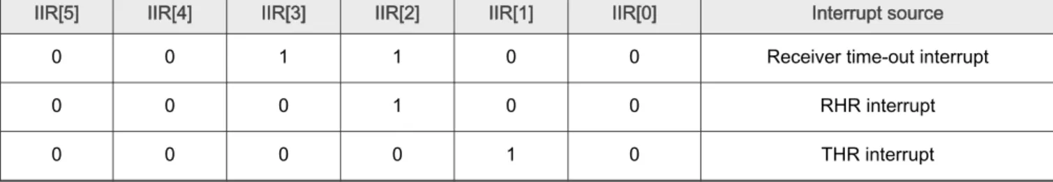
Table 3. IIR interrupt source
IIR[5] IIR[4] IIR[3] IIR[2] IIR[1] IIR[0] Interrupt source
0 0 1 1 0 0 Receiver time-out interrupt
0 0 0 1 0 0 RHR interrupt
0 0 0 0 1 0 THR interrupt
Table 4. TXLVL and RXLVL register
Register Address Read/Write mode Function
Bit Symbol Description
Transmitter Buffer Level
register (TXLVL) 0x08 Read-Only
7 — Not used, set to zero
6:0 TXLVL[6:0] Number of spaces available in TxBuffer, from 0 (0x00) to 64 (0x40)
Receiver Buffer Level
register (RXLVL) 0x09 Read-Only
7 — Not used, set to zero
6:0 RXLVL[6:0] Number of characters stored in RxBuffer, from 0 (0x00) to 64 (0x40)
5 Register-Drive operations
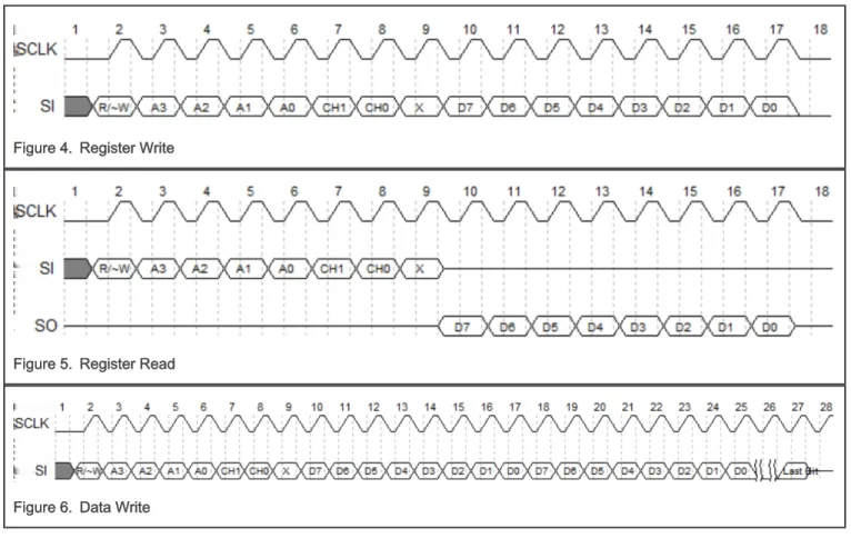
Register-drive operations of bridge can be divided into four types including register writing, register reading, data writing and data reading. As shown in Figure 4 to Figure 7, a complete register or data operation consists of two parts, one command byte and one data byte or several data bytes. Command byte is the first byte sent by the central controller. Table 5 describes the arrangement of bit field of this byte.
Figure 4. Register Write
Figure 5. Register Read
Figure 6. Data Write
Figure 7. Data Read
Table 5. Command byte bit field arrangement
Bit Symbol Description
7 R/~W(Read/~Write)
Data transfer direction
0: From central controller to USART peripheral. It is also called as downstream transfer
1: From USART peripheral to central controller. It is also called as upstream transfer
6:3 A3:A0 Register address
2:1 CH1:CH0
USART channel selection 0x00: channel 0
0x01: channel 1
0x11: channel 0 and channel 1
0 X Reserved
6 Data transmission flow
6.1 Downstream transmission flow
Downstream is defined as transmission direction which is from central controller to USART peripherals through SPI to USART bridge. Bridge contains a transmitting Buffer (Tx Buffer) of up to 64 bytes and we assume that trigger level of Tx Buffer is configured as 64 bytes. Therefore, downstream transmission contains two different cases.
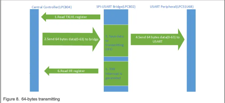
• The amount of transmitting data equal to 64 bytes
As shown in Figure 8, it is essential to read TXLVL register to ensure that Tx Buffer has enough space to hold data bytes before central controller sending 64-byte data to bridge. Then the central controller sends 64-byte-data to bridge. The bridge caches these data bytes and forwards them to specific USART channel. Later, bridge generates interrupt signal named IRQ and sends it to input pin of central controller. Once central controller detects available IRQ signal from bridge, it reads IIR register in bridge to identify interrupt source. Here, it is THR interrupt.
Figure 8. 64-bytes transmitting
• The amount of transmitting data less than 64 bytes, for example, 19 bytes
As shown in Figure 9, the transmission flow of this case is the same as the first case except for reading IIR register. There is no need to read IIR register, as bridge will not generate any interrupt in this case.
Figure 9. 19-byte transmitting
6.2 Upstream transmission flow
Upstream is defined as transmission direction which is from USART peripherals to central controller through SPI to USART bridge. Bridge contains a receiving Buffer (Rx Buffer) of up to 64 bytes and we assume that trigger level of Rx Buffer is configured as 64 bytes. Therefore, upstream transmission contains two different cases.
• The amount of receiving data equal to 64 bytes
As shown in Figure 10, , when amount of available data bytes in Rx Buffer reaches trigger level, RHR interrupt is generated by bridge and bridge sends IRQ signal to central controller. Once central controller detects IRQ signal, it will read IIR register in bridge to identify interrupt source. If interrupt source is RHR, it is necessary for central controller to read RXLVL register to obtain available data amount in Rx Buffer. Finally, central controller reads these available data bytes in Rx Buffer by sending dummy data (any data) bytes to bridge.
Figure 10. 64-byte receiving
• The amount of receiving data bytes less than 64 bytes, for example, 63 bytes
As shown in Figure 11, the transmission flow of this case is the same as the first case except for interrupt source type. Interrupt source type in this case is Rx time-out. When bridge waits to receive data from USART peripherals, if wait time exceeds the preset timeout value, the bridge considers current receiving operation to be over and Rx time-out interrupt will be generated by bridge.
Figure 11. 63-byte receiving
6.3 Upstream transmission key point
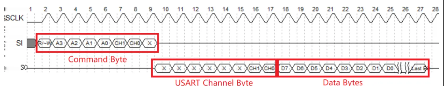
SPI is a kind of data exchange protocol. In other words, even if SPI master only wants to receive data from SPI slave, SPI master also needs to send dummy data bytes to SPI slave in order to provide serial shift clock to SPI slave. According to Figure 7, SPI master should send N+2 dummy data bytes in order to read N data bytes from SPI slave. One additional bytes aims to send command byte and the other to read USART channel number which is also the first byte from bridge.
7 Program flow
This section introduces each operation flow of SPI to USART bridge in details.
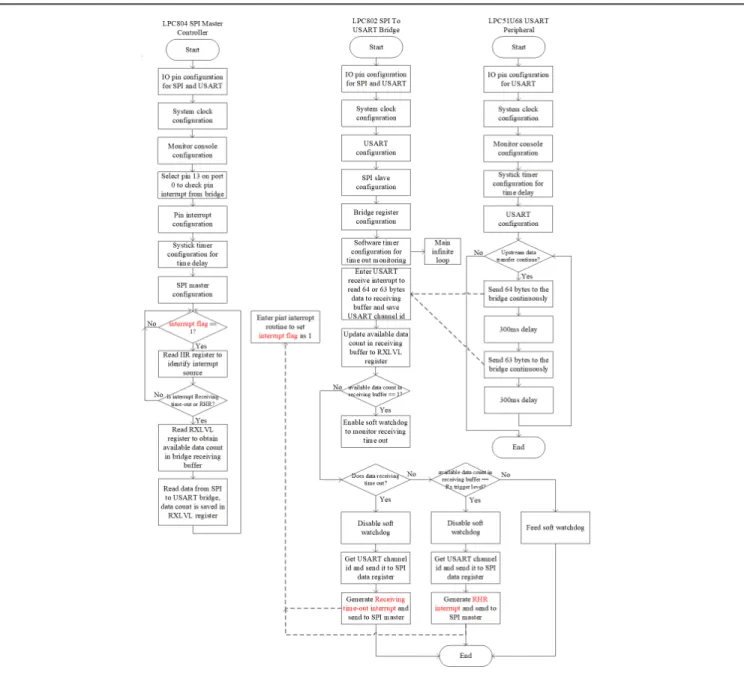
7.1 Data reading (upstream)
Figure 12 shows the program flow of data reading for SPI master from USART peripheral.
1. If bridge receives available data bytes from USART peripheral, these data bytes will be stored in receiving buffer of bridge. If available data count equals to receiving trigger level, bridge sends RHR interrupt to SPI master. Or, if the bridge does not receive data for a long time and the duration exceeds the preset timeout value, bridge will send receiving time-out interrupt to SPI master.
2. Once SPI master has checked interrupt on IRQ line from bridge, it can read IIR register to identify interrupt source type. 3. SPI master can determine available data count by reading the RXLVL register.
4. SPI master can initiate data reading command byte to bridge and then read data bytes continuously from bridge.
Figure 12. Program flow of reading data
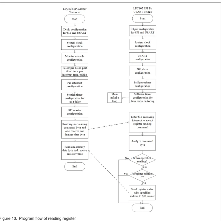
7.2 Register reading (upstream)
Figure 13 shows the program flow of register reading for SPI master from bridge. 1. SPI master sends register reading command to bridge.
2. Bridge analyzes this command to extract operation type (read/write), register address and USART channel number. 3. SPI master receives an dummy byte, any value without care. If register address is not 0, this is register reading rather
than data reading.
4. SPI master sends a dummy byte and receives register value with specified address.
Figure 13. Program flow of reading register
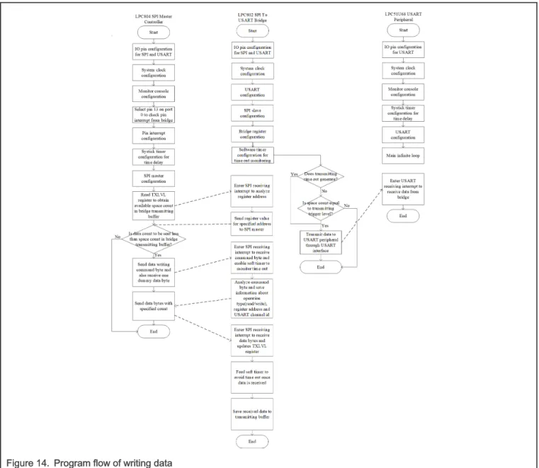
7.3 Data writing (downstream)
Figure 14 shows the program flow of data writing for SPI master to USART peripheral.
1. SPI master should read TXLVL register to get space count in transmitting buffer in bridge in order that bridge can fully receive data bytes from SPI master.
2. SPI master then sends a command byte including operation type(read/write), register address, USART channel number. 3. Bridge analyzes the byte and extracts operation type (read/write), register address, USART channel number.
Meanwhile, soft timer in bridge which is used to monitor transmitting time-out is enabled.
4. SPI master sends data bytes to bridge and bridge will receive these data bytes. Once a data byte is received, it is stored in transmitting buffer and soft timer will be fed to avoid transmitting time-out.
The bridge needs to meet two conditions to flush the transmit buffer.
• The time interval between data byte from SPI master is longer than transmitting time-out. • The data count in transmitting buffer equals to transmitting trigger level defined in TLR register.
Figure 14. Program flow of writing data
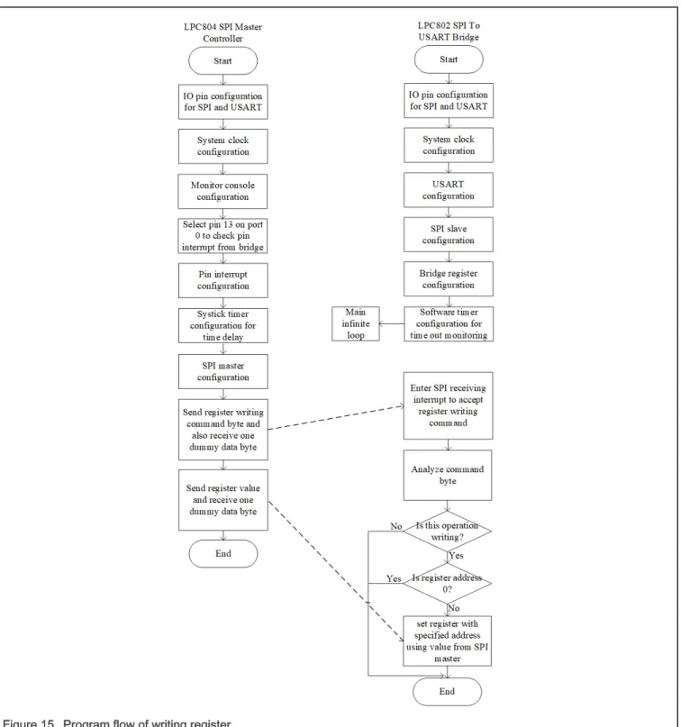
7.4 Register writing (downstream)
Figure 15 shows the program flow of register writing for SPI master to bridge. 1. SPI master transmits register writing command byte to bridge.
2. Bridge extracts control information, including operation type (read/write), register address and USART channel number from this received command byte.
3. If operation type is writing and register address is not 0, SPI master sends register value and bridge uses the value to set register with specified address.
Figure 15. Program flow of writing register
8 Demonstration setup and conclusion
8.1 Demonstration Setup
Perform the following steps to demonstrate the function of SPI to USART bridge:
1. Build three code projects corresponding to SPI master, SPI to USART bridge and USART peripherals and generate executable files.
2. Download executable files to evaluation boards, as described in Hardware configuration and interface.
3. Perform hardware connection for SPI master, SPI to USART bridge and USART peripheral, as shown in Figure 3. 4. Power up LPC802 evaluation board used as bridge and then the LPC804 and LPC51U68 evaluation boards. 5. Open two serial console terminals for SPI master and USART peripheral to observe data transmission.
6. Reset LPC804 evaluation board used as SPI master and data bytes received by USART peripheral are shown on the terminal connected to USART peripheral.
7. Reset LPC51U68 evaluation board used as USART peripheral and data bytes received by SPI master are shown on the terminal connected to SPI master.
8.2 Conclusion
As described above, data transfer consists of upstream transfer and downstream transfer. Code projects corresponding to this article provide an example to verify the function of upstream transfer and downstream transfer. Transmitting trigger level and receiving trigger level in this example are both 64 bytes.
SPI master transmits 64 data bytes from 0x00 to 0x3F and then transmits 19 bytes from 0x00 to 0x12 to USART peripheral in the downstream transfer. As shown in Figure 16, USART peripheral receives 64 data bytes from 0x00 to 0x3F and then receives 19 data bytes from 0x00 to 0x12.
USART peripheral transmits 64 data bytes from 0x00 to 0x3F and then transmits 63 bytes from 0x00 to 0x3E to SPI master in the upstream transfer. As shown in Figure 17, SPI master receives 64 data bytes from 0x00 to 0x3F and then receives 63 data bytes from 0x00 to 0x3E.
No matter whether it is upstream transfer or downstream transfer, the amount of data transferred contains two cases. • The data amount is equal to transmitting/receiving trigger level, for example, 64 bytes.
• The data amount is less than trigger level, for example, 19 bytes for downstream and 63 bytes for upstream. In either case, the data transfer is in line with expectations.
Figure 16. Downstream transmission test result
Figure 17. Upstream transmission test result
Home Page: nxp.com Web Support: nxp.com/support
to use NXP products. There are no express or implied copyright licenses granted hereunder to design or fabricate any integrated circuits based on the information in this document. NXP reserves the right to make changes without further notice to any products herein.
NXP makes no warranty, representation, or guarantee regarding the suitability of its products for any particular purpose, nor does NXP assume any liability arising out of the application or use of any product or circuit, and specifically disclaims any and all liability, including without limitation consequential or incidental damages. “Typical” parameters that may be provided in NXP data sheets and/or specifications can and do vary in different applications, and actual performance may vary over time. All operating parameters, including “typicals,” must be validated for each customer application by customer's technical experts. NXP does not convey any license under its patent rights nor the rights of others. NXP sells products pursuant to standard terms and conditions of sale, which can be found at the following address: nxp.com/SalesTermsandConditions.
While NXP has implemented advanced security features, all products may be subject to unidentified vulnerabilities. Customers are responsible for the design and operation of their applications and products to reduce the effect of these vulnerabilities on customer’s applications and products, and NXP accepts no liability for any vulnerability that is discovered. Customers should implement appropriate design and operating safeguards to minimize the risks associated with their applications and products.
NXP, the NXP logo, NXP SECURE CONNECTIONS FOR A SMARTER WORLD, COOLFLUX, EMBRACE, GREENCHIP, HITAG, ICODE, JCOP, LIFE VIBES, MIFARE, MIFARE CLASSIC, MIFARE DESFire, MIFARE PLUS, MIFARE FLEX, MANTIS, MIFARE ULTRALIGHT, MIFARE4MOBILE, MIGLO, NTAG, ROADLINK, SMARTLX, SMARTMX, STARPLUG, TOPFET, TRENCHMOS, UCODE, Freescale, the Freescale logo, AltiVec, CodeWarrior, ColdFire, ColdFire+, the Energy Efficient Solutions logo, Kinetis, Layerscape, MagniV, mobileGT, PEG, PowerQUICC, Processor Expert, QorIQ, QorIQ Qonverge, SafeAssure, the SafeAssure logo, StarCore, Symphony, VortiQa, Vybrid, Airfast, BeeKit, BeeStack, CoreNet, Flexis, MXC, Platform in a Package, QUICC Engine, Tower, TurboLink, EdgeScale, EdgeLock, eIQ, and Immersive3D are trademarks of NXP B.V. All other product or service names are the property of their respective owners. AMBA, Arm, Arm7, Arm7TDMI, Arm9, Arm11, Artisan, big.LITTLE, Cordio, CoreLink, CoreSight, Cortex, DesignStart, DynamIQ, Jazelle, Keil, Mali, Mbed, Mbed Enabled, NEON, POP, RealView, SecurCore, Socrates, Thumb, TrustZone, ULINK, ULINK2, ULINK-ME, ULINK-PLUS, ULINKpro, µVision, Versatile are trademarks or registered trademarks of Arm Limited (or its subsidiaries) in the US and/or elsewhere. The related technology may be protected by any or all of patents, copyrights, designs and trade secrets. All rights reserved. Oracle and Java are registered trademarks of Oracle and/or its affiliates. The Power Architecture and Power.org word marks and the Power and Power.org logos and related marks are trademarks and service marks licensed by Power.org.
© NXP B.V. 2020. All rights reserved. For more information, please visit: http://www.nxp.com
For sales office addresses, please send an email to: [email protected]
Date of release: November 2020 Document identifier: AN13066