International Journal of Emerging Technology and Advanced Engineering
Website: www.ijetae.com (ISSN 2250-2459, ISO 9001:2008 Certified Journal, Volume 3, Issue 4, April 2013)
697
Design of a Transceiver System at C-Band based on
Multi-Technology
Anil Kumar Pandey
SMS-EEsof R&D, Agilent Technologies, Manesar, Gurgaon-122015, India
Abstract—This paper presents design and simulation of a transceiver system for active phased array at C-Band using multi-technology based chips. Multi-technology feature is new emerging technique for complex RF and microwave systems designs where transceiver chips based on different fabrication technologies like MMIC, LTCC and microstrip are integrated on same RF board. Design and simulation of full transceiver system is very challenging because of the presence of multiple technologies in one single design. Finite Element Method (FEM) based electromagnetic solver has been used to simulate complete module. A peak module output gain 18.2 dB has been achieved at an overall module efficiency of 21%.
Keywords—MMIC, LTCC, Chip-in-package, Multi-Technology, Transceiver, Active phased Array Antenna, ADS
I. INTRODUCTION
A transceiver is a subsystem comprising both a transmitter and a receiver which are combined and share common circuitry or a single housing. When no circuitry is common between transmit and receive functions, the device is a transmitter-receiver. Technically, transceivers must combine a significant amount of the transmitter and receiver handling circuitry. Electronic countermeasures environment has become increasingly complex, forcing radar designer active phased array system using transceiver active systems.
This paper provides design and simulation of a transceiver system based on 3 different fabrication technologies. A low power 5.3 GHz phased-array transceiver that includes LNA, PA, SPDT Switch, and LTCC Low pass filter and integrated into a single chip has been presented in this paper. This design will uncover the key design techniques and challenges in implementing an
integrated, energy-efficient 5.3 GHz phased-array
transceiver using multi-technology design approach. This design combines MMIC technology and LTCC technology, developed a high level of integration of the C-band T/R module in accordance with the design requirements, the volume of 24mm x 14mm x 8mm.
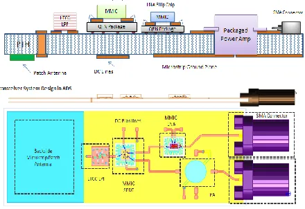
II. T/RMODULE ARCHITECTURE
System level block diagram of the T/R module is given in Fig.I. T/R module components have been designed using three different major technologies as given below.
Fig.I. Block Diagram of T/R Module
A. MMIC Technology
MMIC Single-pole-double-through (SPDT) Switch
Low Noise Amplifier (LNA) based on MMIC
non-linear process design kit (PDK)
Power Amplifier (PA)
B. LTCC Technology
LTCC Low Pass Filter : 3 pole low pass filter based
on 6 layer LTCC technology
C. QFN Packaging and Microstrip Technology
QFN Package : Standard QFN package technology
for LNA ,PA and SPDT switch packaging
Antenna : C-band microstrip patch antenna
International Journal of Emerging Technology and Advanced Engineering
Website: www.ijetae.com (ISSN 2250-2459, ISO 9001:2008 Certified Journal, Volume 3, Issue 4, April 2013)
[image:2.612.60.280.192.343.2]698
To provide isolation and minimize the possibility of oscillation the LNA is gated off in the transmit mode while the Driver Amplifier and Final Power Amplifier are off in the receive mode.Fig .II Complete Transceiver System modeled in ADS
III. T/RMODULE DESIGN AND SIMULATION
The LNA, PA and SPDT are designed using two different MMIC process design kits (PDK) having different layer stacks and material properties. Low pass filter is design using LTCC technology whereas Antenna is designed using microstrip technology. The complete transceiver circuit is realized by integrating all components in a single chip.
[image:2.612.325.564.524.653.2]Design and simulation of full transceiver system is very challenging because of the presence of multiple technologies in one single chip. FEM (Finite Element Method) solver of Agilent’s Advance Design System (ADS) has been used for complete chip realization because ADS support multi-technology based designs with different stack up in same chip. FEM simulation is carried out without active components in layout for complete system. The design is then simulated for S-Parameter in schematic with EM model along with active components. In first phase of design all individual components are modelled and optimized to meet design specification separately in ADS. Complete design flow diagram of transceiver modelling is shown in Fig III using ADS
Fig. III Flow Diagram of Complete Transceiver System modelled in ADS
A. MMIC LNA Design
International Journal of Emerging Technology and Advanced Engineering
Website: www.ijetae.com (ISSN 2250-2459, ISO 9001:2008 Certified Journal, Volume 3, Issue 4, April 2013)
[image:3.612.324.562.136.641.2]699
Fig. IV LNA design and simulation setup in ADS and simulated [image:3.612.55.279.148.238.2]S-Parameters
Fig. IV shows LNA design and simulation setup in ADS along with simulated S-Parameters from 1-8 GHz. LNA gain is 6.7 dB and Noise Figure value is 2.64 at 5GHz
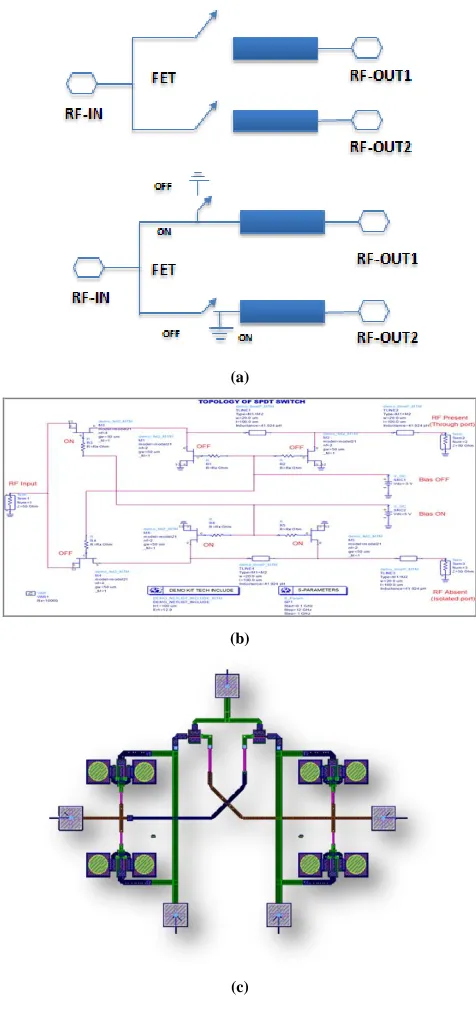
B. MMIC SPDT Switch Design
Single-Pole-Double-Throw (SPDT) switches are widely used in Transmit/Receive applications. MMIC SPDT switch has been designed using standard series-shunt configuration .MMIC design process kit contains MESFETs with non-linear models which is used as basic switching elements. SPDT switch has one input and two output arms. RF power is guided into one of the arms by switching ON the required arm and switching OFF the other arm.
Ideally, no power should be detected in the OFF arm. However, due to the parasitic and coupling effects, RF power leaks into the OFF arm. The leaked power is grounded by placing a shunt MESFET in ON state as shown in the Fig. V (a)
This reduces the power detected in the OFF arm and thus improves the isolation. SPDT switch is design first using Ideal lumped elements as shown in Fig. V (b). RF flows from Source to Drain when Gate is at 0 volt. Hence series FETs have input and output at Source and Drain respectively. Single DC bias is used to connect all ON devices and another single DC bias is used to connect all OFF devices. After verifying the basic switch action, idle components are replaced with MMIC demo-kit components in layout as shown in Fig. V (c). Fig. VI shows electromagnetic simulation model of SPDT switch inside QFN package along with S-parameter simulator result.
(a)
(b)
(c)
International Journal of Emerging Technology and Advanced Engineering
Website: www.ijetae.com (ISSN 2250-2459, ISO 9001:2008 Certified Journal, Volume 3, Issue 4, April 2013)
[image:4.612.65.266.133.356.2]700
Fig. VI Electromagnetic (EM) simulation model of SPDT switchinside QFN package along with S-parameter simulator result
C. LTCC LPF Filter
Low Temperature Co-fired Ceramic (LTCC) is a multi-layer ceramic technology, which processes the ability to embed the passive elements, such as resistors, capacitors and inductors into a ceramic interconnect package while the active elements are mounted in the top layer. In the design a 3 pole low pass filter up to 6 GHz has been designed by using spiral inductor and capacitor.
Fig. VII E-Filed over Low pass filter design based on Low Temperature Co-fired Ceramic (LTCC) technology along with
simulation data at 5 GHz.
The technology used in this example is LTCC. The basic components spiral inductor and capacitor been designed with parameterized value. Filter results as shown in Fig. VII, has been optimizing at 5GHz by varying parameters that changes value of inductor (L) and capacitor (C).
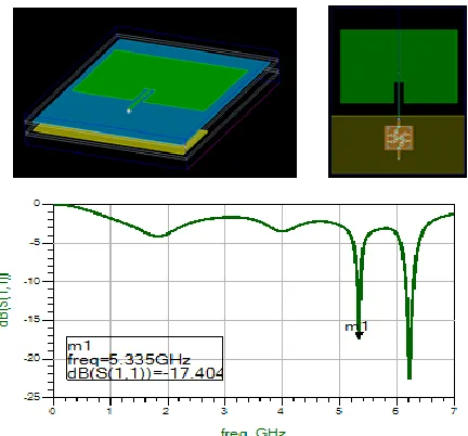
D. Microstrip Patch Antenna Design along with Via Transition
[image:4.612.335.551.443.644.2]A Microstrip antenna is created on a single Alumina substrate layers (10 mil).
[image:4.612.53.286.489.641.2]International Journal of Emerging Technology and Advanced Engineering
Website: www.ijetae.com (ISSN 2250-2459, ISO 9001:2008 Certified Journal, Volume 3, Issue 4, April 2013)
701
The operating frequency of antenna is 5.3 GHz. Antenna performance is verified along with RF board interconnects and layers transitions. Fig. VIII shows microstrip patch antenna design and simulated return loss of antenna.IV. DESIGN OF COMPLETE SYSTEM
In realization phase of complete transceiver system, first system has been simulated by placing all ideal components. Design is then optimized to get desired specification. After that all blocks has been replaced with actual modelled LNA, SPDT, LPF and microstrip antenna. In simulation model, X-parameter file has been used for Power amplifier (PA. The design is then simulated for S-Parameter. Fig. IX shows layout design and circuit simulation model of transceiver system. Layout design is solver using FEM solver then in circuit simulation EM model is used to get S-parameter data along with active components.
(a)
(b)
Fig. IX (a) Layout design and circuit simulation model of transceiver system (b) Substrate configuration of transceiver assembly
[image:5.612.344.544.284.437.2]
Fig. X S-Parameter simulation result of transceiver system
S-Parameter simulated data is shown in Fig X. Here PA is in ON state while LNA is in OFF state. Simulation gain of PA is 18.2 dB.
V. APPLICATION OF DESIGNED TRANCEIVER MODULE IN PHASED ARRAY RADAR
[image:5.612.70.258.345.669.2]International Journal of Emerging Technology and Advanced Engineering
Website: www.ijetae.com (ISSN 2250-2459, ISO 9001:2008 Certified Journal, Volume 3, Issue 4, April 2013)
702
(a)(b)
Fig. XI (a) T/R modules along with phased shifters in active phased array radar system (b) Simulation result of S-parameter data
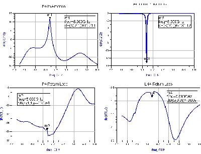
[image:6.612.59.278.128.578.2]Fig. XI (a) shows arrangement of eight T/R modules along with phase shifters and radiant linear antenna array in active phased array radar. As shown in Fig. XII, antenna array beam sequent with different phase values in feeder network. Return loss plot of linear array is below -20 dB in desired frequency band.
Fig. XII squinting of antenna beam with variation of phase
VI. RESULTS
Simulated return loss, insertion loss and phase array patterns are observed to be matching with expected results at 5.3 GHz. Detailed simulation results are given in Table I
TABLEI Results of complete system
Design name Parameters Specification
MMIC- SPDT Switch
Frequency range DC to 8 GHz
Insertion loss < 1 dB
I/O Return loss < -15 dB
Isolation > 30 dB
MMIC - LNA
Gain 6.7 dB
Noise Figure 2.64 at 5.08 GHz
Stability Factor 1.43 at 5.08 GHz
MMIC-PA Gain 18.2 dB in
LTCC- LPF Pass bandwidth Up to 5.6 GHz
I/O Return Loss < -15 dB
Microstrip
Antenna Frequency range
5-5.3 GHz ( 300 MHz )
Polarization Linear Polarization
Gain 7 dB
Transceiver
System Supply Voltage
Single Bias Supply Operation (3 V)
Overall I/O
[image:6.612.71.264.141.382.2] [image:6.612.326.563.145.274.2]International Journal of Emerging Technology and Advanced Engineering
Website: www.ijetae.com (ISSN 2250-2459, ISO 9001:2008 Certified Journal, Volume 3, Issue 4, April 2013)
703
VII. CONCLUSION
In the paper a C-Band T/R Modules was modelled and successfully simulated using various multi-technology based chips in system. Performance of complete system has been analyzed using Finite Element Method and Circuit simulation using active components in ADS. The topology used in this system improves the system performance as well as reduces chip size. The transceiver system is applied in an active phase array to demonstrate beam sequencing with variation of phase values. The simulation output shows very favorable result and shows good results for complete system. The objective of the project was successfully achieved using multi-technology design approach.
REFERENCES
[1] An AlGaN/GaN HEMT-Based MMIC Process for Advanced Transceiver, Mattias et al, IEEE 2008
[2] Andricos, Bahl, "GaAs Monolithic IC's Applied to Military [3] Radar Design" The Microwave System Designers Handbook ,
Fourth Edition 1986, pp. 335-347.
[4] A.E. Geissberger, R.A. Sadler, E.L. Griffin, I.J. Bahl and M.L. Balzan, "Refractory Self-Aligned Gate Technology for GaAs Microwave FEB and MMICs," Electron. Lett., Vol. 23, No. 29, September 1987.