FPGA BASED ADAPTIVE RESOURCE EFFICIENT ERROR
CONTROL METHODOLOGY FOR NETWORK ON CHIP
1M.DEIVAKANI, 2D.SHANTHI
1 Associate Professor, Department of Electronics and Communication Engineering
PSNA College of Engineering and Technology, Dindigul, India.
2 Professor, Department of Computer Science Engineering
PSNA College of Engineering and Technology, Dindigul, India.
E-mail: [email protected], [email protected]
ABSTRACT
This research work proposes resource efficient and secured network on chip router using error control schemes. The proposed method combines the Cipher block encryption based parallel crossbar methodologies of the NoC data link and network layers to efficiently gives error control strength in variable network topology conditions. The proposed method significantly minimizes hardware utilization when compared to other previous works. This can be achieved by implementing parallel cross bar architecture with Cipher block based ECC coding method in NoC. The proposed system uses Modelsim software for simulation purposes and Xilinx Project Navigator for synthesis purposes.
Keywords: Error Control, Cipher, Data Link, Residual Packet And Interleaving.
1. INTRODUCTION
Network-on-chip (NoC) provides a flexible communication infrastructure to be adapted for various applications with various workloads at the same time maintaining performance and simplicity. But System-on-Chip (SoC) requires a longer time to respond and to map the applications. Also SoC lacks an efficient usage of the bus systems in its design. New system has to depend on reuse of components and architectures. NoC provides a good solution for flexible products which may be reconfigurable and programmable for applications with a combined task for applications with strict time-to-market requirements. There is always a trade-off between performance and simplicity.
Generality provides hardware reuse while
performance is achieved by using application-specific structures to increase efficiency and decrease the processing time. Implanting a network instead of global wiring imparts certain advantages in performance and structure. Hence, NoC is the solution for several technological, economical and productivity problems.
In reconfigurable embedded systems, NoCs provide links which interconnect processors, memories and other intellectual property (IP) components. NoCs combine performance with
design modularity, allowing the integration of many design elements on single chip die. NoCs have been applied to SoC to avoid the complexity
of on-chip communications. On-chip
communications become more liable to transient noises, like cross-talk and external radiations. In state of art work, they introduced error minimizing methodologies to reduce the hardware errors in network router. This type of errors varies linearly in accordance with time unit. This also affects the bandwidth optimization and power consumption. In other ways, an adaptive error control techniques are used to access the network utilization efficiency. Previous works [7-10] employs ECC at the data link layer (hop-to-hop ECC), which detects errors at each link. This type of error control techniques reduces the residual error rate, but it also reduces the available utilization bandwidth and increases the power consumption.
thus, improving the energy efficiency and link reliability while maintaining performance.
2. RELATED WORKS
In [1], A. Banerjee et al proposed an energy-aware routing algorithm for NoCs. The algorithm uses a complex architecture which is the main drawback. Duan et al [2] has designed and verified a CODEC based routing schemes which avoids cross talk and other interference.
B. Fu and P. Ampadu [3] proposed a Hybrid ARQ scheme for the network interconnects. Their methodology used type2 hybrid ARQ features and
employed hamming product codes. The
experimental results showed low transmission speed and requires larger gates for a better performance. Ganguly et al [5] has designed a low power network on chip router for reliable network architecture. It also supported multiple error correction coding for this design and verification.
Kangmin Lee [6], in his paper suggested an efficient and low power NoC design to be used for low power applications. Their design made use of a hierarchical star topology based NoC for low power applications. The design used a complex architecture.
Lehtonen et al [7] has proposed error control schemes such as forward error correction methodologies for large scale network on chip routers. This paper only concentrated on error detection and correction process. In [8], S. Murali
et al presented a Dynamic Error recovery algorithm
to be used on NoCs. Their technique provided a large error rate and also supports only a less baud rate.
Xu et al [9] presented a wave-pipelined interconnect architecture for NoCs. Their results show that their design consumed high power and required more number of gates and slices.
Yu et al [10] has proposed an error controlled network router for NoCs and simulated using flexible parallel simulator. But, they focused only four ports configuration and buffer allotment for each port became variable memory unit and it consumed high power consumption.
3. PROPOSED METHODOLOGY
The proposed coding techniques merges Cipher block encryption with inter-leaving methods to adaptively adjust to the error control operation during varying noise conditions. The proposed
method lowers the residual packet error rate by implementing interleaving techniques with Cipher block based ECC Coding method in NoC. The router architecture and the encoding/decoding processes are explained in detail in the next section.
3.1. NI Architecture
The Network Interface (NI) is a part of the proposed ECC mode switching protocol. It counts the number of errors found during a time interval and requests for an ECC mode switch if necessary. The switching request architecture is shown in Figure 1. If the node is present in the Single layer (SL) state, the total number of detected
errors after a time interval beyond the End Error
Threshold makes the request. To distinguish real favourable noise conditions and the consequence of adding hop-to-hop ECC, we check logic “1” in the Error History Flit (EHF), which stores the error detected at every hop along the route. The EHF is created by the NI when it packetizes the bit stream into a packet. This EHF starts with a unique header bit to be recognized by the router and is protected with the same error protection code. The remaining elements of EHF are written at each hop as “1” for error detection and “0” for no error. Whenever a non-zero EHF is present, the value of ripple counter is incremented. The value of modular counter is incremented by 1 at each clock cycle and
this resets the ripple counter every cycles. The
number of D-flip flops needed in the modular counter and the ripple counter are equal to
and
respectively.
3.2. Router Architecture
We have designed a router which supports our proposed modified dual layer ECC and is shown in Figure 1. The designed router consists of ECC Mode Switch, Mode Propagation Counter and Error history flit (EHF) update system. A router typically has 5 input and output ports, namely, north, south, west, east and local. The information extractor obtains the destination address from the packet header flit. The arbiter provides connection between input and output ports. The arbiter makes use of NACK feedback from neighbouring routers (NACK_in) to control the first-in-first-out (FIFO) packet. In the Dual layer (DL) state and Pre-SL
state, S1=1 is transmitted to neighbouring routers to
make sure all the routers use hop-to-hop ECC. The
SL and Pre-DL states propagate S1=0 to turn off the
comes from the mode propagation counter. The
input width for that counter
is . The width of EHF is
the same as that for an uncoded flit. For a 32-bit flit
[image:3.612.94.518.79.342.2]width, the EHF can store the error history for a route length of up to 24 hops. In the network interface, the error history flit is decoded with an OR operation masked by the hop-to-hop ECC.
Figure 1. Architecture of Router for a Dual Layer-ECC
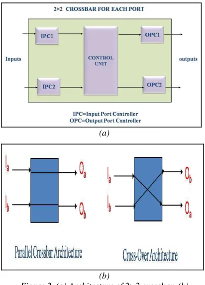
The EHF update system is explained in detail in the ECC switching algorithm section. The router consists of a crossbar switch mechanism as shown in Figure 2a. The 2×2 crossbar architecture consists of Input port controllers (IPC), output port controllers (OPC) and a control unit. Each IPC adds an Internal Header (IH) to the incoming Packet. The IH contains the forwarding route of the packet. If IH=0, then the Crossbar acts as a parallel architecture. Similarly, if IH=1, then the crossbar acts as a cross-over Crossbar. The architectures of a crossbar working in parallel and cross-over mechanism are shown in Figure 2b.
(a)
(b)
Figure 2. (a) Architecture of 2×2 crossbar, (b) Operation of a crossbar based on IH
Figure 3. The EHF update system
To avoid mode switching oscillation, only network-layer requests can change the DL state to the Pre-SL state. The time spent in the Pre-SL state is used to propagate the request through the rest of the network using the dual-layer error control. If no dual-layer mode is requested by the local node and neighbour nodes, the network enters the SL state. The dual-layer ECC mode is triggered when the total number of errors detected by any node in
cycles exceeds the error threshold. is the time
interval in which the NI counts the total number of erroneous packets. The number of error-packets is given by,
where, is the total number of bits per packet
and is the bit error rate (BER).
3.3. Dual Layer ECC Encoder
[image:3.612.317.520.273.437.2] [image:3.612.89.295.425.712.2]binary bit stream of each packet is arranged into an array where each flit is a column. There are 3 stages for an encoding process.
Stage 1: Each flit is encoded by a column
encoder (in this work, we use a systematic linear code) to generate the flit check bits (FCB).
Stage 2: The row vector is encoded by a row
encoder to produce the packet check bits (PCB) using systematic linear codes.
Stage 3: To generate the checks-on-checks
(CoC), we encode the PCB by the column encoder.
The product codes in our dual-layer ECC require an additional step to packetize the PCB and CoC into a new packet. To reduce the energy consumption for transmitting parity check bits, we transmit a coded packet first and then transmit the packet composed of PCB and CoC if a retransmission request is received.
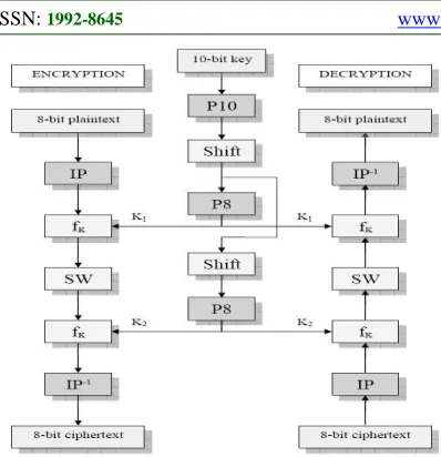
3.4. Key Generation
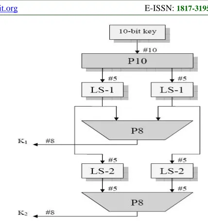
This security algorithm for router architecture uses the 10 bit length of initial key for encoding or encrypting the receiving packets in each port of the router. The two corresponding sub keys are generated by using this initial key. The generation of key and sub-keys are clearly illustrated in Figure 6. Initially, the given packet data is permuted and this permuted data is divided in to two sub blocks of same size.
[image:4.612.305.519.73.303.2]Initially the 10 bit key is permuted using permutation table P10 and this 10 bit key is divided in to 2 five bits of equal length, the first five bits are left shift by 1 and next corresponding five bits are left shift by 1.After this, the left shifted 10 bits are applied to permutation table P8 which produces first 8 bit key, called as K1.The same process is applied for remaining portions in order to get another 8 bit key length, called as K2.
Figure 4. Key Generation Flow
Input: receiving packet with data
Output: encrypted packet with data
1.Upon extracting data from receiving packet
2.If the data is available then
3.begin
4.Permute the data using P10 permutation table
5.P10 output is xor with K1
6.Switching operation is done
7.end
8.If the Switching operation is done then
9.It is xor with K2
10.end
11.perform inverse permutation
12.end
Figure 6. The Overall Key Generation Process
3.5. Dual Layer ECC Decoder
During the packet decoding procedure, initially the first received packet is decoded using routing decoder, which is available at the input port side of the router. If the received packet may have errors during transmission and these errors can be detectable and correctable within the range limit, then these packets are stored in the router internal buffer, else the received packet will be forwarded to its corresponding internal port of the router. In the mean time, if we receive the second packet from external router, these second packets can be combined or integrated with first received packet and the corresponding error patterns are decoded using such decoder.
The entire message comes in each cycle in the hop-to-hop level application of the product code. In contrast, one flit arrives at the network interface is enough to execute the first decoding step. If there are uncorrectable errors in the first transmission packet, an array of column decoders is needed to obtain the final uncoded packet. To obtain the whole packet or the check bit packet, two NI buffers are necessary. Since these buffers can be shared with the existing NI data buffers, the cost is acceptable.
4. RESULTS AND DISCUSSION
To evaluate the performance of the proposed scheme, we consider erroneous port which creates errors in other ports of the corresponding router itself. The proposed system architecture has minimal hardware utilities which provides low power consumption and reduces the routing latency in the router network on chip.
We have used Modelsim 5.5e as simulation software and Xilinx project navigator 10.1 as synthesis software to evaluate the proposed network on chip router. By analyzing the results from simulation, it shows that it produces the tolerable packet error rate and also the synthesis result shows that low hardware utilization such as 41 slices, 72 LUTs and 81mw power consumption respectively.
Table 1. Performance evaluation of power consumption and hardware utilizations
Evaluation
Parameters Banerjee [1]
Proposed methodology
Power
Consumption 92mW 81mW
Slices 75 41
LUTs 102 72
The performance evaluation parameters
considered here are Power Consumption, Slices utilization and LUTs utilization in FPGA platform. These evaluation parameters are computed for our proposed methodology based on 3s500epq208-5 FPGA package. This performance evaluation between Banerjee [1] and our approach is given in Table 1 and the same is graphically illustrated in Figure 7.
Figure 7. Graphical illustration of hardware utilizations
5. CONCLUSION
This research work proposes energy efficient and secured network on chip router using error
control schemes. The proposed method
[image:5.612.314.529.482.630.2]compared to other previous works. This can be achieved by implementing interleaving techniques with Cipher block based ECC coding method in NoC. The proposed system uses Modelsim software for simulation purposes and Xilinx Project Navigator for synthesis purposes.The proposed system consumes 81mW than the existing system and utilizes less hardware components.
REFERENCES
[1] A. Banerjee, P. T. Wolkotte, R. D. Mullins,
S. W. Moore and G. J. M. Smit 2009. An energy and performance exploration of network-on-chip architectures. IEEE Trans. Very Large Scale Integr. (VLSI) Syst. 17(3), pp. 319–329.
[2] C. Duan, V. H. C. Calle and S. P. Khatri
2009. Efficient on-chip crosstalk avoidance CODEC design. IEEE Trans. Very Large Scale Integr. (VLSI) Syst. 17(4), pp. 551– 560.
[3] B. Fu and P. Ampadu 2009. On Hamming
product codes with type-II hybrid ARQ for on-chip interconnects. IEEE Trans. Circuits Syst. I, Reg. Papers 56(9), pp. 2042–2054.
[4] B. Fu and P. Ampadu 2010. Exploiting
parity computation latency for on-chip crosstalk reduction. IEEE Trans. Circuits Syst. II, Exp. Briefs 57(5), pp. 399–403.
[5] A. Ganguly, P. P. Pande, B. Belzer and C.
Grecu 2008. Design of low power & reliable networks on chip through joint crosstalk avoidance and multiple error correction coding. J. Electron Test 24, pp. 67–81.
[6] Kangmin Lee 2006. Low-Power
Network-on-Chip for High-Performance SoC Design. IEEE Trans. Very Large Scale Integr. (VLSI) Syst., 14(2).
[7] T. Lehtonen, P. Lijieberg and J. Plosila
2007. Analysis of forward error correction methods for nanoscale networks-on-chip. In Proc. Nano-Net., pp. 1–5.
[8] S. Murali, T. Theocharides, N.
Vijaykrishnan, M. J. Irwin, L. Benini and G. De Micheli 2005. Analysis of error recovery schemes for networks on chips. IEEE Design Test Comput. 22(5), pp. 434–442.
[9] J. Xu, W. Wolf and W. Zhang 2009.
Double-data-rate, wave-pipelined
interconnect for asynchronous NoCs. IEEE Micro. 29(3), pp. 20–30.
[10] Q. Yu and P. Ampadu 2010. A flexible
parallel simulator for networks-on-chip with error control. IEEE Trans. Comput.-Aided