Technology (IJRASET)
©IJRASET: All Rights are Reserved
260
Design of Low Power Double Edge Triggered Phase
Detector for DLL Clock Generators
V. Yamuna1, Mrs. P. Meenakshi Vidya2, Dr. S. Sudha3 1,2,3
Department of ECE, Easwari Engineering College
Abstract--A DLL based double edge triggered phase detector (DET-PD) is proposed for a clock generator in low power systems. The phase detector plays a vital role in DLL clock generators. To reduce the power consumption, the phase detector is designed by combining both the edges of the clock pulse. The phase detector is designed by Truly Single Phase Clock (TSPC) delay flip flop (DFF) logic which has a faster locking speed. The operating frequency of the design ranges between 250MHz-800MHZ. The design is implemented in 180nm and 65nm CMOS process technology and the average power consumed is6.26mW and 3.92mW respectively.
Keywords--DLL, DET-PD, TSPC, DFF
I. INTRODUCTION
Low power consumption is always desired for any electronic products today. Demand for modern measurement systems in CMOS process introduce new challenges in design of low power clock generation systems. With the rapid growth in the digital systems the clock generation becomes a very important constraints. The clock generator is implemented using Delay Locked Loop(DLL) and Phase Locked Loop (PLL). PLL based clock generators can easily change the output clock frequency, but they have the problem of noise accumulation at the output due to the use of voltage controlled oscillators (VCO). The DLL overcomes this problem by using voltage controlled delay line (VCDL), and has better jitter performance. Compared to PLL, DLL is simple to design with first order system, more stable and less jitter accumulation, while PLL is a higher order system and more unstable [7]. There are three types in DLL clock generators analog, digital, mixed mode. The analog DLL clock generators are widely used because of their better jitter performance and they do not suffer from quantization error [11].
II. BLOCK DIAGRAM AND DESCRIPTION
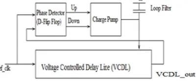
[image:2.612.212.412.536.619.2]A conventional DLL clock generator, as shown in Fig.1 has four main blocks. The voltage controlled delay line (VCDL) consist of several delay cells (inverters) connected in cascade. The delay cells can be increased to increase the frequency range of delay line. The reference clock, ref_clk drives the input to the VCDL. The output of the VCDL is given to the phase detector(PD), which determines the phase alignment error. The phase detector compares the phase difference between the ref_clk and VCDL_out signal which is the output of the VCDL line[13]. There are two main types of phase detector level sensitive phase detector and edge sensitive phase detector. The level sensitive phase detector uses XOR gate. The edge sensitive phase detector uses D flip flop.
Fig 1. Conventional DLL clock generator
III. PROPOSED ARCHITECTURE
A. Voltage Controlled Delay Line(VCDL)
Technology (IJRASET)
©IJRASET: All Rights are Reserved
261
VCDL rather than the VCO since the noise in the voltage controlled delay line does not accumulate over
[image:3.612.247.325.144.221.2]many clock cycles, hence it is preferred to be used in many cases. It also offers a faster locking time, which allows a system to reduce the wait time required before it can operate. The voltage controlled delay line (VCDL) consist of several delay cells (inverters) connected in cascade.
Fig 2. Conventional Current Starved Delay line model.
To control the delay of the inverter two extra transistors are added. This is called current starving technique. Lowering Vn and
making Vp high increases the effective drive resistance of the inverter and thus increases the delay. The inverter is designed to limit
the current sourcing and sinking capability of the inverter by adding current source and current sink in series with the upper PMOS and NMOS of the inverter. The proposed architecture of VCDL is shown in Fig 3. The control voltage Vctrl is applied to a series
[image:3.612.157.455.329.518.2]connected element. The phase difference provided by each segment of VCDL depends on the delay of each inverter.
Fig 3. VCDL Architecture
B. Phase Detector
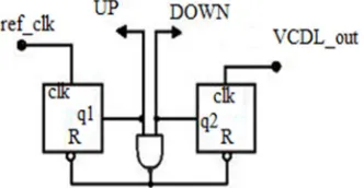
The phase detector used two D- flip flops where the reference ref_clk and VCDL signal VCDL_out which has to be compared enters as clock inputs. The UP and DOWN signals are the output of the flip flop which are given to the NAND gate. The NAND gate output is given as reset input R to both the flip flops. The block diagram of the phase detector is shown in the Fig 4. The phase detector has the probability of working in four states.
[image:3.612.224.390.611.697.2]Technology (IJRASET)
©IJRASET: All Rights are Reserved
262
C. Single Edge Triggered Phase Detector
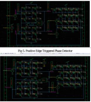
The single edge triggering phase detector (SET-PD) commonly uses flip flop design where the data is processed at either the positive or negative edges of the clock pulse. The phase detector is designed using Truly Single Phase Clock (TSPC) logic. The TSPC logic based flip flop reduces the transistor count and power consumption of the circuit.The schematic of Positive Edge Triggered (PET) phase detector is shown in Fig 5.The NOR gate is used to reset the flip flop when both UP_PET and DOWN_PET signals are at logic 0 the flip flop gets reset. If the raising edge of the ref_clk leads the VCDL_out signal then the UP output goes high. If the VCDL_out leads the ref_clk then the DOWN output goes high. If both remains low then the UP and DOWN signals will also be at logic low. TSPC logic of Negative Edge Triggered (NET) phase detector detects the phase error at the negative edge of the clock pulse. Herein NOR gate is used to reset the flip flop. The flip flop is rest when both the UP_NET and DOWN_NET pulses are at logic 0. The schematic of NET-PD is shown in Fig 6. The negative Edge Triggered (NET) requires nine transistor. The inverter and inverter delay compensation circuit are added in the negative edge triggered flip flop to avoid the gain mismatch.
[image:4.612.152.463.231.578.2]. Fig 5. Positive Edge Triggered Phase Detector
Fig 6.Negative Edge Triggered Phase Detector
D. Double Edge Triggered Phase Detector
Technology (IJRASET)
[image:5.612.144.473.77.219.2]©IJRASET: All Rights are Reserved
263
Fig.7 Double Edge Triggered Phase Detector
If the rising edge of the clock and leads the VCDL rising edge, the UP output of the phase detector goes high while the DOWN output remains low. If the VCDL signal leads the clock, UP remains low while the DOWN goes high and we can find the phase difference between VCDL and clock. In locked state, the both UP and DOWN output remains low.
IV. SIMULATION RESULT
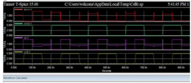
The design of VCDL,TSPC based SET-PD and DET-PD are simulated using Tanner EDA 180nm and 65nm CMOS process technology, with a supply voltage of 1.8V and 1V respectively. The frequency of operation for the design is 500MHz. Fig. 8(a) shows the VCDL output. The reference clock leads the VCDL output by 30 degree.
Fig.8(a) VCDL Output
In DET-PD the edge sensitivity problem have to be fixed so as to remove the multiple lock position while pulse merging the outputs. To overcome the dead zone problem the reset pulse gets slender in the phase locked region which provides sufficient time for the UP and DOWN signals to make the charge pump switch completely for very small phase differences. The simulation result of Positive Edge Triggered Phase Detector is shown in the Fig.8(b)
[image:5.612.146.469.362.499.2] [image:5.612.146.463.570.708.2]Technology (IJRASET)
©IJRASET: All Rights are Reserved
264
The simulation result of Negative Edge Triggered Phase Detector is shown in Fig.8(c). The NET-PD has the characteristics of the TSPC flip flop design, it has a wide capture range. It produces a large flat gain when the delay difference is twice larger than the liner gain.
.
Fig. 8(c) Negative Edge Triggered Phase Detector
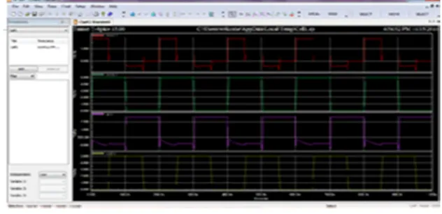
The simulation result of Double Edge Triggered Phase Detector is shown in Fig.8(d). To overcome the dead zone problem the reset pulse gets slender in the phase locked region which provides sufficient time for the UP and DOWN signals to make the charge pump switch completely for very small phase differences. The signals from the PET-PD and NET-PD are combined into one signal at the pulse merging circuit which is composed of two NAND gate.
Fig.8(d) Double Edge Triggered Phase Detector
V. PERFORMANCE ANALYSIS
Table 1 Performance Analysis of Phase Detector
VI. CONCLUSION
The clock distribution network has huge contribution in DLL design, by using the DET technique the power consumption is CMOSTech. PET-PD NET-PD DET-PD Frequency Supply
[image:6.612.150.466.120.273.2] [image:6.612.128.486.359.509.2]Technology (IJRASET)
©IJRASET: All Rights are Reserved
265
significantly reduced. The DET clock generator reduces the frequency to half while keeping the same throughput. The frequency range of analog DLL is increased by using the delay cells. The power consumption of DET phase detector is found to be 6.292mW for 180nm CMOS process and 3.919mW for 65nm CMOS process and 2.33mW for 35nm technology. The phase detector is designed to operate at a frequency of 500MHZ.The speed of the circuit operation is also increased by DET technique. The power consumed by double edge triggering technique is 32% reduced compared to conventional single edge triggering technique.
REFERENCES
[1] Sewook Hang and Kyeong Min Kim (2013), ‘A Self Calibrated DLL-Based Clock Generator for An Energy Aware ESIC Processor’, IEEE Transactions on VLSI Systems, Vol.21, No.3.
[2] Tan A. and Wei G.Y. (2012), ‘Phase Mismatch Detection and Compensation for PLL/DLL based multi-phase Clock Generator’, IEEE Solid State Circuits, Vol.37, No.11, pp.1441-1447.
[3] Kyungho Ryu and Seong Ook (2011), ‘A DLL Clock Generator for Fast Lock and Low Jitter Clock Generator’, IEEE transaction on Solid State Devices, Vol.59, No.9.
[4] Koo J. and Kim S. (2009), ‘A Low Power Programmable DLL based Clock Generator with wide range anti harmonic lock’, in Proc. 12th WSEAS International
Conference on Circuits, pp.197-201.
[5] Gang Luo and Xianjum Zeng (2008), ‘An improved Volage Controlled Delay Line for delay cells’, in Proc. Design Automation Conference, pp.131.
[6] Alvandbour A. and Mesgarzadeh B. (2008),’A 2Ghz,7-mW Digital DLL-based frequency multiplier in 90-nm CMOS’, in proc. 34th Solid State Circuits
Conference, pp.86-89.
[7] Brennnam P. and Larrson (2006), ‘A Dual Edge Triggered Phase Frequency Detector Architecture’, IEEE journal of Solid-State Circuits, Vol.38.
[8] Chulwoo Kin and Chul Hwang (2004),’A Low power Small Area and 7.28ps-Jitter PLL Based Clock generator, IEEE Journal of Solid State Cicruits, Vol.37, No.11, pp.1717-1720.
[9] Nauta .B and Vaucler C.S, (2002), ‘Low jitter clock multiplier: A comparision between PLL and DLL’, IEEE Transcation Circuits Systems, Vol.49, No.8, pp.555-566.
[10] Ahmed S.I. and Mason R.D (2001), ‘A DLL with phase detector for Fast Lock and low jitter clock generator’, IEEE Journal on Circuits and Systems, Vol.59, No.9, pp.1860-1870.
[11] Behzad Razavi (2002), ‘Design of Analog CMOS Integrated Circuits’, Tata Magraw Hill.
[12] Brennan P.V. (2001), ‘Performance of phase locked loop frequency synthesizer using acumulative phase detector’, IEEE Proc. Circuits, Devices and Systems,