B Praveenkumar1, J Thirumal Murugan2, R. Prabhakar3
1,2,3
Assistant Professor, Muthayammal Engineering College, Rasipuram, Namakkal District – 637408
Abstract— Quantum Cellular Automata (QCA) is one of the emerging nanotechnologies in which it is possible to implement reversible logic gates. QCA makes it possible to achieve high performance beyond the limits of existing CMOS technology. QCA does not have to dissipate its signal energy during transition. Further, there is no movement of electrons from one QCA cell to the other, there is no current flow. Thus, QCA has no dissipation in signal propagation. Fredkin gate can be used to design D Latch, DET flip flops and Master slave flip flops. The factors such as area, delay, power and the complexity of the design is much increased. Hence QCA technology can be implemented in order to increase the performance. In my project based on QCA computing, ripple carry adder (RCA) can be designed with high performance when compared with that of CMOS technology. In terms of testability, LFSR can be used to generate test patterns which are used as input vectors (0s and 1s) for ripple carry adder.
Keywords— QCA and Fredkin Gate INTRODUCTION
Conservative logic is a logic family that exhibits the property that there are an equal number of 1s in the outputs as in the inputs. Conservative logic can be reversible in nature or may not be reversible in nature. Reversibility is the property of circuits in which there is one to- one mapping between the inputs and the output vectors, that is for each input vector there is a unique output vector and vice-versa. Conservative logic is called reversible conservative logic when there is a one-to-one mapping between the inputs and the outputs vectors along with the property that there are equal number of 1s in the outputs as in the inputs. Conservative logic circuits are not reversible, if one-to-one mapping between the inputs and the outputs vectors is not preserved. Researchers have proved that if the computation is performed in an irreversible manner, each bit of information lost will produce KTln2 Joules of heat energy. From a thermodynamic point of view, it is also proved that kTln2 energy dissipation would not occur, if a computation is carried out in reversible way.
I. QCA TECHNOLOGY
QCA is one of the nanotechnologies in which it is possible to implement reversible logic gates [2], [3]. QCA makes it possible to achieve circuit densities and clock frequencies beyond the limits of existing CMOS technology [4], [5]. In QCA, computing logic states of 1 and 0 are represented by the position of the electrons inside the QCA cell. Thus, when the bit is flipped from 1 to 0 there is no actual discharging of the capacitor as in conventional CMOS.
Hence, QCA does not have to dissipate all its signal energy during transition. Further, propagation of the polarization from one cell to another is because of interaction of the electrons in adjacent QCA cells. As there is no movement of electrons from one QCA to another.
Fig. 1 (a) Quantum Dot and (b) QCA cell.
II. BASICS OF QCA
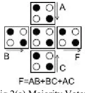
The conservative logic gates are implemented in the QCA nanotechnology, thus we are also providing the introductory material on QCA computing. A QCA cell is a coupled dot system in which four dots are at the vertices of a square. The cell has two extra electrons that occupy the diagonals within the cell due to electrostatic repulsion. Fig. 1(a) and (b) shows the four quantum dots in a QCA cell,and the implementation aof l
QCA cell, respectively. The basic QCA device is the MV or majority gates, which is represented as F = AB + BC + AC, where F is the majority of the inputs A, B, and C. Another important gate in QCA is the INV. There can be many ways of designing the QCA INV, one of which is shown in Fig.1(d). In QCA computing, signal transfer is made through wires that are of two types: 1) binary wire and 2) INV chain. The binary wire is shown in Fig. 1(e). The INV chain is shown in Fig. 1(f). In QCA, when a binary wire crosses the INV chain, there is no interaction between the two; hence, the signals in the INV chain and binary wire can pass over each other.
Fig.2(b) INVERTER Chain
III. FREDKIN GATE
The Fredkin gate is a popularly used reversible conservative logic gate, first proposed by Fredkin and Toffoli. The Fredkin gate shown in Fig. 1 can be described as a mapping (A, B, C) to (P = A, Q = A′B + AC, R = AB + A′C), where A, B, C are the inputs and P, Q, R are the outputs, respectively. Fredkin gate is reversible and conservative in nature, that is, it has unique input and output mapping and also has the same number of 1s in the outputs as in the inputs. It can be designed with D latch, master-slave flip-flops and DET flip flops for testing process.
Fig.3. Fredkin Gate
IV. DESIGN OF DLATCH
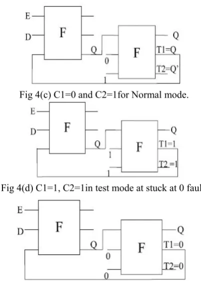
Fredkin gate can be used to design D latch in two modes. (1) Normal mode and (2) Test mode. The characteristic equation of the D latch can be written as Q+ = D · E + .E · Q. In the proposed work, enable (E)refers to the clock and is used interchangeably in place of clock. When the enable signal (clock) is 1, the value of the input D is reflected at the output that is Q+ = D. While, when E = 0 the latch maintains its previous state, that is Q+ = Q. The reversible Fredkin gate has two of its outputs working as 2:1 MUxes, thus the characteristic equation of the D latch can be mapped to the Fredkin gate (F).
Fig 4(a) Fredkin Gate with D Latch.
Fig 4(b) Control Signals C1 and C2.
Fig 4(c) C1=0 and C2=1for Normal mode.
Fig 4(d) C1=1, C2=1in test mode at stuck at 0 fault.
Fig 4(d) C1=0, C2=0in test mode at stuck at 1 fault.
1) Normal Mode: The normal mode is shown in Fig. 4(c)in which we will have C1C2 = 01 and we will have the design working as a D latch without any fan-out problem. 2) Test Mode (Disrupt the Feedback): In test mode, when
C1C2 = 00 as shown in Fig. 4(d) it will make the design testable with all 0s input vectors as output T1 will become 0 resulting in making it testable with all 0s input vectors. Thus, any stuck-at-1 fault can be detected. When C1C2 = 11 as shown in Fig. 4(e), the output T1 will become 1 and the design will become testable with all 1s input vectors for any stuck-at-0 fault. It can seen from above that C1 and C2 will DISRUPT the feedback in test mode.
V. DESIGN OF MASTER-SLAVE FLIP FLOP A negative enable reversible D latch will pass the input D to the output Q when E = 0; otherwise maintains the same state. The characteristic equation of the negative enable D latch is Q+ = D· .E +E·Q. This characteristic equation of the negative enable reversible D latch can be mapped on the second output of the Fredkin gate as shown in Fig. 5(b). The testable reversible D flip-flops has four control signals mC1,mC2, sC1, and sC2. mC1 and mC2 control the modes for the master latch, while sC1 and sC2 control the modes for the slave latch. In the normalmode, when the design is working as a master-slave flip-flop the values of the controls signals will be mC1 = 0 and mC2 = 1,sC1 = 0 and sC2 = 1 ( as similar to values of the control signals C1 and C2 earlier described for the testable D latches).
In the test mode.
signals will be mC1 = 1 mC2 = 1, sC1 = 1, and sC2 = 1. This will result in outputs mT 1 and sT 1 having a value of 1, breaking the feedback and resulting in the design testable with all 1s input vectors for any stuck-at-0 fault.
Fig 5(a). Fredkin gate-based negative enable testable D latch
Fig 5(b). Fredkin gate-based testable reversible master-slave D flip-flop.
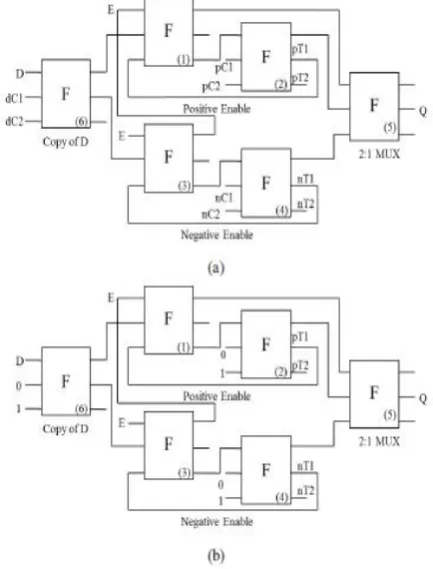
VI. DESIGN OF TESTABLE REVERSIBLE DET FLIP-FLOPS The DET flip-flop is a computing circuit that samples and stores the input data at both the edges, that is at both the rising and the falling edge of the clock. The master slave strategy is the most popular way of designing the flip flop. In the proposed work, E refers to the clock and is used interchangeably in place of clock. In the negative edge triggered master-slave flip-flop when E = 1 (the clock is high), the master latch passes the input data while the slave latch maintains the previous state. When E = 0 (the clock is low), the master latch is in the storage state while the slave latch passes the output of the master latch to its output. Thus, the flip-flop does not sample the data at both the clock levels and waits for the next rising edge of the clock to latch the data at the master latch.
In the design of testable reversible DET flip-flop, the positive enable testable reversible D latch and the negative enable testable reversible D latch are arranged in parallel. The Fredkin gates labeled as 1 and 2 forms the positive enable testable D latch, while the Fredkin gates labeled as 3
latch or the positive enable D latch) that is in the storage state (is holding its previous state) to the output Q. In the proposed design of testable reversible DET flip-flop, pC1 and pC2 are the controls signals of the testable positive enable D latch, while nC1 and nC2 are the control signals of the testable negative enable D latch. Depending on the values of the pC1, pC2, nC1, and nC2.
1) Normal Mode: The normal mode of the DET flip-flop is illustrated in Fig. 6(b) in which the pC1 = 0, pC2 = 1,nC1 = 0, and nC2 = 1. The pC1 = 0, pC2 = 1 helpin copying the output of the positive enable D latch thusavoiding the FO while the nC1 = 0 and nC2 = 1 help in copying the output of the negative enable D latch thus avoiding the FO. 2) Test Mode: There will be two test modes.
Fig. 6. Fredkin gate-based DET flip-flop. (a) Fredkin gate based DET flipflop. (b) Normal mode. (c) Test mode for
stuck-at-1 fault. (d) Test mode for stuck-at-0 fault.
VII. QCA LAYOUT OF FREDKIN GATE
QCA computing provides a promising technology to implement reversible logic gates. The layout in which the clocking zone is shown by the number next to D (D0 means clock 0 zone, D1 means clock 1 zone, and so on). It can be seen that the Fredkin gate has two level MV implementation, and it requires 6 MVs and four clocking zones for implementation. The number of clocking zones in a QCA circuit represents the delay of the circuit (delay between the inputs and the outputs). Higher the number of clocking zones, lower the operating speed of the circuit. The devices FO (F02 and F03), INV (I NV1 and I NV2), CW (CW4 and CW2) and majority voters (MJ1, MJ3, MJ4, MJ5, and MJ6) can be replaced by their fault-tolerant counterparts in the QCA layout of the Fredkin gate to have the equivalent design that gives 100% fault coverage to the two test vectors, all 1s and all 0s. In Fig. 7, the shaded boxes represent the devices that are replaced by fault-tolerant counterparts to achieve 100% fault coverage for any single missing/additional cell defects by only two test vectors, all 1s and all 0s. Thus, conservative logic based QCA circuits based on our proposed QCA layout of the Fredkin gate shown in Fig. 7 can be tested by all 0s andall 1s test vectors for presence of any single missing/additional cell defects.
Fig. 8. QCA design of MX-CQCA gate.
outputs of the MX-CQCA is: P = AB; Q = AB′+BC; R = B + C, where A, B, and C are the inputs and P, Q, R are the outputs, respectively. The MX-cqca gate requires five majority voters and 218 QCA cells with an area of 0.71 μm2. Majorit gate compared to the Fredkin gate, 11% less QCA cells and 5.4% less area.
Fig. 8. MX- CQCA gate.
Fig. 8(c). QCA layout of MX-CQCA gate.
IX. DESIGN OF RIPPLE CARRY ADDER USING QCA
The proposed system is to design Ripple carry adder (RCA) based on QCA. The layout of ripple carry adder is simple and have less interconnections. The test patterns can be generated to the inputs of the circuit in order to stimulate the inputs. Based on QCA computing, Ripple carry adder can be designed in terms to support testability.
Features CMOS QCA Technology
AREA 549 gate counts 59 gate counts
DELAY 3.509 ns 2.441 ns
POWER 32 mW 28 mW
Table 9.1 Comparison
The above table shows that the design of ripple carry adder based on QCA technology have outperform the sequential circuit implemented in classical gates in terms of area, delay, power and testability. Hence, a conventional sequential circuit needs modification in the original circuitry to provide the testing capability. Also as the complexity of a circuit is also reduced. The main advantage of the conservative reversible sequential circuits compared to the conventional sequential circuit is the need of only two test vectors to test any sequential circuit irrespective of its complexity.
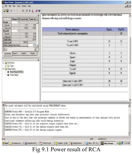
The power consumed in the design of Ripple carry adder using QCA have 28mW and that of design based on CMOS technology is 32mW. Hence the circuit also exhibits fault tolerance circuits.
Fig 9.1 Power result of RCA
X. CONCLUSION AND FUTURE WORKS This paper describes the design of the QCA circuit based on conservative logic gates outperforms the sequential circuit implemented in classical gates in terms of testability. It shows high performance than CMOS circuits. Since there is no electrons flow from one place to another, there is no power dissipation. Thus, the main advantage of the conservative reversible sequential circuits compared to the conventional sequential circuit is the need of only two test vectors to test any sequential circuit irrespective of its complexity.
Test pattern generation is the process of generating a set of input patterns to stimulate the inputs of a circuit, such that detectable faults can be sensitized and their effects can be propagated to the output. It yields high performance rather than its.
In addition, the test inputs or test vectors can be generated by LFSR (Linear Feedback Shift Register) which is used to generate test patterns. It reduces time and also provides high fault coverage, but also as an output response analyzer.
REFERENCES
[1] H. Thapliyal and N. Ranganathan, ―Reversible logic based concurrently testable latches for molecular QCA,ǁ[1].
[2] Mehdi Baradaran Tahoori and Fabrizio Lombardi, ― Testing of Quantum Dot Cellular Automata Based Designsǁ[2]. Himanshu Thapliyal, Design, Synthesis and Test of Reversible Circuits for Emerging Nanotechnologiesǁ[3].
[3] M. Hassan, A. Islam, and A. Chowdhury, Design and analysis of online testability of reversible sequential circuits,ǁ Inf. Technol., Dec. 2009, pp. 180–185.