c e-ISSN: 2348-6848, p- ISSN: 2348-795X Volume 3, Issue 01, January 2016
International Journal of Research (IJR)
Available at http://internationaljournalofresearch.orgAvailable online:http://internationaljournalofresearch.org/ P a g e | 43
ANN Based Closed loop control scheme for transformer less
DC – DC Converter
M.Babu Rao
1& S.Raj Shekar
21
M.Tech Scholar, EEE Dept , ASR College of Engineering and Technology , JUNTU-K , A.P
2Assistant Professor, EEE Dept , ASR College of Engineering and Technology , JUNTU-K , A.P
Abstract.
A bidirectional DC-DC Converter by using sliding mode controller is designed and simulated in this paper. The proposed converter employs a coupled inductor with same winding turns in primary and secondary sides. In step-up mode, to achieve high step-up voltage gain, the primary and secondary windings of the coupled inductor are charged in parallel and discharged in series. In step-down mode, to achieve high step-down voltage gain, the primary and secondary windings of the coupled inductor are charged in series and discharged in parallel. The structure of the proposed converter is very simple. Thus, the proposed converter has higher step-up and step-down voltage gains than the conventional bidirectional boos/buck converter. The operating principle and efficiency analysis are discussed in detail. Finally, a 14/42-V circuit in closed loop mode is designed and simulated to verify the performance for the automobile battery system. Keywords
Bidirectional dc-dc converter; Sliding Mode
Controller; coupled inductor
1. Introduction
Bidirectional dc-dc converters allows the transfer of power between two dc sources in either direction. These bidirectional dc-dc converters are increasingly needed in applications, such as hybrid electric vehicle energy systems, dc uninterrupted power
supplies, fuel cell hybrid power systems,
photovoltaic hybrid power systems and battery chargers. The bidirectional dc-dc flyback converters, a very simple structure [2], but the active switch suffer a high voltage stresses due to the leakage inductance of the transformer. The coupled inductor [3] type converters can provide solutions to achieve high step-up and step-down voltage gains but its circuit configuration in more complicated. The multilevel type[4] is a magnetic less converter which requires more switches to achieve high step-up and step-down voltage gains. The circuit becomes more complicated. The conventional bidirectional dc-dc boost/buck converter which is simple in structure
and easy to control as shown inFig.1.
VL VH
L1
S1
S2
Fig.1.Conventional Bidirectional DC-DC Converter
However, the step-up and step-down voltage gains of the conventional bidirectional dc-dc converter are low due the effect of power switches. To achieve the high step-up and step-down voltage gains, a novel bidirectional dc-dc converter is proposed as shown in Fig.2
The proposed bidirectional dc-dc converter employs a coupled inductor with same windings turns in the primary and secondary sides.
VL
L1
L2 S1
S2
S3
Coupled Inductor
VH
Fig.2.Proposed Converter
The organisation of the paper is as follows, Sec-2 describes the operation of the proposed converter. In Sec-3, the voltage mode control of the proposed converter is described. In Sec-4, MATLAB/Simulink models and Results are discussed. Sec-5 concludes the dynamic response of the proposed converter in open loop and closed loop mode.
2.
Operation
2.1.
Step-Up Mode
c e-ISSN: 2348-6848, p- ISSN: 2348-795X Volume 3, Issue 01, January 2016
International Journal of Research (IJR)
Available at http://internationaljournalofresearch.orgThe voltages across the coupled inductor can be expressed as follows
𝑣𝐿1= 𝐿1
𝑑𝑖𝐿1 𝑑𝑡 + 𝑀 𝑑𝑖𝐿2 𝑑𝑡 = 𝐿 𝑑𝑖𝐿1 𝑑𝑡 + 𝑘𝐿 𝑑𝑖𝐿2
𝑑𝑡 (1)
𝑣𝐿2= 𝑀
𝑑𝑖𝐿1
𝑑𝑡 + 𝐿2
𝑑𝑖𝐿2
𝑑𝑡 = 𝑘𝐿
𝑑𝑖𝐿1
𝑑𝑡 + 𝐿
𝑑𝑖𝐿2
𝑑𝑡 (2)
Mode 1: The Fig.3(b). Shows the current flow path of the
proposed converter in step-up mode, Mode 1 operation. During this mode, the switches S1 and S2 are turned on and
S3 is turned off. The primary and secondary windings of
the coupled inductor are in parallel.
Thus voltages across inductors L1 and L2 is obtained
as
𝑣𝐿1= 𝑣𝐿2= 𝑉𝐿 (3)
Substituting Eq’s(1&2) in Eq(3), we get
𝑑𝑖𝐿1(𝑡)
𝑑𝑡 =
𝑑𝑖𝐿2(𝑡)
𝑑𝑡 =
𝑉𝐿
1 + 𝑘 𝐿, 𝑡0≤ 𝑡 ≤ 𝑡1 (4)
Mode 2: During this mode of operation, the switch S1 and
S2 are turned off and switch S3 of the proposed converter
is turned on. The Fig.3(c). Shows the current flow path of the proposed converter in step-up mode, Mode 2
operation. Thus the inductor currents through the primary and secondary windings of the coupled inductor and the voltages across the inductor L1 and L2 are obtained as
follows
𝑖𝐿1= 𝑖𝐿2 5
𝑣𝐿1+ 𝑣𝐿2= 𝑉𝐿− 𝑉𝐻 6
Substituting Eq’s(1,2 and 5) in Eq(6), we get
𝑑𝑖𝐿1(𝑡)
𝑑𝑡 =
𝑑𝑖𝐿2(𝑡)
𝑑𝑡 =
𝑉𝐿− 𝑉𝐻
2 1 + 𝑘 𝐿, 𝑡1≤ 𝑡 ≤ 𝑡2 (7) By using the state-space averaging method, the following equation is derived from Eq(4) and Eq(7)
𝐷𝑉𝐿
1 + 𝑘 𝐿+
1 − 𝐷 (𝑉𝐿− 𝑉𝐻)
2 1 + 𝑘 𝐿 = 0 (8) Simplifying (8), the voltage gain is given as
𝐺(𝑠𝑡𝑒𝑝 −𝑢𝑝 )=
𝑉𝐻
𝑉𝐿
=1 + 𝐷
1 − 𝐷 (9)
2.2.
Step-down Mode
The proposed converter in step-down mode, the primary and secondary windings of the coupled are operated in series charge and parallel discharge. The proposed converter in step-down mode is shown in Fig.4(a). The Pulse width modulation technique is used to control the switch S3 Meanwhile; the switches S1and S2
are the synchronous rectifiers.
Mode 1: During this mode of operation, the switches S1
and S2 are turned off and switch S3 is turned on. Fig.4(b).
shows the current flow path of the proposed converter in step-down Mode 1 operation. The current flowing through the inductors and the voltages across the primary and secondary windings of the coupled inductor are expressed as follows
𝑖𝐿1= 𝑖𝐿2 10
𝑣𝐿1+ 𝑣𝐿2= 𝑉𝐻− 𝑉𝐿 11
On substituting Eq’s (1,2&10) in Eq(11),we get
𝑑𝑖𝐿1 𝑡
𝑑𝑡 =
𝑑𝑖𝐿2 𝑡
𝑑𝑡 =
𝑉𝐻− 𝑉𝐿
2 1 + 𝑘 𝐿, 𝑡0≤ 𝑡 ≤ 𝑡1 12
Mode 2: The current flow path of the proposed converter
in step-down Mode 2 operation is shown in Fig.4(c). During this, mode of operation, switches S1 and S2 are
turned on and switch S3 is turned off. Therefore the
voltages across the inductors L1 and L2 are expressed as
𝑣𝐿1= 𝑣𝐿2= −𝑉𝐿 13
On substituting Eq(1),(2) in Eq(13), we get
𝑑𝑖𝐿1 𝑡
𝑑𝑡 =
𝑑𝑖𝐿2 𝑡
𝑑𝑡 = −
𝑉𝐿
1 + 𝑘 𝐿, 𝑡1≤ 𝑡 ≤ 𝑡2 14
The following equation is obtained from Eq’s(12&14), by using the state space averaging method
𝐷(𝑉𝐻− 𝑉𝐿)
2 1 + 𝑘 𝐿 −
(1 − 𝐷)𝑉𝐿
1 + 𝑘 𝐿 = 0 (15) Finally, on simplifying Eq(15), the voltage gain of the proposed converter in step-down mode operation is obtained as
𝐺(𝑠𝑡𝑒𝑝 −𝑑𝑜𝑤𝑛 )=
𝑉𝐿
𝑉𝐻
= 𝐷
2 − 𝐷 (16)
VL
L1 S2
S3
CH RH
+ vL1 -+ + vDS2
--vDS3 +
iL
iL1 iS2
iS1
+
iS3 icH I0
iL2
+ VH
- VL
L1 S2
S3
CH RH VL
L1
L2
S1
S2
S3
c e-ISSN: 2348-6848, p- ISSN: 2348-795X Volume 3, Issue 01, January 2016
International Journal of Research (IJR)
Available at http://internationaljournalofresearch.orgAvailable online:http://internationaljournalofresearch.org/ P a g e | 45
RL
L1
L2
S1
S2
S3
-vL1
+
+ vDS1
-+ vDS2
--vDS3 +
iS2
iS1
-vL2
+
iS3
iL2
CL
iL1 I0 icL
+ VL
-VH
iLL
RL L1
L2
S1
S2
S3
CL +
- V
H R
L L1
L2 S1
S2
S3
CL +
-VH
c e-ISSN: 2348-6848, p- ISSN: 2348-795X Volume 3, Issue 01, January 2016
International Journal of Research (IJR)
Available at http://internationaljournalofresearch.org3.
Voltage Mode Control of the
proposed converter
PWM
Vref +
-DC-DC Converter
Vo
Vo
Sliding Mode Controller
Fig.5.Basic Block diagram of the proposed converter.
The block diagram of the proposed converter by using Sliding mode controller is shown in Fig.5.
4.
MATLAB/Simulink Models and
Results
The design parameters, MATLAB/Simulink Models of the proposed converter and the MATLAB program for calculating the efficiency of the proposed converter are discussed in this section
4.1 Design Parameters
The design parameters of the proposed converter are shown in Table.1.
Table .1. Tabular form indicating the Design Parameters of the proposed converter.
Mode of Operation
Step-up
Step-down
Input
14v
42v
Output
42v
14v
Frequency
50KHz
50KHz
Power
200W
200W
Inductance
15.5µH
15.5µH
Capacitance
330 µF
330µF4.2 MATLAB/Simulink Models and Results
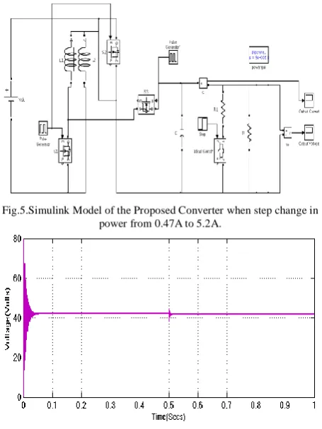
Fig.5.Simulink Model of the Proposed Converter when step change in power from 0.47A to 5.2A.
Fig.8.Output Voltage Waveform of the proposed converter when a step change in load from 0.47A to 5.2A at t=0.5sec.
c e-ISSN: 2348-6848, p- ISSN: 2348-795X Volume 3, Issue 01, January 2016
International Journal of Research (IJR)
Available at http://internationaljournalofresearch.orgAvailable online:http://internationaljournalofresearch.org/ P a g e | 47 The MATLAB/Simulink model of the proposed
converter in open loop is shown in Fig.7. The output voltage shown in Fig.8, undergoes a transient voltage deviation of 8.3% at t=0.5 sec is shown in Fig.9. The output current waveform is shown in Fig.10.
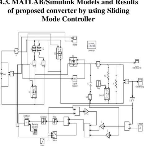
4.3. MATLAB/Simulink Models and Results
of proposed converter by using Sliding
Mode Controller
Fig.11.Simulink Model of the Proposed Converter when a step change in load from 0.47A to 5.2A at t=0.5sec
Fig.12.Output Voltage Waveform of the proposed converter when a step change in load from 0.47A to 5.2A at t=0.5sec.
Fig.13.Transient Voltage Deviation (Output Voltage waveform enlarged) of the proposed converter at t=0.5sec.
Fig.14.Output Current Waveform of the proposed converter when a step change in load from 0.47A to 5.2A at t=0.5sec. The MATLAB/Simulink model of the proposed converter by using Sliding Mode controller is shown in Fig.11.
The output voltage shown in Fig.12, undergoes a transient
voltage deviation of 0% at t=0.5 sec is shown in Fig.13. The output current waveform is shown in Fig.14.
4.4
Table for Comparison
The comparison of the proposed converter in open loop and closed loop mode is tabulated in Table.2.
Mode Voltage
Dip
Settling Time (at t=0.5 secs)
Open loop 8.33% 0.015secs
Sliding Mode
Controller 0% 0 secs
c e-ISSN: 2348-6848, p- ISSN: 2348-795X Volume 3, Issue 01, January 2016
International Journal of Research (IJR)
Available at http://internationaljournalofresearch.orgFig.15.efficiency plot of the proposed and conventional
converter in step-up mode.
Fig.16.efficiency plot of the proposed and conventional converter in step-down mode.
6.Conclusion
A bidirectional dc-dc converter is designed and simulated in this paper. The dynamic performance of the proposed converter by using Sliding Mode controller is better than the open loop performance and also the proposed converter achieves the higher up and step-down voltage gains than conventional converter. The efficiency of the proposed converter in step-up mode is 99.2% and in step-down mode is 88.5% at full load condition.
References
[1]. L.S.YANG, T.J.LIANG, “Analysis and implementation of a novel bidirectional dc-dc converter.” IEEE Trans. Ind. Electron., vol.59, no.1, pp.422-434, Jan.2012.
[2]. f. Z. Peng, f. Zhang, and z. Qian, “A magnetic-less dc–dc converter for dual-voltage automotive systems,” IEEE Trans. Ind. Appl., vol. 39, no. 2,pp. 511– 518, Mar./Apr. 2003.
[3]. T. BHATTACHARYA, V. S. GIRI, K. MATHEW, and L. UMANAND, “Multiphase bidirectional flyback converter topology for hybrid electric vehicles,”IEEE Trans. Ind. Electron., vol. 56, no. 1, pp. 78–84, Jan. 2009.
[4]. R. J. WAI and R. Y. DUAN, “High-efficiency
voltage diversity,” IEEE Trans. Power Electron.,vol. 22, no. 5, pp. 1986–1996, Sep. 2007.
[6]. L. Schuch, C. Rech, H. L. Hey, H. A. Grundling, H. Pinheiro, and J. R. Pinheiro, “Analysis and design of a new high-efficiency bidirectional
integrated ZVT PWM converter for DC-bus and battery-bank interface,” IEEE Trans. Ind. Appl., vol. 42, no. 5, pp. 1321 1332, Sep./Oct. 2006.
[7]. G. Ma, W. Qu, G. Yu, Y. Liu, N. Liang, and W. Li, “A zero-voltageswitching bidirectional dc–dc converter with state analysis and softswitching-oriented design consideration,” IEEE Trans. Ind. Electron., vol. 56, no. 6, pp. 2174–2184, Jun. 2009.
[8]. Z. Liao and X. Ruan, “A novel power management control strategy for stand-alone photovoltaic power system,” in Proc. IEEE IPEMC, 2009, pp. 445– 449.
[9]. T. Qian and B. Lehman, “Coupled input-series and output-parallel dual interleaved flyback converter for high input voltage application,” IEEE Trans. Power