Dual-Band Reconfigurable Graphene-Based Patch Antenna
in Terahertz Band: Design, Analysis and Modeling
Using WCIP Method
Aymen Hlali*, Zied Houaneb, and Hassen Zairi
Abstract—The resonant frequency of an antenna plays a crucial role in the design of a reconfigurable antenna. In this article, we have developed a dual-band reconfigurable terahertz patch antenna by using graphene. The simulation results demonstrate that the designed structure can provide excellent properties in terms of dual wide-band performance, frequency-reconfiguration by applying different voltages on the graphene. These initial results are particularly promising for various applications in the THz regime. Furthermore, we have investigated the effect of the additional parameter such as temperature and relaxation time. The modeling is done by using a new equation of the Wave Concept Iterative Process (WCIP) method, and the validation is achieved by comparison with CST simulator. Here, we propose to develop a new efficient and flexible numerical tool for graphene modeling.
1. INTRODUCTION
THz band is a portion of electromagnetic spectrum including frequencies in the range of 0.1 THz to 10 THz [1]. This band becomes extremely attractive due to essential properties such as the ability to pass through different materials with various levels of attenuation [2] and the abundance of bandwidth [3]. It has been used in numerous fields including spectroscopy, high-resolution radar, imaging and, more recently, wireless communications [4–7].
However, the THz regime is one of the ongoing challenges facing electronic and photonic materials and device engineering [8]. The solution to these developments is the exploration of the characteristics of new materials and devices at high frequencies. In search of efficient solutions to these problems, graphene appears as an excellent candidate for the implementation of new devices. Due to its unique properties at terahertz (THz) frequencies [9], graphene has attracted huge interests since it was successfully exfoliated in 2004 [10]. One of the most interesting properties of this material is its ability to support transverse magnetic surface plasmonic modes with unique properties. Specifically, graphene plasmons possess more confinement, low loss and good tunability via chemical or electrostatic gating at THz frequencies [11, 12]. It should be noted that, after the groundbreaking impact of graphene, the scientific community is actively exploring other two-dimensional semiconductors “beyond graphene”, such as phosphorene and Bi2Se3 [13, 14], for their promising applications capabilities, ranging from
nanoelectronics, nanophotonics and nanomedicine [15, 16].
A reconfigurable antenna is designed in a manner that it is possible to manually or automatically change its resonant frequency, operational bandwidth, radiation pattern. This is most commonly done with electromechanical systems (MEMS or NEMS) [17, 18], electrical RF switches [19, 20], diode-based technology such as the P-type Insulator N-type diode (PIN diode) [21, 22], varactors [23], or tunable
Received 1 August 2018, Accepted 2 October 2018, Scheduled 16 October 2018
* Corresponding author: Aymen Hlali ([email protected]).
materials [24], via applying a mechanical, electrical, magnetic, light or thermal bias [25]. The most significant merit is that the properties of graphene-based antennas can be easily controlled using electric field effect in the THz frequency. Thus, the tunability of graphene has been widely used for small reconfigurable devices in the terahertz regime.
The paper is structured as follows. Section 2 will introduce the conductivity of graphene and a brief introduction to the wave concept iterative process method, including the development of the new operator diffraction of the graphene in the spatial domain. Then, Section 4 will define the proposed antenna designs. Afterwards, the simulation results are presented and discussed in Section 5. Finally, Section 6 will finish the paper with key conclusions.
2. FORMULATION
2.1. Modeling of Graphene
Graphene is modeled as a sheet conductor whose surface conductivity consists of two terms intraband conductivity and interband conductivity [26]. However, in the Terahertz-frequency band, the first term dominates the value of total conductivity whereas the second term has no significant effect on the overall surface conductivity within this band [27]. Hence, the conductivity of graphene can be expressed by using the only intraband term, which can be evaluated as
σintra=−j e
2K BT π2(ω−j2Γ)
μc KBT
+ 2 ln
e−KBTµc + 1
(1)
and the interband conductivity is
σinter −j e2
4πln
2|μc| −(ω−j2Γ)
2|μc|+ (ω−j2Γ)
(2)
where KB is the Boltzmann constant, the reduced Planck’s constant, e the electron charge, ω the
angular frequency, Γ the scattering rate, T the temperature, and μc the chemical potential. The
intraband conductivity is a complex quantity that can be expressed byσ =σr+jσi, where σr and σi
are respectively the real and imaginary parts of the conductivity.
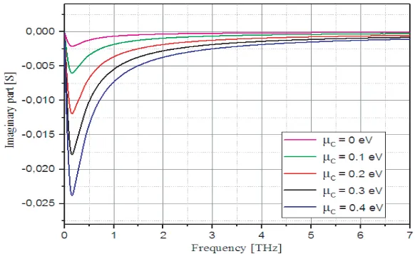
The variations of the real and imaginary parts of the intraband conductivity versus frequency for several different chemical potentials μc for 0 to 0.4 eV with T = 300 K and τ = 10−13s are shown in
Figs. 1 and 2.
From these two figures, we can see the effect of changing chemical potential on the conductivity; it depends on the carrier density, which can be controlled by a bias voltage. The relation between the
Figure 2. Imaginary part of graphene’s conductivity.
Figure 3. The relationship between bias voltage and chemical potential.
bias voltage and chemical potential in graphene obtained from Eq. (3) is shown in Fig. 3 [28].
Vg = eμc 2h
π2V2 fε0εr
(3)
where Vg is the applied voltage on graphene, h the thickness of the substrate, εr the substrate
permittivity, and Vf the Fermi velocity in graphene.
We observe that the potential chemical increases with an increase in bias voltage, hence the increase of the conductivity. Therefore, reconfigurable characteristics can be obtained.
2.2. Modeling of Graphene in the WCIP Method
Analysis of planar structures with our electromagnetic method called wave concept iterative method WCIP has been described in detail in various articles [29, 30]. Therefore, a brief overview of the WCIP method is presented here. It is based on the Wave Concept, which is introduced by writing the incident and reflected waves as a function of the transverse electric and magnetic fields. It leads to the following set of equations
Ai =
1 2√Z0i
Ei+Z0iJi
Bi =
1 2√Z0i
Ei−Z0iJi
(5)
whereiindicates medium 1 or 2 corresponding to a given interface. Z0i is the characteristic impedance
of the same medium i, and Ji the surface current density vector is given as
Ji =Hi×ni (6)
withni being the normal vector to the interface. Thus, the tangential electric and magnetic fields can
be calculated from
Ei =
Z0i
Ai+Bi
(7)
Ji =
1
√ Z0i
Ai−Bi
(8)
After process convergence the scatring matrixSij can be obtained by the following equation
[S] = 1−[Y]
1 + [Y] (9)
where [Y] is the matrix admittance.
In order to implement the model of graphene sheet in the WCIP method, the boundary conditions at the sheet can be represented as [27]
n×H1 −H2 = Js (10a)
= σ E (10b)
where n denotes the unit vector normal to the graphene sheet; H1 and H2 are the magnetic fields at two sides of the sheet; Js is the surface current density; E is the electric field. Generally, modeling by
the WCIP method consists of converting the magnetic field H by the current density J, and we can write
n×H1 −H2 =J1 +J2 (11)
The electric field may be written as
E=E1 =E2 (12)
By replacing Equations (8) and (9) in Equation (7), we obtain the following equations
J1+J2 = σ E1 (13)
J1+J2 = σ E2 (14)
In terms of waves and after a mathematical resolution, these equations are finalized at
B1 B2 = S11 S12 S21 S22 A1 A2 (15)
whereSij are defined by
S11 = Z02−Z01−σZ02Z01
Z02+Z01+σZ02Z01 (16)
S12 = 2Z02
√ Z01 √
Z02(Z02+Z01+σZ02Z01) (17)
S21 = 2Z01
√ Z02 √
Z02(Z02+Z01+σZ02Z01) (18)
S22 = −Z02−Z01+σZ02Z01
The interface in which the circuit is defined is divided into small sub-domains, and the interface contains four sub-domains (dielectric, metal, graphene and source). By using the boundary condition in each region [31, 32], it is possible to define the overall diffraction operator, which binds the incident waves to the reflected waves in the spatial domain:
Γ = ΓG+ Γm+ Γd+ Γs=
Γ11 Γ12
Γ21 Γ22
(20)
where ΓG,Γm,Γd and Γs are respectively the graphene, metal, dielectric and source domain diffraction
operators.
with Γij is expressed by
Γ11 =
−Hm+Z02−Z01−σZ02Z01 Z02+Z01+σZ02Z01Hg+
1−n2 1 +n2Hd+
−1 +n1−n2 1 +n1+n2 Hs
Γ12 =
2Z02√Z01
√
Z02(Z02+Z01+σZ02Z01)Hg+ 2n
1 +n2Hd+
2m
1 +n1+n2Hs
Γ21 =
2Z01√Z02
√
Z02(Z02+Z01+σZ02Z01)Hg+ 2n
1 +n2Hd+
2m
1 +n1+n2Hs
Γ22 =
−Hm−Z02−Z01
+σZ02Z01
Z02+Z01+σZ02Z01Hg− 1−n2 1 +n2Hd+
−1−n1+n2 1 +n1+n2 Hs
wheren= Z01 Z02,m=
Z0 √
Z01Z02,n1 = Z0
Z01 and n2 = Z0 Z02.
3. DESIGN OF THE PROPOSED ANTENNA
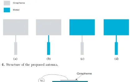
In this paper, the design of the dual-band reconfigurable graphene antenna started with a comparative investigation of no-doped graphene and metal. Figures 4(a), (b), (c) and (d) show the front view of the proposed antenna, with four different configurations, chosen for their simplicity and ease of fabrication.
(a) (b) (c) (d)
Figure 4. Structure of the proposed antenna.
All the antennas consist of a conducting patch and a feeding line and are printed on a Duroid dielectric substrate with relative permittivity 2.2 and height 3µm.
Figure 5 shows the 3D view of our proposed dual-band reconfigurable graphene antenna controlled by the bias voltage. Table 1 gives the optimized dimensional parameters of the antenna.
Table 1. Parameters of the proposed antenna.
Parameters Value (µm) Substrate length and width 103×97
Substrate thickness 3 Substrate dielectric constant (Duroid,r) 2.2
Side length and width of square patch 23.33×28.79 Length of feed 23.33
Width of feed 4.54
Length ofλ/4 transformer 14.48 Width of λ/4 transformer 1.51
4. NUMERICAL RESULTS AND DISCUSSIONS
In this section, we perform a detailed discussion about the response of the dual-band reconfigurable graphene antenna. The formulation developed in Section 2 is implemented in FORTRAN code. The main target is to prove the applicability of the formulation of graphene in WCIP in the THz range. In fact, we present different numerical results for the four configurations shown in the previous section.
4.1. Comparative Investigation of No-Doped Graphene and Metal
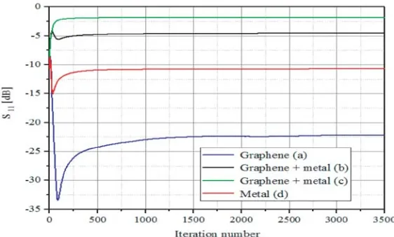
In order to compare the performance of no-doped graphene and metal for the proposed nano-patch antenna in the terahertz region, we simulated the structures presented in the previous section. For this purpose, we started with the convergence study and boundary conditions. The convergence of the iterative process is examined for the four configurations. Figure 6 shows the variation of the return loss as a function of the number of iterations at the resonant frequencies.
(a) (b)
(c) (d)
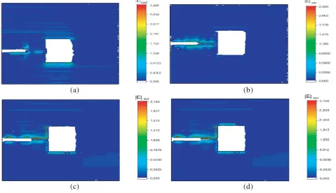
Figure 7. Distribution of the current density of the interface for the four configurations. (a) Graphene. (b) Graphene + metal. (c) Graphene + metal. (d) Metal.
(a) (b)
(c) (d)
We find that the convergence of the graphene-based antenna (a) is obtained from 1500 iterations and 700 iterations for the other structures. Figures 7 and 8 illustrate the distribution of currents and fields for each structure.
According to these figures, we notice that the electric field and current density satisfy the boundary conditions, since the density of the current is defined only on the graphene and metal, and zero on the dielectric. The electric field is zero on graphene and metal, and different from zero on the dielectric.
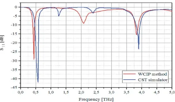
To validate the results obtained by the formulation of the graphene developed by the WCIP method, a comparison with the results obtained by the CST simulator was realized. Figure 9 shows the graph that compares the return loss of the no-doped graphene-based antenna (a) obtained through the WCIP method and CST simulator.
Figure 9. Comparative curves of the return loss S11 of no-doped graphene-based antenna (a) versus frequency.
We notice that the simulated result obtained by WCIP is very close to that obtained by the CST simulator. This also validates the formulation of the graphene developed by the WCIP method.
Figure 10 illustrates the variation of the reflection coefficient for the four studied configurations mentioned in the previous section.
Figure 10. Performance comparison of the return loss versus frequency for the four configurations.
is enhanced drastically compared to the metal-based antenna in terms of the reflection coefficient. In this case, the return loss is reduced from−10 to −24 dB.
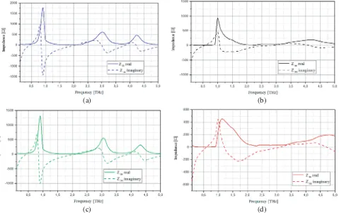
According to Figures 10 and 11, graphene-based antenna (a) showed better adaptation. For this, we continue our study with this antenna.
(a) (b)
(c) (d)
Figure 11. Real and imaginary parts of input impedance for the four configurations. (a) Graphene. (b) Graphene + metal. (c) Graphene + metal. (d) Metal.
4.2. Performance Analysis of Reconfigurable Graphene Antenna
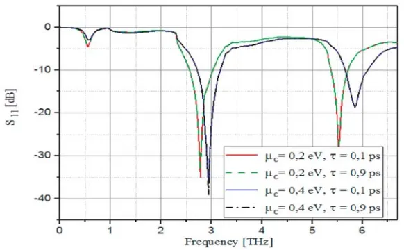
Here, the performance of the graphene-based antenna (a) was evaluated. The simulation results obtained for return loss characteristics over the considered 0.1–0.4 eV range of chemical potential are shown in Figure 12. Here the temperature is assumed 300 K, and the relaxation time is selected as 0.1 ps.
It can be seen that it exhibits two resonant frequency bands over the whole frequency range, namely 2.5–2.95 and 5.06–5.84 THz. It is exciting to note that the return loss decreases by increasing the chemical potential in the first resonance band and the reverse in the second band. The resonant frequency shift observed is irregular and somewhat linear.
Figure 13 shows the values obtained for voltage standing wave ratio (VSWR) for its potential chemical values from 0.1 to 0.4 eV at their respective resonating frequencies.
Figure 13. VSWR versus frequency for different chemical potential.
Another parameter is the relaxation time of the graphene, which is studied in Figure 14, and the temperature effect in graphene is considered at Figure 15.
Figure 14. Return loss versus frequency for various graphene with various relaxation times.
Figure 15. Return loss versus frequency for various graphene with various temperatures.
(a) (b)
(c) (d)
Figure 16. Return loss versus frequency for various substrates materials. (a) μc = 0.1. (b) μc = 0.2.
(c)μc = 0.3. (d)μc = 0.4.
relaxation time does not have any effect on this antenna.
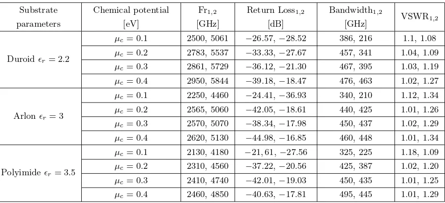
Next, the performance comparison of the proposed graphene-based dual-band antenna for various substrate materials is investigated. It can be observed in Figure 16 that return loss values for different materials reach their peak values below −10 dB at resonating frequency around 2500–2950 and 4460– 5844 GHz for all the selected substrates. The best conditions are achieved for Arlon with 0.4 eV for the chemical potential with return loss reaching the maximum value of −44.98 dB.
For various substrate materials, the bandwidth achieved is in the range of 210–495 GHz at different resonant frequencies as depicted in Table 2. It can be seen that the maximum bandwidth of 495 GHz is obtained for the Polyimide substrate withμc = 0.4 eV.
Table 2. Performance comparison of the proposed antenna for various substrate materials.
Substrate parameters
Chemical potential [eV]
Fr1,2
[GHz]
Return Loss1,2
[dB]
Bandwidth1,2
[GHz] VSWR1,2
Duroidr= 2.2
μc= 0.1 2500, 5061 −26.57,−28.52 386, 216 1.1, 1.08 μc= 0.2 2783, 5537 −33.33,−27.67 457, 341 1.04, 1.09 μc= 0.3 2861, 5729 −36.12,−21.30 467, 395 1.03, 1.19
μc= 0.4 2950, 5844 −39.18,−18.47 476, 463 1.02, 1.27
Arlonr= 3
μc= 0.1 2250, 4460 −24.41,−36.93 340, 210 1.12, 1.34 μc= 0.2 2565, 5060 −42.05,−18.61 440, 425 1.01, 1.26 μc= 0.3 2570, 5070 −38.34,−17.98 450, 437 1.02, 1.29
μc= 0.4 2620, 5130 −44.98,−16.85 460, 448 1.01, 1.34
Polyimider= 3.5
μc= 0.1 2130, 4180 −21,61,−27.56 325, 225 1.18, 1.09 μc= 0.2 2310, 4560 −37.22,−20.56 425, 387 1.02, 1.20
μc= 0.3 2410, 4740 −42.01,−19.03 450, 435 1.01, 1.25 μc= 0.4 2460, 4850 −40.63,−17.81 495, 445 1.01, 1.29
A second important observation is that as the value of potential chemical increases, the bandwidth should increase.
5. CONCLUSION
In this paper we analyze the performance of using graphene in frequency reconfigurable antennas in the THz regime for medical and imaging applications. The results clearly show the antenna can be tuned via changing the chemical potential. So, the bias electric field is a significant factor for the reconfigurable THz antenna. Furthermore, we have investigated the effect of additional parameters such as temperature and relaxation time. Fabrication of the prototype and experimental study of the proposed structure are needed in the future to validate our intended results.
REFERENCES
1. Kyungho, H., T. K. Nguyen, I. Park, and H. Han, “Terahertz Yagi-Uda antenna for high input resistance,”J. Infrared Millim. Terahertz Waves, Vol. 31, 441–451, 2010.
2. Kazemi, A. H. and A. Mokhtari, “Graphene-based patch antenna tunable in the three atmospheric windows,” Inter. J. Light Electron Opt., Vol. 142, 475–482, 2017.
3. Ramezan, A. S. and B. Z. Ferdows, “Metamaterial Fabry-Perot cavity implementation for gain and bandwidth enhancement of THz dipole antenna,”Inter. J. Light Electron Opt., Vol. 127, 5181–5185, 2016.
5. Mir, M. S. and A. S. Ramazan, “Antenna gain enhancement by using metamaterial radome at THz band with reconfigurable characteristics based on graphene load,”J. Opt. Quant. Elec., Vol. 221, 1–13, 2017.
6. Alexander, I. M., Y. Bin, M. G. Stephen, W. Michael, and S. D. Robert, “Terahertz spectroscopy: A powerful new tool for the chemical sciences?,”Chem. Soc. Rev., Vol. 41, 2072–2082, 2012. 7. Nikita, V. Ch., E. F. Maxim, P. Sergey, et al., “Wide-aperture aspherical lens for high-resolution
terahertz imaging,” Rev. Sci. Instrum., Vol. 88, 1–6, 2017.
8. Dhillon, S. S., M. S. Vitiello, E. H. Linfield, A. G. Davies, M. C. Hoffmann, et al., “The 2017 terahertz science and technology roadmap,” J. Phy. D: Appl. Phy., Vol. 50, No. 4, 1064–1076, 2017.
9. Novoselov, K. S., V. I. Colombo, P. R. Gellert, M. G. Schwab, and K. Kim, “A roadmap for graphene,” Nature, Vol. 490, No. 7419, 192–200, 2012.
10. Novoselov, K. S., A. K. Geim, S. V. Morozov, D. Jiang, Y. Zhang, S. V. Dubonos, I. V. Grigorieva, and A. A. Firsov, “Electric field effect in atomically thin carbon films,”Science, Vol. 306, No. 10, 666–669, 2004.
11. Antonio P. and Ch. Gennaro, “Plasmon modes in graphene: Status and prospect,” The Royal Society of Chemistry, Vol. 6, 10927–10940, 2014.
12. Tamagnone, M., J. S. Gymez-Dıaz, J. R. Mosig, and J. Perruisseau-Carrier, “Reconfigurable terahertz plasmonic antenna concept using a graphene stack,”Appl. Phys. Lett., Vol. 101, 214101– 214104, 2012.
13. Leonardo, V., H. Jin, C. Dominique, P. Antonio, K. Wojciech, and S. V. Miriam, “Efficient terahertz detection in black-phosphorus nano-transistors with selective and controllable plasma-wave, bolometric and thermoelectric response,”Scientific Reports, Vol. 6, 1–23, 2016.
14. Leonardo, V., C. Dominique, P. Antonio, K. Konstantin, A. Ziya, B. Mahammad, et al., “Plasma-wave terahertz detection mediated by topological insulators surface states,” Nano Letters, Vol. 16, 1–18, 2016.
15. Tang, W., A. Politano, C. Guo, W. Guo, C. Liu, and L. Wang, X. Chen, and W. Lu, “Ultrasensitive room-temperature terahertz direct detection based on a bismuth selenide topological insulator,” Adv. Funct. Mater., 1–9, 2018.
16. Amit, A., S. V. Miriam, V. Leonardo, C. Anna, and P. Antonio, “Plasmonics with two-dimensional semiconductors: From basic research to technological applications,”Nanoscale, Vol. 10, 1–11, 2018. 17. Jung, C. W., M. J. Lee, G. P. Li, and F. D. Flaviis, “Re-configurable scan-beam single-arm spiral antenna integrated with RFMEMS switches,” IEEE Trans. Antennas Propag., Vol. 54, No. 2, 455–463, 2006.
18. Cetiner, B. A., G. R. Crusats, L. Jofre, and N. Biyikli, “RF MEMS integrated frequency reconfigurable annular slot antenna,” Journal Title Abbreviation, Vol. 58, No. 3, 626–632, 2010. 19. Pringle, L. N., et al., “A reconfigurable aperture antenna based on switched links between
electrically small metallic patches,” IEEE Trans. Antennas Propag., Vol. 52, No. 6, 1434–1445, 2004.
20. Aboufoul, T., A. Alomainy, and C. Parini, “Reconfiguring UWB monopole antenna for cognitive radio applications using GaAs FET switches,” IEEE Antennas Wireless Propag. Lett., Vol. 11, 392–394, 2012.
21. Peroulis, D., K. Sarabandi, and L. P. B. Katehi, “Design of reconfigurable slot antennas,” IEEE Trans. Antennas Propag., Vol. 53, No. 2, 645–654, 2005.
22. Lee, S. W. and Y. Sung, “Compact frequency reconfigurable antenna for lte/wwan mobile handset applications,” IEEE Trans. Antennas Propag., Vol. 63, No. 10, 4572–4577, 2015.
23. Khidre, A., F. Yang, and A. Z. Elsherbeni, “A patch antenna with a varactor-loaded slot for reconfigurable dual-band operation,” IEEE Trans. Antennas Propag., Vol. 63, No. 2, 755–760, 2015.
25. Haupt, R. L. and M. Lanagan, “Re-configurable antennas,”IEEE Antennas Propag. Mag., Vol. 55, No. 1, 49–61, 2013.
26. Hanson, G. W., “Dyadic Green’s functions and guided surface waves for a surface conductivity model of graphene,”J. Ap. Phys., Vol. 103, 064302–064302, 2008.
27. Cao, Y. S., L. J. Jiang, and A. E. Ruehli, “An equivalent circuit model for graphene-based terahertz antenna using the PEEC method,”IEEE Trans. Antennas Prop., Vol. 64, 1385–1393, 2016. 28. Gatte, M. T., P. J. Soh, H. A. Rahim, R. B. Ahmad, and F. Malek, “The performance
improvement of THz antenna via modeling and characterization of doped graphene,” Progress In Electromagnetics Research M, Vol. 49, 21–31, 2016.
29. Houaneb, Z., H. Zairi, A. Gharsallah, and H. Baudrand, “A new wave concept iterative method in cylindrical coordinates for modeling of circular planar circuits,”Eighth Inter. Multi-Conference on Systems, Signals Devices, 1–7, 2011.
30. Hajlaoui, A., H. Trabelsi, and H. Baudrand, “Periodic planar multilayered substrates analysis using wave concept iterative process,”J. Elec. Analy. Appl., Vol. 3, 118–128, 2012.
31. Zairi, H., A. Gharsallah, A. Gharbi, and H. Baudrand, “Analysis of planar circuits using a multigrid iterative method,”IEE Proc. Micro., Antennas and Prop., Vol. 153, 109–162, 2006.