338
Area Efficient Implementation of Reversible Encoder and
Decoder
N.Venkatesh M.Tech1,M.V.Sowjanya,N.Harish2,N.Uma Maheswararao3,K.Madhupavani4 Assistant Professor, Dept of ECE, Tirumala Engineering College, Jonnalagadda, Narasaraopet, A.P, IndiaB.Tech
scholar, Dept of ECE, Tirumala Engineering college, Jonnalagadda, Narasaraopet, A.P, India
Abstract:Encoders and Decoders are one of the most extreme basic circuits used in combinational logic. In today’s world reversible encoder and decoder is one of the vital parts of any framework having numerous applications in PCs, portable, calculators and so on. Reversible logic has turned out to be one of the ongoing rising examination interests adding to the field of low power dissipation circuit plan in the previous couple of years. In this paper we proposed 3*6 reversible encoder and decoder circuits. We have executed reversible arithmetic logic unit dependent on reversible encoder and decoder. The issue of limiting the quantity of garbage outputs is a vital issue in reversible rationale structure. Reversible encoder and decoder comprise of various gates. Reversible Logic possesses its applications in different fields which incorporate Quantum Computing, Optical Computing, Nanotechnology, Computer Graphics, low power VLSI Etc., Reversible logic is picking up its very own significance lately to a great extent because of its property of low power utilization. The Circuit has been executed and reenacted utilizing Xilinx programming.
KEY WORDS: Cost, Reversible Gates, Garbage Outputs, Number of Gates, Encoder and decoder.
1. INTRODUCTION
In the present days, reversibility has turned out to be fundamental piece of computerized world to make advanced circuits progressively proficient. Reversible logic plays out all tasks in an invertible way that denotes a promising new bearing. As contrast and conventional rationale, all calculations can be returned. Power scattering and warmth age is a significant issue for the present PC chips. Landaulet demonstrated that utilizing conventional (irreversible) rationale entryways dependably lead to vitality scattering. Though, reversibility in Computing implies that no data about the computational states can ever be lost, so it very well may be recuperated at any before stage by processing in reverse the outcomes.
Most conventional PCs lose data during the time spent calculation. Consider the straightforward two information Boolean AND entryway: Observing a yield of 0 does not give enough data to recognize the information mix that offered ascend to the yield. Truth be told, any of three distinctive information mixes (00, 01, 10) would constrain the yield of the AND entryway to 0. In registering the consistent AND of two bits, a conventional AND door would dispose of that info data. The main characteristically consistently reversible conventional natives incorporate the wire and inverter. The finishes of Landauer and Bennett demonstrate that a vitality loss of kTln2 joules as warmth unavoidably goes with each piece of data disposed of amid calculation, and that a totally reversible PC is hypothetically conceivable. Just by playing out the calculation in a
sensibly reversible way would energy be able to scattering fall underneath kTln2 joules per bit per cycle. . Power emergency is a fundamental issue in this day and age. As of late, the developing business sector of electronic frameworks experiences control scattering and warmth evacuation issue. Assuming increasingly more power is scattered, framework ends up over warmed which decreases the existence time of the electronic framework.
Fundamentally, in encoder bit is moved into the uttermost left stage at each data and the bits in advance existing in the development registers are moved one position to right. In the wake of applying the modulo-2 activity relating yields are gotten. This system of continues until the arrival of data at the information of encoder. The choice of relationship between the development registers and adders delineates the traits of code. By fluctuating the affiliations, characteristics of the code can be changed. To depict an encoder, set of "n" affiliation vectors are required. These affiliations portray which move register is joined with m adders. A "1" in the position demonstrates that, move register is joined with the viper and a "0" in given position will show that not a singular affiliation exits between the stage and the snake.
339 Decoders can have an empower line, which works as
pursues: If empower is actuated, at that point the decoder's yields carry on of course, that is, precisely one is enacted whenever. On the off chance that the empower input isn't dynamic, at that point every one of the 2 n yields of the decoder are deactivated. In this work we manage reversible decoders without empower input.
The need of microelectronic circuits with low power dispersal prompts the usage of reversible logic circuit. Bennett demonstrated that the balanced mapping between the information sources and yields of reversible circuit definitely lessens the power utilization and warmth dispersal of a circuit. Today security in advanced figuring and interchanges is of prime significance and accordingly cryptographic conventions assume a noteworthy job. There are four noteworthy structure parameters of reversible circuits. First is the quantum cost which is the quantity of fundamental quantum gate like Controlled NOT, Controlled V+ and so forth in the reversible circuit. Second is the quantum profundity likewise called quantum delay. Third is the quantity of auxiliary data sources or ancilla inputs which are consistent information sources which are utilized to keep up the reversibility of the gadget. Fourth is the quantity of trash yields for example yield signals which are not utilized as contributions to different gates and are just there to look after reversibility. .
2. LITERATURE REVIEW
Gopi Chand Naguboina et al., reversible logic is the rising field for inquire about in display period. The point of this paper is to acknowledge distinctive sorts of combinational circuits like snake, full-subtractor, multiplexer and comparator utilizing reversible decoder circuit with least quantum cost. Reversible decoder is planned utilizing Fredkin doors with least Quantum cost. There are numerous reversible rationale doors like Fredkin Gate, Feynman Gate, Double Feynman Gate, Peres Gate, Seynman Gate and some more. Reversible rationale is characterized as the rationale in which the number yield lines are equivalent to the quantity of information lines i.e., the n-info and kyield Boolean capacity F(X1, X2, X3,… ,Xn) (alluded to as (n, k) work) is said to be reversible if and just on the off chance that (I) n is equivalent to k and (ii) each information design is mapped particularly to yield design. The entryway must keep running forward and in reverse that is the information sources can likewise be recovered from yields. At the point when the gadget complies with these two conditions then the second law of thermo-flow ensures that it disseminates no warmth. Fan-out and Feed-back are not permitted in Logical Reversibility. Reversible
Logic possesses its applications in different fields which incorporate Quantum Computing, Optical Computing, Nanotechnology, Computer Graphics, low power VLSI Etc., Reversible logic is picking up its own particular significance lately to a great extent because of its property of low power utilization. The near investigation regarding refuse yields, Quantum Cost, quantities of doors are likewise introduced. The Circuit has been actualized and reproduced utilizing Xilinx programming.
340 significantly enhances over a traditional outline of
decoder can be developed to enhance the waste yield comes at the cost of a somewhat higher quantum cost. Arvind Kumar et al. inferred that the 2 to 4 decoder utilizes fredkin gates. Since every one of the three fredkin gate reversible in nature consequently having less power dissemination. Configuration can be reached out up to n to 2n decoder. A 4 to 16 decoder has been outlined utilizations 15 consistent sources of info and 4 junk yields. This work is very viable as far as execution with three fredkin gate; add up to defer will be more which thus prompts more power dissemination guarantees that this plan isn't a compelling methodology.
3. REVERSIBLE LOGIC GATES
An gate is said to be reversible if the (Boolean) work it figures is Objective i.e., there is balanced and onto correspondence between its information and yield. A gate is reversible if there is a particular yield task for each unmistakable information. In this manner, a reversible entryway's sources of info can be remarkably decided from its yields. The information vector can be exceptionally decided from the yield vector and the other way around. A fundamental
condition is that the circuit has a similar number of info and yield wires.. A necessary condition is that the circuit has the same number of input and output wires. Binary reversible gates compute the logic values 0 and 1. Basically, the stored program architecture is given by John Von Neumann, where the each bit is estimated by the process of heat dissipation per Computation. Heat dissipation is obtained by the Destruction of bits as per Landauer Principle. Bannett proposed a Turing machine for loss-less computation by making it reversible. After Toffoli proposed reversible logic gates the development of reversible gates and circuits started. After this various number of gates have been proposed. Two categories are described namely basic gates and generalized gates.
A gate which is reversible can realize a reversible function; computation done by a gate is reversible in nature that means for a gate g the inverse
transformation is implemented as gate g-1. Some of the basic gates are given below:
A) Not Gate: the below figure (1) shows the block diagram of NOT gate. Here A is input and A1 is output.
Fig.1: NOT Gate (a) Block Diagram (b) Schematic Representation Table.1 Truth Table of NOT Gate
B) Feynman Gate was given by Richard Feynman; it is known as a reversible gate of 2×2. Feynman gate can perform negation operation but in controlled way and this reversible gate is also called Controlled NOT Gate. If two line are A and B, the first line A is known as CONTROL
341 Fig.2: Feynman Gate (a) Block Diagram (b) Schematic Representation
Table.2 Truth Table of Feynman Gate
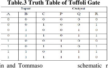
C) Toffoli Gate: is a new gate. This gate is known as 3×3 gate and can be generalized up to n×n size. As per definition target line flips when all
[image:4.612.218.395.393.504.2]control lines are set. The block diagram and schematic representation of 3×3 toffoli gate is exhibited in below figure (3).
Fig. 3: 3×3 Toffoli Gate (a) Block Diagram (b) Schematic Representation
Table.3 Truth Table of Toffoli Gate
D) Fredkin Gate: Edward Fredkin and Tommaso Toffoli proposed a new gate called 3×3 Fredkin Gate which is further generalized up to n lines. Figure.4 exhibits the block diagram and
[image:4.612.209.406.559.694.2]schematic representation of new gate called Fredkin gate. If C=0 3×3 Fredkin gate will swaps the values of A and B.
342
4. DESIGN OF PROPOSED ENCODER
AND DECODER
The Reversible Logic includes the utilization of Reversible Gates comprises of a similar number of data sources and yields i.e., there ought to be coordinated mapping between information vectors and yield vectors. What's more, they can be made to run reverse way moreover. Certain restrictions are to be viewed as when structuring circuits dependent on reversible rationale (I) Fan out isn't allowed in reversible logic gate and (ii) Feedback is likewise not allowed in reversible rationale. In Reversible logic gate utilizing yields can acquire full information of sources info. Reversible rationale monitors data. Some cost measurements like Garbage yields, Number of gates, Quantum cost, consistent sources of info are utilized to appraise the execution of reversible circuits. Waste yields are the additional yields which help to make information sources and
yields level with so as to look after reversibility. They are kept alone without playing out any activities.
Number of gates check is definitely not a decent measurement since progressively number of gates can be taken together to shape another gate. Quantum Cost is the quantity of rudimentary expected to execute the gate. It is only the quantity of reversible gate (1×1 or 2×2) required to develop the circuit. Deferral is one of the essential cost measurements. A Reversible circuit configuration can be demonstrated as a grouping of discrete time cuts and profundity is summation of all out time cuts. In Digital Electronics the paired decoder is a combinational rationale circuit that changes over the twofold number an incentive to the related yield design. Different proposition are given to plan of combinational and successive circuits in the experiencing research
.
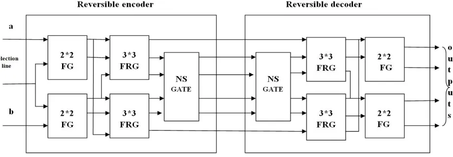
Fig. 5: 3*6 REVERSIBLE ENCODER AND DECODER The below figure (5) shows the design of proposed
reversible encoder and decoder. In this we use Feynman gate, fredkin gate and NS gate to perform
[image:5.612.77.537.491.651.2]343 reverse” as a reversible encoder. Simply reflecting
the proposed reversible decoder design horizontally as shown in figure (5) which yields a gate that can reversibly implement a 3-to-6 encoder. This reversible 3-to-6 encoder design assumes–like traditional encoders–that exactly one of its four inputs will have an input value of logical 1 at any time. When functioning this way as a reversible 3-to-6 encoder, it has zero constant inputs and two garbage outputs. Because the reversible 3-to-6 encoder design consists entirely of the same hardware as the reversible 3-to-6 decoder simply in a different (reflected) configuration, it has quantum cost and quantum delay eight, equal to the decoder configuration. To the best of our knowledge this is the first binary reversible 3-to-6 encoder. The rows are also permuted in order to group the possible input combinations.
In general, reversibly implementing a logical OR function is very costly, especially as the number of inputs increases. The Feynman gate currently can generate the two-input function most cheaply. Therefore the existing designs incur a quantum cost at least four times the quantum cost of a single reversible AND function. Our proposed reversible 3-to-6 decoder design reversibly generates all necessary AND functions using a Fredkin gate and minimal supplementary logic. Our new proposed unit has quantum cost, two constant inputs, and zero garbage outputs. The input variable columns are permuted in order to group the constant inputs a and b, and show the outputs of the reversible decoder with inputs A and selection line. The highlighted rows show the required decoding functionality. So compared to other encoders and decoders, reversible encoder and decoder provides effective results.
5. CONCLUSION
In this paper we designed 3*6 reversible encoder and decoder. These circuits are designed for minimum quantum cost and minimum garbage outputs. This method of designing combinational circuits helps to implement many digital circuits with better performance for minimum quantum cost. The proposed designs are being implemented using VHDL and simulated results are obtained using Xilinx software. The proposed designs are compared with the previous designs. However, further research interest for designing combinational circuits enables to put in force many virtual circuits with higher overall performance for minimum quantum cost.
REFERENCES
[1] R. Landauer, “Irreversibility and heat generation in the computational process,”
IBM Journal of Research and Development, 5, pp. 183-191, 1961.
[2] C. Bennett, “Logical reversibility of computation,” IBM Journal of Research and Development, pp. 525-532, November 1973. [3] E. Fredkin, T. Toffoli, “Conservative logic,” International Journal of Theoretical Physics, vol. 21, no. 3–4, pp. 219–253, 1982. [4] T. Toffoli, “Reversible computing,” Tech
memo MIT/LCS/TM-151, MIT Lab for Computer Science, 1980.
[5] A. Peres, “Reversible logic and quantum computers,” Physical Review A, vol. 32, no. 6, pp. 3266–3276, Dec. 1985.
[6] M. Mohammadi and M. Eshghi, “On figures of merit in reversible and quantum logic designs,” Quantum Information Processing, 8(4):297– 318, Aug. 2009.
[7] H. Thapliyal and N. Ranganathan, "Design of reversible latches optimized for quantum cost, delay and garbage outputs," VLSI Design, 23rd International Conference on, vol., no., pp.235-240, 3-7 Jan. 2010.
[8] Smolin, D. Divincenzo, “Five two-bit quantum gates are sufficient to implement the quantum Fredkin gate,” Physical Review A, vol. 53, no. 4, pp.2855-2856, April 1996. [9] W. Hung, X. Song, G. Yang, J. Yang, M.
Perkowski, "Optimal synthesis of multiple output Boolean functions using a set of quantum gates by symbolic reachability analysis,” Computer-Aided Design of Integrated Circuits and Systems, IEEE Transactions on, vol.25, no.9, pp.1652-1663, Sept. 2006.
[10] K. Buch , “Low power fault tolerant state machine design using reversible logic gates,” Military and Aerospace Programmable Logic Devices Conference, September 2008.
[11] M. Khan, M. Perkowski, “Quantum realization of ternary encoder and decoder,” Proceedings of the 7th International Symposium on Representations and Methodology of Future Computing Technologies, September 2005.