POWER-EFFICIENT CURRENT-MODE
ANALOG CIRCUITS FOR HIGHLY
INTEGRATED ULTRA LOW POWER
WIRELESS TRANSCEIVERS
PhD. dissertation prepared to obtain the Doctor degree
By
Fermín Esparza Alfaro
Supervisor:
Prof. Antonio J. López Martín
Pamplona, September 2014
Electrical and Electronic Engineering DepartmentUNIVERSIDAD PÚBLICA DE NAVARRA
DEPARTAMENTO DE INGENIERÍA ELÉCTRICA Y ELECTRÓNICA
Tesis doctoral: Power-Efficient Current-Mode Analog Circuits for Highly Integrated Ultra Low Power Wireless Transceivers
Autor: D. Fermín Esparza Alfaro Directores: Prof. Antonio J. López Martín Tribunal nombrado para juzgar la Tesis Doctoral citada: Presidente:
Vocal: Secretario:
Acuerda otorgar la calificación de
vii
ABSTRACT
In this thesis, current-mode low-voltage and low-power techniques have been applied to implement novel analog circuits for zero-IF receiver backend design, focusing on amplification, filtering and detection stages.The structure of the thesis follows a bottom-up scheme: basic techniques at device level for low voltage low power operation are proposed in the first place, followed by novel circuit topologies at cell level, and finally the achievement of new designs at system level.
At device level the main contribution of this work is the employment of Floating-Gate (FG) and Quasi-Floating-Gate (QFG) transistors in order to reduce the power consumption. New current-mode basic topologies are proposed at cell level: current mirrors and current conveyors. Different topologies for low-power or high performance operation are shown, being these circuits the base for the system level designs.
At system level, novel current-mode amplification, filtering and detection stages using the former mentioned basic cells are proposed. The presented current-mode filter makes use of companding techniques to achieve high dynamic range and very low power consumption with for a very wide tuning range. The amplification stage avoids gain bandwidth product achieving a constant bandwidth for different gain configurations using a non-linear active feedback network, which also makes possible to tune the bandwidth. Finally, the proposed current zero-crossing detector represents a very power efficient mixed signal detector for phase modulations. All these designs contribute to the design of very low power compact Zero-IF wireless receivers.
The proposed circuits have been fabricated using a 0.5μm double-poly n-well CMOS technology, and the corresponding measurement results are provided and analyzed to validate their operation. On top of that, theoretical analysis has been done to fully explore the potential of the resulting circuits and systems in the scenario of low-power low-voltage applications.
viii
TABLE OF CONTENTS
List of acronyms
xi
Parameter glossary
xiii
Chapter
1
Introduction
1
1.1
Motivation
1 1.1.1 Why Analog? 2 1.1.2 Why Low-Voltage? 8 1.1.3 Why Low-Power? 3 1.1.4 Why Current-Mode? 31.2
Short distance LP wireless communication standards
51.3
Low-Power Receivers
61.3.1 Low-IF receiver 7
1.3.2 Zero-IF receiver 8
1.4
Objectives
101.5
Structure of the thesis
11Bibliography of the Chapter
12Chapter
2
Low-power and low-voltage design techniques
21
2.1
Floating and Quasi-Floating Gate MOS Transistors
22 2.1.1 The Floating Gate MOS Transistor 22 2.1.2 The Quasi-Floating Gate MOS Transistor 242.2
Low quiescent current techniques
252.1.1 Class AB operation 25
2.3
Low voltage techniques
262.3.1 Dynamic Cascode biasing 26
2.3.2 Sub threshold operation: weak inversion 27
2.3.3 Companding 29
2.4
Conclusions
32Bibliography of the Chapter
33Chapter
3
Basic class AB current-mode blocks
39
ix
3.1.1 Class A and class AB current mirrors 40 3.1.2 Class AB current mirror with dynamic cascode biasing 42 3.1.3 High Performance Class AB Current Mirrors 50 3.1.4 Current mirror applications 54
3.2
Current Conveyors
553.2.1 The class AB second generation current conveyor 57 3.2.2 Second generation current conveyor applications 57
3.3
Conclusions
58Bibliography of the Chapter
59Chapter
4
Ultra low power tunable current mode filter design
63
4.1
Hyperbolic sin filter synthesis
644.1.1 Frey method 65
4.1.2 Tsividis method 66
4.1.3 Comparison of the two methods 69
4.2
Hyperbolic sin filter implementation
694.2.1 The Geometric Mean Splitter 70 4.2.2 The current multiplier / divider 72
4.2.3 The sinh transconductor 73
4.3
Hyperbolic sin channel selection filter design
744.4
Measurement results
774.5
Conclusions
79Bibliography of the Chapter
80Chapter
5
Current mode constant bandwidth variable gain amplifier design
85
5.1
Avoiding the gain-bandwidth product trade-off
865.2
Current operational amplifiers
885.2.1 The Current Operational Amplifier 88 5.2.2 The Voltage Feedback Current Operational Amplifier 89
5.3
Constant bandwidth variable gain voltage feedback
current operational amplifier design
935.3.1 Block Diagram 93
5.3.2 Implementation 94
x
5.4
Conclusions
103Bibliography of the Chapter
104Chapter
6
Current mode detector design for ultra-low power receivers
107
6.1
The Gaussian Frequency Shift Keying Modulation
1086.2
Low power phase detection demodulators
1106.2.1 The arctan-differentiated demodulator 110
6.2.2 Correlation demodulator 111
6.2.3 Cross-differentiate multiply demodulation 111
6.2.4 Zero-crossing detector 113
6.3
Low power current mode zero-crossing det. design
116 6.3.1 The linear current combiner 116 6.3.2 The amplitude limiter / zero crossing detectors 1196.4
Results
1206.5
Conclusions
124Bibliography of the Chapter
125Chapter
7
Conclusions and future work
127
7.1
Conclusions
1277.2
Future Work
128Bibliography of the Chapter
130xi
LIST OF ACRONYMS
Acronym
Significance
A/D Analog/Digital AC Alternating Current ACG Automatic Gain Control
ADSL Asymmetric Digital Subscriber Line BJT Bipolar-Junction Transistor
BW Bandwidth
CCII Second-generation Current Conveyor CMC Common-Mode-Control
CMFB Common-Mode Feedback
CMOS Complementary Metal-Oxide-Semiconductor CMRR Common-Mode Rejection Ratio
D/A Digital/Analog
DC Direct Current
DVB Digital Video Broadcasting
EPROM Erasable Programmable Read-Only Memory FGMOS Floating-Gate Metal-Oxide-Semiconductor
FG Floating-Gate
FGT Floating-Gate Transistor FoM Figure of Merit
GB Gain-Bandwidth Product Gm-C Transconductor-Capacitor IF Intermediate Frequency
xii
LAN Local Area Network MOS Metal-Oxide-SemiconductorMOSFET Metal-Oxide-Semiconductor Field-Effect-Transistor MOSFET-C MOSFET- Capacitor
nMOS Negative-Channel Metal-Oxide-Semiconductor opamp Operational Amplifier
OTA Operational Transconductance Amplifier PCB Printed Circuit Board
pMOS Positive-Channel Metal-Oxide-Semiconductor
PpP Power-per-Pole
PSRR- Negative Power-Supply-Rejection-Ratio PSRR+ Positive Power-Supply-Rejection-Ratio QFG Quasi-Floating-Gate
QFGMOS Quasi-Floating-Gate Metal-Oxide-Semiconductor QFGT Quasi-Floating-Gate Transistor
RSSI Received Signal Strength Indication SFDR Spurious-Free Dynamic Range SNR Signal-to-Noise Ratio
THD
Total Harmonic DistortionUV Ultraviolet
V-I Voltage-Intensity
VDSL Very high bit-rate Digital Subscriber Line VGA Variable Gain Amplifier
VLSI Very-Large-Scale Integration
xiii
PARAMETER GLOSSARY
Parameter
Significance
CGBGate-Bulk capacitance
CGD Gate-Drain capacitance CGS Gate-Source capacitanceCox Gate Oxide capacitance per unit area fc Cutoff frequency
gm MOS transistor transconductance defined as ∂ID/∂VGS Gm Total transconductance of an OTA or transconductor
IB Bias current
iD MOS transistor drain current K 1)Current scaling factor
2)MOS transistor transconductance coefficient KB Boltzmann constant (1.38·10-23 J/K)
L Channel length of a MOS transistor n Subthreshold slope factor
Pn Input-referred noise power
q Electron charge
r
Channel resistance of a triode transistor Q0 Initial electric chargeT Temperature
UT Thermal voltage
xiv
Vcn Bias voltage in an nMOS cascode transistor Vcp Bias voltage in a pMOS cascode transistor VDD Positive supply voltage
VSD, VDS Source-drain/ Drain-source voltage of a MOS transistor VSG, VGS Source-gate/ Gate-source voltage of a MOS transistor VSS Negative supply voltage
Vt Threshold voltage of a MOS transistor
W
Channel width of a MOS transistorC
HAPTER
1
Introduction
This chapter introduces the reader into the how’s and why’s of this thesis. First, the motivations behind this work are discussed, paying special attention to answering the big questions: Why analog? Why low voltage? Why low power? Why current mode? Afterwards, a brief overview of the most commonly used short distance communication standards is presented followed by a discussion on low power receivers. Finally, the objectives of this thesis are outlined, and a summary of the thesis’ structure is given.
1.1 Motivation
As its own title states, the motivation behind this thesis is simple: developing new analog current-mode circuits for wireless receivers that can operate at very low voltages and with ultra-low power consumption.
The previous paragraph has some important key words: Analog, current-mode, low-voltage, low-power and wireless receivers. All these points are discussed next.
1.1.1
Why Analog?
Since the digital revolution started to take place, year after year, modern communication circuits have been gradually migrating more functions from the analog world to the digital domain. Once the signal is in the digital domain, it is
easy to do pretty much anything with it, with better precision, performance and dynamic range than in the analog domain. However, transforming a signal from the analog to digital domain and vice versa can be very complex and power consuming. Besides the analog to digital conversion (ADC) and digital to analog conversion (DAC), digital designs have faster time-to-market, lower development cost and they are easier to test than their analog counterparts [Lat09]. For these reasons, in many applications, analog circuits are only used for interfacing the digital systems to the real world.
Nevertheless, there are applications where analog electronics are preferred, proving to be more convenient than digital processing in terms of power consumption, size or cost [Vit94]. Using low power analog blocks can lead to simpler ADCs / DACs, and a more power efficient implementation. This thesis is focused in this mixed signal approach, where all the signal processing is done in the analog domain using ultra low power blocks. Afterwards, the digital message is obtained using a very simple ADC.
1.1.2
Why Low-Voltage?
As it is explained in Chapter 2, lower supply voltages lead to lower overall power consumption. Only for that reason, it is worth to reduce the voltage supplies. Nevertheless, this is not the main reason behind the low voltage trend. CMOS circuits are at the forefront of Very Large Scale Integration (VLSI). Modern CMOS technologies have smaller transistors with reduced gate oxide transistors thickness. As the gate oxide thickness is shorter, the maximum voltage supplies are also reduced to avoid an excess of electric fiend intensity in the devices [Fay03].
Since the 90’s, transistors supply voltage has decreased from 5V in 500nm technologies to 0.9V in 65nm processes, and it is supposed to keep decreasing according to SIA Roadmap predictions [Sia13]. Table 1.1 [Pek04] exemplifies this trend showing the main parameters of various CMOS processes.
A critical problem when designing analog circuits in modern deep submicron technologies is that while the supply voltage scales linearly with the minimum transistor length, the threshold voltage scales as a square root function [Bul00]. As a result of this fact, the threshold voltages are getting closer to the supply voltages. Although this is not a problem in digital circuits, most of the typical analog circuits architectures can’t be directly implemented in newer technologies as transistors may not be biased in saturation anymore, degrading
both dynamic range and signal to noise ratio [Ste97, Ann99]. Moreover, it is interesting to use the same voltage supplies for both digital and analog parts, avoiding the complexity involved in generating various voltage supplies [Ram09]. Therefore, novel low voltage topologies are needed in order to accommodate to the newer CMOS processes. In chapter 2, some of these techniques are explained: dynamic cascode biasing [Ram08, Esp12, Esp14], sub threshold operation [Bar72, Tro73, Nas74, Tro75, Bar76, Vit76, Vit77, Vit91, Enz95, Enz96, Vit03, Wan06] and companding [Cla28, Mat34, Ada79, Bel82, Tsi90, Tsi95].
1.1.3
Why Low-Power?
Modern lifestyle is now, more than ever, bounded to portable devices: smart phones, laptops, tablets, e-book readers, wireless sensors networks, wristwatches, cameras, portable music devices, etc. Everybody wants to be permanently connected to the internet anywhere. It is funny to think that wasting energy was never a problem for most inhabitants of the first world, but running out of battery in your smart phone is for some people a matter of life and death. Low power operation is a must not only in consumer electronics, but in wireless sensors networks, where sensor nodes must be autonomous for a long period of time, either with small batteries [Wai03, Kun07] or without batteries using energy harvesting techniques [Can06, Rou06, Pri09, Kha14]. Moreover, deep CMOS technology beyond 65nm node represents a real challenge for keeping power density low enough, which requires decreasing the overall power. For these reasons, it is very important to develop low power techniques. In Chapter 2, how to implement the class AB operation [Kaw96, Ram06] (a very useful low-power technique) with Quasi-Floating Gate MOS [Ram03, Ram04, Ram06] transistors is explained.
1.1.4
Why Current-Mode?
Much has been said about the current mode approach since the first works on this topic were presented [Gil68a, Gil68b, Gil68c, Smi68, Sed70, Gil75, Tou90]. Although more than 40 years have passed since then, even now there isn’t a clear definition agreed by the scientific community about what a current-mode circuit is. A widespread definition is that a current-current-mode circuit is one where its inputs and outputs are currents; Gilbert defined the current-mode circuits in a very specific manner, formulating a few characteristics that a current-mode circuit should have, being the most important one that “a current-current-mode (CM) circuit is one whose signal states are completely and unambiguously defined by its branch currents.” [Gil04]. Schmid claimed that the current-mode should
not be strictly defined and that both current-mode and voltage-mode (VM) knowledge should merge together in order to apply all the state of the art from the current-mode way into the mainstream circuit design community [Sch03].
Besides of the “definition” problem, there is also the “what is better: VM or CM?” question. Although plenty of the current-mode published papers [Kum10, Li10, Zha10] claimed that current-mode circuits have higher bandwidth, simpler architecture, better dynamic range, lower voltage operation, better linearity and lower power consumption, others [Gil04, Sch03] said that this is a fallacy. [Sch03] traced back around 100 references in the current-mode state of the art concluding that there is no evidence at all that proves that in general, current-mode circuits are better than voltage mode circuits.
Moreover, current-mode circuits have some drawbacks with respect to the voltage-mode circuits. Generating on-chip accurate current references without an accurate voltage source is not an easy task [Gil04]; measuring currents is not as easy as measuring voltages; in digital voltage-mode circuits several gate-input stages can be driven without concerning much about the loads, etc.
That being said, even not strictly defining what a current-circuit is, neither claiming that current-mode circuits are better that voltage-mode circuits, the current-mode approach has demonstrated himself to be a useful tool. Within the current-mode approach philosophy is to try to design simpler circuits, avoid feedback and have low impedance internal nodes. This philosophy can be translated into high bandwidth, low-voltage, simple and elegant circuit solutions that can be very useful in applications where it is preferred to process the signal in the form of a current.
Table 1.1. Downscaling of CMOS processes [Pek04]
250nm 180nm 130nm 90nm 65nm Lgate(nm) 180 130 92 63 43 tox(nm) 6.2 4.45 3.12 2.2 1.8 gm(µS/µm) 335 500 720 1060 1400 gds(µS/µm) 22 40 65 100 230 gm/gds 15.2 12.5 11.1 10.6 6.1 VDD(V) 2.5 1.8 1.5 1.2 1 VTH(V) 0.44 0.43 0.34 0.36 0.24 fT(GHz) 35 53 94 140 210
1.2 Short distance low-power wireless communication
standards
Short distance wireless communications have become a key area in the last years. There are a great number of communication standards that can be used for short distance low power wireless communications, used in a wide range of applications such as cell phones, health and fitness devices, home automation, ventilating, heating, and air conditioning (HVAC), gaming, payment, remote controls, human interface devices (HID) or smart meters.
Some of the most employed communication standards for short distance low-power wireless communications are Bluetooth Low Energy (BLE) [Ble14], ANT (+) [Ant14], ZigBee [Zig14], Wi-Fi [Wif14], Nike+ [Nik14] and Infrared Data Association (IrDA) [Ird14]. Comparing all these low-power wireless technologies [Smi11] could be a thesis by itself, and it is not the goal of this section. Therefore, a very brief summary of these technologies is presented.
ANT(+) and Nike+ are proprietary wireless technologies developed by Dynastream and Nike&Apple respectively, used mainly in the fitness industry, and within a very small range (<30m / <10m) and providing very small data rates (20kbps / 272 bps). For these reasons, they are not very interesting as general communication systems.
IrDA can provide up to 1Gbps, but, as it requires line-of-sight operation and its range is less than 2m, becoming a very application-specific standard (multimedia wireless communications).
BLE, ZigBee and Wi-Fi are very versatile all-purpose standards, compared in Table 1.2. ZigBee is a low-power wireless specification, targeting applications such as home automation, smart meters and remote control units. ZigBee adopted the IEEE 802.15.4 standard for the PHY and MAC layers. This standard was developed by the IEEE 802 standards committee and was initially released in 2003 (standard IEEE 802.15.4-2003) and later on updated in 2006 (standard IEEE 802.15.4-2006). Over these two layers, ZigBee defines the protocols and procedures for the upper layers to develop the ZigBee specification (officially named ZigBee 2007). ZigBee is mainly targeted for battery-powered devices requiring low cost, low data rate, and long battery lifetime. These devices are typically used in low-latency applications, where the percentage of time the device is active performing any sensing or data transmission task is very small, spending most of the time in sleep mode to save power.
WiFi is based on IEEE standard 802.11. It allows wireless data transfer between devices in relatively large areas such as a campus or a building. Devices usually connect using unlicensed RF bands to an access point which provides internet access. Typical WiFi users are static or move at pedestrian speed. It is widely used worldwide, but even though Wi-Fi is a very efficient wireless technology (see table 1.2), it is optimized for large data transfer. Therefore, it is not suitable for ultra-low power applications.
Bluetooth Low Energy started as a Nokia Research Centre project called Wibree. In 2007 this technology was adopted by the Bluetooth Special Interest Group (SIG) and renamed as BLE. This technology includes features designed to enable products that require lower power consumption, lower complexity and lower cost than conventional Bluetooth Basic Rate or Enhanced Data Rate. The BLE system is also designed for use cases and applications with lower data rates and has lower duty cycles, such as several wireless sensor network applications, where devices operate for large periods of time using a simple coin cell, like the popular CR2032.
1.3 Low Power Receivers
In general, receivers can be grouped into two main categories: Heterodyne and homodyne architectures [Raz98].
Homodyne receivers, also called direct conversion [Dur02, Duv03, Mak04, Yoo04, Yan07, Tom09, Bal10, Syu11, Hsi12, Mas13] or Zero Intermediate Frequency (Zero-IF) down convert the incoming RF signal to baseband using an oscillator frequency equal to the RF carrier frequency, therefore using an intermediate frequency equal to zero. Because of its simplicity Zero-IF architecture can lead to a very compact and power efficient design.
Table 1.2. Wireless standards comparison
BLE ZigBee Wi-Fi
Radio frequency (GHz) 2.4 2.4 2.4/5
Channel BW (MHz) 1 2 20/40
Typical distance range (m) 280 100 150
Max. data rate (Mbps) 1 0.2 54
Peak current consumption (mA) 12.5 40 116
Heterodyne receivers have been used extensively since the first wireless devices were invented. These topologies are based on progressively down converting the incoming RF signal to one or several intermediate frequencies (each time at a lower frequency) amplifying and filtering at each stage. Using various stages, these receivers achieve high sensitivity and selectivity, but they require highly selective filters for image rejection and channel selection. The high power consumption associated with multiple down-converting amplification and filtering stages, together with the impossibility of implementing these filters on chip, requiring external ceramic or surface acoustic wave (SAW) resonators [Mon04, Daw03, Con02, Sat06] make these topologies non suited for low power low cost devices. Nevertheless, there is one kind of heterodyne receiver, the Low-IF receiver [Cro95, Cro98, Zen03, Crip04, Her06, Nam07], which is simple (as it only has one down-converting stage) and can lead to very power efficient designs. Both Low-IF and Zero-IF architectures are explored in this section, paying special attention to the latter, as it is the chosen topology.
1.3.1
Low-IF receiver
A typical Low-IF receiver is shown in Figure 1.1. As it can be seen, this architecture consists on a RF stage where the input signal is band pass filtered and amplified using a low noise amplifier (LNA). Then the signal is down-converted to the intermediate frequency and split into the in phase (I) and quadrature (Q) branches. These signals are amplified and filtered before going into the demodulator. The main advantage of this solution is that the signal spectrum is kept out of baseband, overcoming two important signal degradations: The DC offsets and the flicker Noise.
POLYPHASE FILTER 2cos(ωLOt-φ) DATA VGA 2sin(ωLOt-φ) VGA VGA VGA DEMODULATOR i(t) q(t) BPF VGA
The DC offset is caused by the inherent offset of baseband signal processing circuits and the self-mixing of the local oscillator signal at the mixer. As the level of this offset can be orders of magnitude larger than the incoming signal, if it is not removed it can lead to strong signal degradation or saturation of the baseband circuits. In Low-IF receivers, if the signal is processed at a sufficient high intermediate frequency the bandpass response of the baseband circuits can efficiently remove this offset.
The flicker or 1/f noise is dominant in CMOS circuits up to moderately high frequencies (up to hundreds of kHz). As in the case of the DC offset, if the IF frequency is set appropriately, the IF chain signal processing can remove most of the flicker noise power. Nevertheless, the power consumption increases with the IF, being a tradeoff between flicker noise, DC offset reduction and overall power consumption. In Bluetooth, it is typical to choose IF=2MHz.
Despite of these advantages, the low-IF solution has two main shortcomings: increased power consumption due to the nonzero IF signal processing and need for image rejection. As in all the heterodyne receivers, the image spectrum must be rejected. In the Low-IF receiver the image spectrum can be rejected using complex polyphase bandpass filter processing both I and Q signal components [Che01, Kir08, Li11]. Nevertheless, this approach requires a good linearity and gain and phase matching between I and Q components, increasing the system sensitivity to I and Q gain/phase mismatch. It is also possible to use conventional image rejection filtering in the RF front-end, but as explained before, it comes with an increase of cost, complexity and circuit integration limitations.
1.3.2 Zero-IF Receiver
Figure 1.2 shows a typical Zero-IF receiver with direct conversion of the RF signal to baseband. Due to its simplicity, it has two main advantages with respect to other receivers: No image rejection is required (as the signal itself is its own image) and simpler channel filtering. These advantages directly impact on the receiver’s power consumption, making this topology a promising choice in terms of cost, integration density and power consumption. However, as the signal is processed in baseband, this receiver suffers from the degradations mentioned in the previous section: the DC offset and the flicker noise. Both problems can be solved using a simple RC highpass filter after the mixer in modulations with negligible near-DC components, like the FSK signals with high modulation index [Wil91]. When the employed modulations have significant spectral content near
DC other solutions, typically based on feedback loops, can be employed. Nevertheless, they are more complex and usually they don’t remove completely the time-varying offset.
The zero-IF receiver was selected versus the low-IF receiver because in spite of its constraints [Abi95] this approach can lead to more compact, simpler, and more power efficient implementations. As seen in Figure 1.2, this thesis is focused on implementing the backend part of a Zero-IF receiver framed in red: filtering, amplification and detection stages. All these blocks operate in the current-mode domain, so an input current signal is assumed. The output of the detector is a digital signal which is fed into the digital processor, whom provides the dispatched data. The order, number and specifications of the filtering and amplification stages, as well as the specifications of the rest of the receiver chain can vary, as it is the mission of the designer to accomplish the standard specifications. Table 1.3 [Bal10] shows the radio specifications for Bluetooth and ZigBee operating in the 2.4-GHz ISM Band. The mission of the system designer is to extract the concrete specifications of each block so the overall receiver accomplishes the specifications. In order to do so, system level software such as Agilent Advanced Design System (ADS) can be used. As the specifications of each block affect the entire system, many iterations may be necessary until the final specifications for each block are defined. In this manner, it is possible to relax the specifications of a specific block by increasing the performance of the other system blocks.
Table 1.3. Radio specifications for Bluetooth and ZigBee in 2.4-GHz ISM Band [Bal10] Bluetooth ZigBee
Frequency band (MHz) 2400-2480 2400-2483
SNR at demodulator (dB) 15 7
Channel bandwidth (MHz) 1 2
Data rate (Mbps) 1 0.25
Min. receiver sensitivity (dBm) -70 -85
Receiver noise figure (dB) <28 <19
Channel spacing (MHz) 1 5
Alternate channel rejection (dB) 30 30
Receiver IIP3 (dBm) -21 -20
Received signal power (dBm) <20 <20 Synthesizer phase noise
LPF LPF I Q 2cos(ωLOt-φ) DATA VGA 2sin(ωLOt-φ) VGA VGA VGA DETECTOR i(t) q(t) BPF VGA HPF HPF DIGITAL PROCESSOR THIS THESIS
Figure 1.2. Zero-IF receiver architecture
1.4 Objectives
The general objective of this thesis is to develop novel current-mode circuits for the backend of Zero-IF receivers. It is mainly focused on the Bluetooth Low Energy standard, although multi-standard capability is sought, especially ZigBee. More precisely, the objectives of this work are:
Familiarize with the Cadence custom IC design software and the 0.5µm design kit. All the circuits proposed in this thesis have been designed using this software.
Study the state-of-the-art of current-mode low-power low-voltage:
o General techniques, focusing on the ones using Floating Gate and Quasi-Floating Gate MOS transistors.
o Channel selection filtering techniques.
o Variable gain amplification techniques.
o Demodulation strategies based on limiters and zero crossing detection.
Develop a family of basic cells for current-mode circuits, specifically current mirrors and second generation current conveyors. It is important to develop cells focusing in different key parameters such as low voltage, low power, high performance, high speed, etc, so it is possible to choose the proper cell for a particular application.
Implement novel architectures for current-mode channel selection filtering based on these basic cells.
Design novel current-mode variable gain amplification topologies based on these basic cells.
Develop novel current-mode zero-crossing detectors circuits based on these basic cells.
By fulfilling the afore mentioned objectives, this thesis tries to contribute to current-mode low-voltage low-power Zero-IF receiver design at both cell and system level, a very important topic taking into account the amount of this kind of devices which are fabricated every year.
1.5 Structure of the thesis
This thesis is organized in 7 chapters, being the first one this introductory chapter. In this chapter the motivations behind this work have been explained, making an special effort to reply to the question: Why current mode analog low-power low-voltage design? Afterwards, a short discussion about short distance communication circuits has been done, followed by the description of the main two low power receiver architectures: Zero-IF and Low-IF. Finally, the objectives of the thesis were summarized.
Chapter 2 presents the low-power and low-voltage techniques utilized during the following chapters. It starts presenting the Floating Gate and Quasi Floating gate MOS transistors, which are used in some of the techniques explained during the rest of the chapter: Class AB operation, dynamic cascode biasing, sub threshold operation and companding.
The basic class AB current-mode blocks: current mirrors and second generation current conveyors (CCII) are introduced in Chapter 3. For both blocks, different implementations focusing on different goals (low power operation, high performance, low voltage, etc.) are shown.
Low-power tunable current-mode filter design for channel selection is treated in Chapter 4. The chapter starts presenting the different methods available
for sinh filter design. Finally, the proposed sinh filter implementation validated with measurements is shown.
Chapter 5 is focused on the current-mode constant bandwidth variable gain amplifier design. First, a discussion about the gain-bandwidth product trade-off and how to avoid it is given. Next, the most common current operational amplifiers: the current operational amplifier and the voltage feedback current operational amplifier (VFCOA) are introduced. Finally, the proposed design for a constant bandwidth variable gain VFCOA validated with measurement results is shown.
The current mode detector design for ultra-low power receivers is presented in Chapter 6. The chapter starts introducing the Gaussian frequency shift keying modulation used in the Bluetooth Low Energy standard. Afterwards, some of the most common low power phase detection demodulators are explained, taking special emphasis on the chosen design, the zero-crossing detector. Afterwards the proposed design validated with simulation results is shown.
Finally, Chapter 7 provides a summary of this work conclusions and most significant results, followed by an analysis of the thesis future research lines.
Bibliography of the Chapter
[Abi95] A. A. Abidi, "Direct-conversion radio transceivers for digital communication," IEEE Journal of Solid-State Circuits, vol. 30, no. 12, pp. 1399–1410, Dec. 1995.
[Ada79] R. W. Adams, "Filtering in the log domain." in AES Conf., New York, May 1979.
[Ann99] A. J. Annema, "Analog circuit performance and process scaling," IEEE Trans. Circuits Syst. II, Analog Digit. Signal Process., vol. 46, no. 6, pp. 711–725, Jun. 1999.
[Ant14] Ant, [Online]. Available: http://www.thisisant.com/consumer/ant-101/what-is-ant/
[Bal10] A. Balankutty, S. Yu, Y. Feng and P. R. Kinget, "A 0.6-V Zero-IF/Low-IF Receiver With Integrated Fractional-N Synthesizer for 2.4GHz ISM-Band Applications," IEEE J. Solid-State Circuits, vol. 45, no. 3, pp. 538– 553, 2010.
[Bar72] M. B. Barron, "Low Level Currents in Insulated Gate Field Effect Transistors," Solid-State Electron., vol. 15, no. 3, pp. 293-302, 1972. [Bar76] R. W. J. Barker, "Small-Signal Subthreshold Model for IGFET's,"
Electron. Lett., vol. 12, no. 10, pp. 260-262, May 1976.
[Bel82] Bell Telephone Laboratories, "Transmission systems for communications," 1982.
[Ble14] Bluetooth Low Energy, [Online]. Available: http://www.bluetooth.com/Pages/low-energy-tech-info.aspx
[Bul00] K. Bult, "Analog design in deep sub-micron CMOS," in Proc. on European Solid-State Circuits Conf., pp. 126-132, 2000.
[Can06] E. Cantatore and M. Ouwerkerk, "Energy scavenging and power management in networks of autonomous microsensors," Microelectr. J., vol. 37, no. 12, pp. 1584-1590, Dec. 2006.
[Che01] Y. Chen, J. Bot and P. Huang, "A 2.5V CMOS Switched-Capacitor Channel-Select Filter with Image Rejection and Automatic Gain Control," in IEEE Radio Frequency Integrated Circuits Symp., pp. 111– 114, 2001.
[Cip04] S. Cipriani, G. Sirna, P. Cusinato, L. Carpineto, F. Monchal, C. Sorace and E. Duvivier, "Low-IF 90nm CMOS Receiver for 2.5G Application," in IEEE Mediterranean Electrotechnical Conf., pp. 151–154, 2004. [Cla28] A. B. Clark, "Electrical picture transmitting system" US PATENT 1 691
147, Filed June 6, 1925.
[Con02] L. Connell, N. Hollenbeck, M. Bushman, D. Mccarthy, S. Bergstedt, R. Cieslak and J. Caldwell, "A CMOS broadband tuner IC," in Int. Solid-State Circuits Conf., pp. 324–326, 2002.
[Cro95] J. Crols and M. S. J. Steyaert, "A Single-Chip 900 MHz CMOS Receiver Front-End with a High Performance Low-IF Topology," IEEE J. of Solid-State Circuits, vol. 30, no. 12, pp. 1483–1492, 1995.
[Cro98] J. Crols and M. S. J. Steyaert, "Low-IF Topologies for High-Performance Analog Front Ends of Fully Integrated Receivers," IEEE Trans. Circuits Syst. II, Analog Digit. Signal Process., vol. 45, no. 3, pp. 269–282, 1998. [Daw03] M. Dawkins, A. P. Burdett and N. Cowley, "A Single-Chip Tuner for
DVB-T," IEEE J. Solid-State Circuits, vol. 38, no. 8, pp. 1307–1317, 2003.
[Dur02] C. Durdodt, A. Hanke, S. Heinen, and U. Langmann, "Comparison of an inductorless low-if and zero-if receiver for bluetooth," in IEEE Midwest Symp. on Circuits and Systems, pp. 563–566, 2002.
[Duv03] E. Duvivier, G. Puccio, S. Cipriani, L. Carpineto, P. Cusinato, B. Bisanti, F. Galant, F. Chalet, F. Coppola, S. Cercelaru, N. Vallespin, and J. Jiguet, "A Fully Integrated Zero-IF Transceiver for Gsm-gprs Quad-band Application," IEEE J. Solid-State Circuits, vol. 38, no. 12, pp. 2249– 2257, 2003.
[Enz95] C. Enz, F. Krummenacher and E. Vittoz, "An analytical MOS transistor model valid in all regions of operation and dedicated to low-voltage and low-current applications," Analog Integr. Circ. S., Vol.8, no. 1, pp. 83-114, 1995.
[Enz96] C. C. Enz and E. A. Vittoz, "CMOS low-power analog circuit design," Designing Low Power Digital Systems, Emerging Technologies. 1996. pp. 79-133.
[Esp12] F. Esparza-Alfaro, A. J. Lopez-Martin, J. Ramirez-Angulo, and R.G. Carvajal, "Low-voltage highly-linear class AB current mirror with dynamic cascode biasing," Electron. Lett., vol. 48, no. 21, pp.1336-1338, Oct. 2012.
[Esp14] F. Esparza-Alfaro, A. J. Lopez-Martin, R. G. Carvajal, J. Ramirez-Angulo, "Highly linear micropower class AB current mirrors using Quasi-Floating Gate transistors", Microelectr. J., in Press, pp. 1-7, Feb. 2014.
[Fay03] C. J. B. Fayomi, M. Sawan and G. W. Roberts, "Reliable circuit techniques for low-voltage analog design in deep submicron standard CMOS: a tutorial," Analog Integr. Circ. S., vol. 39, no. 1, pp. 21–38, Apr. 2004.
[Gil68a] B. Gilbert, "A dc-500 MHz amplifier/multiplier principle", in IEEE Int. Solid-State Circuits Conf., pp. 114-115, 1968.
[Gil68b] B. Gilbert, "A new wide-band amplifier technique," IEEE J. Solid-State Circuits, vol. 3, no. 4, pp. 353-365, Dec. 1968.
[Gil68c] B. Gilbert, "A precise four-quadrant multiplier with subnanosecond response," IEEE J. Solid-State Circuits, vol. 3, no. 4, pp. 365-373, Dec. 1968
[Gil75] B. Gilbert, "Translinear circuits: a proposed classification", Electron. Lett., Vol. 11, no. 1, pp. 14-16, 1975.
[Gil04] B. Gilbert, "Current Mode, Voltage Mode, or Free Mode? A Few Sage Suggestions," Analog Integr. Circ. S., vol. 38, pp. 83–101, 2004.
[Her06] C. Hermann, C. Munker and H. Klar, "A transformer based 1.8-1.9GHz low-IF receiver for 1V in 0.13um CMOS," in IEEE Radio Frequency Integrated Circuits Symp., vol. 4, pp. 4–7, 2006.
[Hsi12] Y. Hsiao, C. Meng, J. Syu, C. Lin, S. Wong and G. Huang, "5-6 GHz 9.4mW CMOS Direct-Conversion Passive-Mixer Receiver With Low-Flicker-Noise Corner," in European Microwave Integrated Circuits Conf., pp. 301–304, 2012.
[Ird14] Irda, [Online]. Available: http://www.irdajp.info/
[Kaw96] S. Kawahito and Y. Tadokoro, "CMOS class-AB current mirrors for precision current-mode analog signal processing elements," IEEE Trans. Circuits Syst. II, Analog Digit. Signal Process., vol. 43, no. 12, pp. 843– 845, 1996.
[Kha14] J. A. Khan, H. K. Qureshi and A. Iqbal, "Energy management in Wireless Sensor Networks: A survey," Comput. Electr. Eng., in Press, 2014. [Kir08] B. S. Kirei, M. Topa, V. Popescu and I. Dornean, "Image Rejection Filter
Based on Blind Source Separation for Low-IF Receivers," in IEEE Int. Conf. on Automation, Quality and Testing, Robotics, pp. 253–256, 2008. [Kun07] A. Kundu, J. H. Jang, J. H. Gil, C. R. Jung, H. R. Lee, S. H. Kim, B. Ku
and Y.S. Oh, "Micro-fuel cells-Current development and applications," J. Power. Sources., vol. 170, no. 1, pp. 67-78, Jun. 2007.
[Kum10] M. Kumngern and P. Moungnoul, "Single-input multiple-output universal filter using translinear current conveyors," Int. Conf. on Electrical Engineering/Electronics, Computer, Telecommunications and Information Technology, pp. 742-745, 2010.
[Lat09] B. P. Lathi and Z. Ding, Modern digital and analog communication systems, 4th ed. New York: Oxford University Press, 2009.
[Li10] S. Li, J. Jiang, J. Wang, X. Gong and Q. Li, "A new current-mode active-only universal filter using CCCIIs," in IEEE Int. Conf. on Wireless Communications, Networking and Information Security, pp.252-255, 2010.
[Li11] H. Li, H. Zhang, X. Weng and R. Zhang, "A Low-Power Gm-R-C Image Rejection Filter for Complex Low-IF Receiver," in IEEE Int. Conf. on ASIC, pp. 998–1001, 2011.
[Mak04] P. Mak, S. U and R. P. Martins, "A low-IF/zero-IF reconfigurable receiver with two-step channel selection technique for multistandard applications," in IEEE Int. Symp. on Circuits and Systems, pp. 417–420, 2004.
[Mas74] T. Masuhara, J. Etoh and M. Nagata, "A Precise MOSFET Model for Low-Voltage Circuits," IEEE Trans. Electron Devices, vol. 21, no. 6, pp. 363-371, June 1974.
[Mas13] J. Masuch and M. Delgado-restituto, "A 1.1mW-RX -81.4dBm Sensitivity CMOS Transceiver for Bluetooth Low Energy," IEEE Trans. Microw. Theory Techn., vol. 61, no. 4, pp. 1660–1673, 2013.
[Mat34] R. C. Mathes and S. B. Wright, "The compandor, an aid against static in radio telephony," AT&T Tech. J., vol. 13, pp. 315-332, 1934.
[Mon04] R. Montemayor, "A 410mW 1.22GHz downconverter in a dual-conversion tuner IC for OpenCable applications," IEEE J. Solid-State Circuits, vol. 39, no. 4, pp. 714–718, 2004.
[Nam07] I. Nam, K. Choi, J. Lee, H. Cha, B. Seo, K. Kwon and K. Lee, "A 2.4GHz Low-Power Low-IF Receiver and Direct-Conversion Transmitter in 0.18um CMOS for IEEE 802.15.4 WPAN Applications," IEEE Trans. Microw. Theory Techn., vol. 55, no. 4, pp. 682–689, 2007. [Nik14] Nike+, [Online]. Available: https://secure-nikeplus.nike.com/plus/ [Pek04] J. Pekarik, D. Greenberg, B. Jagannathan, R. Groves, J. R. Jones, R.
Singh, A. Chinthakindi, X. Wang, M. Breitwisch, D. Coolbaugh, P. Cottrell, J. Florkey, G. Freeman and R. Krishnasamy, "RFCMOS technology from 0.25µm to 65nm: the state of the art," in IEEE Proc. of Custom Integrated Circuits Conf., pp. 217–224, 2004.
[Pri09] S. Priya and D.J. Inman, Energy Harvesting Technologies. Springer, 2009.
[Ram03] J. Ramirez-Angulo, C. A. Urquidi, R. Gonzalez-Carvajal, A. Torralba and A. Lopez-Martin, "A new family of very low-voltage analog circuits based on quasi-floating-gate transistors," IEEE Trans. Circuits Syst. II, Analog Digit. Signal Process., vol. 50, no. 5, pp. 214-220, May 2003.
[Ram04] J. Ramirez-Angulo, A. J. Lopez-Martin, R. G. Carvajal and F. M. Chavero, "Very low-voltage analog signal processing based on quasi-floating gate transistors," IEEE J. Solid-State Circuits, vol. 39, no. 3, pp. 434-442, March 2004.
[Ram06] J. Ramirez-Angulo, A. J. Lopez-Martin, R. G. Carvajal and J. A. Galan, "A free but efficient class AB two-stage operational amplifier," in IEEE Int. Symp. on Circuits and Systems, pp. 2841-2844, 2006.
[Ram08] J. Ramirez-Angulo, M. Sawant, A. Lopez-Martin and R.G. Carvajal, "A power efficient and simple scheme for dynamically biasing cascode amplifiers and telescopic op-amps," Integration., vol. 41, no. 4, pp. 539– 543, 2008.
[Ram09] J. Ramirez-Angulo, R. G. Carvajal and A. Lopez-Martin, "Techniques for the design of low voltage power efficient analog and mixed signal circuits," in Int. Conf. on VLSI Design, pp. 26–27, 2009.
[Raz98] B. Razavi, "Architectures and Circuits for RF CMOS Receivers," in IEEE Proc. of Custom Integrated Circuits Conf., pp. 393–400, 1998. [Rou06] S. Roundy, V. Sundarajan, J. Baker, E. Carleton, E. Reilley, B. Otis, J.
Rabaey and P. Wright, "Energy scavenging in support of Ambient Intelligence: Techniques, challenges, and future directions," Philips Research, vol. 5, pp. 265-284. 2006.
[Sat06] T. Sato, T. Sugiura, T. Kishi and W. Y. Lee, "Complex Coefficient SAW Filters for Double Quadrature Down-Converter," in IEEE Ultrasonics Symp., pp. 176–179, 2006.
[Sch03] H. Schmid, "Why 'Current Mode' Does Not Guarantee Good Performance," Analog Integr. Circ. S., vol. 35, pp. 79–90, 2003.
[Sed70] A. S. Sedra and K. C. Smith, "A second-generation current conveyor and its applications," IEEE Transactions on Circuit Theory, Vol. 17, no. 1, pp. 132-134. Feb. 1970.
[Sia13] Semiconductor Industry Association (SIA) Roadmap, 2013. [ONLINE]. Available: http://public.itrs.net/
[Smi68] K. C. Smith and A. S. Sedra, "The current conveyor a new circuit building block," Proc. IEEE, Vol. 56, no. 8, pp. 1368-1369, Aug. 1968. [Smi11] P. Smith, "Comparing Low-Power Wireless Technologies," Digi-key
article library, [Online]. Available: http://www.digikey.com/en/articles/techzone/2011/aug/comparing-low-power-wireless-technologies
[Ste97] M. Steyaert, V. Peluso, J. Bastos, P. Kinget, W. Sansen, K. U. Leuven and K. Mercierlaan, "Custom analog low power design: the problem of low voltage and mismatch," Proc. IEEE-Custom Int. Circ. Conf., 1997, pp. 285–292.
[Syu11] J. Syu, C. Meng, and C. Wang, "2.4GHz Low-Noise Direct-Conversion Receiver With Deep N-Well Vertical-NPN BJT Operating Near Cutoff Frequency," IEEE Transactions on Microwave Theory and Techniques, vol. 59, no. 12, pp. 3195–3205, 2011.
[Tom09] A. Tomkins, R. A. Aroca, T. Yamamoto, S. T. Nicolson, Y. Doi, and S. P. Voinigescu, "A Zero-IF 60 GHz 65 nm CMOS Transceiver With Direct BPSK Modulation Demonstrating up to 6 Gb/s Data Rates Over a 2 m Wireless Link," IEEE J. Solid-State Circuits, vol. 44, no. 8, pp. 2085–2099, 2009.
[Tou90] C. Toumazou, F. J Lidgey and D. G. Haigh, Analog IC design: the current mode approach, Peter Peregrinus, London, 1990.
[Tro73] R. R. Troutman and S. N. Chakravarti, "Subthreshold Characteristics of Insulated-Gate Field-Effect Transistors," IEEE Trans. Circuit Theory, vol. 20, no. 6, pp. 659-665, Nov. 1973.
[Tro75] R. R. Troutman, "Subthreshold slope for insulated gate field-effect tansistors," IEEE Trans. Electron Devices, vol. 22, no. 11, pp. 1049-1051, Nov. 1975.
[Tsi90] Y. P. Tsividis, V. Gopinathan and L. Tbth, "Companding in signal processing," Electron. Lett., vol. 26, no. 17. pp. 1331-1332, Aug. 1990. [Tsi95] Y. Tsividis, "On Linear Integrators and Differentiators Using
Instantaneous Companding," IEEE Trans. Circuits Syst. II, Analog Digit. Signal Process., vol. 42, no. 8, pp. 561-564, 1995.
[Vit76] E. Vittoz and J. Fellrath, "New Analog CMOS ICs Based on Weak Inversion Operation," in Proc. of the European Solid-State Circuits Conf., Toulouse, Sept. 1976, pp. 12-13.
[Vit77] E. Vittoz and J. Fellrath, "CMOS Analog Integrated Circuits Based on Weak Inversion Operation," IEEE J. Solid-State Circuits, vol. 12, no. 3, pp. 224-231, June 1977.
[Vit91] E. Vittoz, "Micropower techniques," in Design of VLSI Circuits for Telecommunications and Signal Processing, Prentice Hall, 1991.
[Vit94] E. A. Vittoz, "Analog VLSI signal processing: why, where, and how?," J. VLSI Signal Proc., vol. 8, no. 1, pp 27-44, Jan. 1994.
[Vit03] E. Vittoz, "Weak inversion in analog and digital circuits," California Co-op Conf. WorkshCo-op, pp. 1-33, 2003.
[Wai03] J. S. Wainright, R. F. Savinell, C. C. Liu and M. Litt, "Microfabricated fuel cells". Electrochimica Acta, vol. 48, pp. 2869-2877, 2003.
[Wan06] A. Wang, B. H. Calhoun and A. P. Chandrakasan, "Sub-threshold design for ultra low-power systems," Springer, 2006.
[Wif14] Wi-Fi Ieee 802.11 Standard, [Online]. Available: http://standards.ieee.org/about/sasb/patcom/pat802_11.html
[Wil91] J. F. Wilson, R. Youell, T. H. Richards, G. Luff and R. Pilaski, "A single-chip VHF and UHF receiver for radio paging," IEEE J. Solid-State Circuits, vol. 26, no. 12, pp. 1944-1950, Dec. 1991.
[Yan07] S. Yang, J. Ryu, B. Kang, H. Shin, J. Yu, S. Ko, and W. Ko, "A single-chip CDMA-2000 zero-IF transceiver for band-class 4 with GPS support," in European Solid-State Circuits Conf., pp. 428–431, 2007. [Yoo04] H. K. Yoon and M. Ismail, "A fully-integrated CMOS RF front-end for
Wi-Fi and Bluetooth," in IEEE Northeast Workshop on Circuits and Systems., pp. 357–360, 2004.
[Zen03] E. Zencir, M. R. Yuce, T. Huang, J. Marks, N. S. Dogan, W. Liu and E. Arvas, "A Low-power Low-IF DDPSK Receiver in 0.35-um SOI CMOS Technology," in Radio and Wireless Conference, pp. 155–158, 2003. [Zha10] W. Zhao, Y. Sun and H. Yigang, "Current-mode Gm-C bandpass filter
for wavelet transform implementation," in IEEE Int. Conf. on Acoustics Speech and Signal Processing, pp. 1526-1529, 2010.
[Zig14] ZigBee Alliance, [Online]. Available: http://www.zigbee.org/Standards/Overview.aspx
C
HAPTER
2
Low-Power and Low-Voltage
design techniques
There are only two ways to increase a device battery lifetime: increasing the battery energy or reducing the device power consumption. The former option impacts in the device weight, size and cost, while the latter usually comes with a performance reduction. Reducing the static or quiescent power consumed by a circuit is a very useful approach when trying to reduce its overall power consumption, because this power is consumed even when no input signal is processed. The quiescent power consumption Pq is given by the following equation:
(2.1)
with Iq the quiescent bias current and VDD the supply voltage. From Equation (2.1) it is seen that there are only two ways to reduce Pq: reducing Iq or decreasing VDD (or both). Reducing the bias currents is not trivial, because the transistor bias current influences parameters such as the transistor’s transconductance, bandwidth, output resistance, etc. [Joh07]. On the other hand, reducing the supply voltage usually comes with other shortcomings such as dynamic range reduction; therefore, there is no easy way to decrease the power consumption.
This chapter is devoted to present techniques aimed to reducing power consumption. The chapter starts introducing the floating gate MOS (FGMOS)
and the quasi-floating gate MOS (QFGMOS) transistors. Next, low quiescent current and low voltage techniques are presented, some of them using the above mentioned devices.
2.1 The Floating Gate and Quasi Floating Gate MOS
Transistors
The FGMOS and QFGMOS transistors have been extensively employed for a wide range of applications in the last decades. In this section both devices are presented and their main applications are highlighted.
2.1.1
The Floating Gate MOS Transistor
The Floating Gate MOS Transistor (FGMOS) has been widely used in industry for memories, neural networks and logic control on analog design since its first report in 1967 [Kah67]. This device is very similar to the well-known MOS transistor. The only difference is that while the latter has a single gate terminal, the former has n input gate terminals capacitively coupled with the internal gate node. As the gate node doesn’t have any low resistance path to charge/discharge it, the internal gate node is floating in dc. For this reason, this device is called floating gate MOS transistor. Figure 2.1 shows the layout, symbol and equivalent circuit of a two-input FGMOS transistor. As it can be seen from Figure 2.1(a), in order to create the capacitive coupling between the input nodes and the floating gate, a second polysilicon layer is used forming capacitors C1 and C2. As the total charge at the floating gate must be conserved, the n inputs form a capacitive divider, and the floating-gate voltage is [Ram01]:
(∑ ) (2.2)
where ∑ and Q0 is the initial charge trapped in the floating gate. Q0 can’t be controlled during fabrication so it could produce undesired dc offsets or large threshold voltage variations. Traditionally, this trapped charge is removed after fabrication using UV radiation [Gla85, Ker91], tunnel effect [Len69] or hot electron injection [Has97, Has98]. In this thesis Q0 has been removed during fabrication with the technique proposed in [Rod03]. This method solves the problem during fabrication without extra masks or processing costs. [Rod03] proposed to connect the gate polysilicon layer with the top metal layer using stacked dummy contacts in all the metal layers. As the floating gate remains isolated from any other part of the circuit, given that the
contact stack does not create any new connection after fabrication, its functionality remains constant. However, during deposition of each metal layer and before selective etching, all nodes sharing each metal layer are connected to the floating gate, offering a low-impedance path to discharge the trapped charge. After the top metal etching, the floating gate condition is restored. Therefore, by using this solution the trapped charge is removed during fabrication, becoming negligible.
Besides the trapped charge problem, the FGMOS transistor has other two drawbacks. One is related to the simulation of FGMOS circuits, the other to the performance of FGMOS transistors in new technologies. It is unclear if FGMOS transistors will be usable with modern technologies because the gate leakage current could nullify the floating gate effect.
Simulating FGMOS transistors circuits is not trivial because most simulation software tools present dc convergence errors when a node is floating in dc. To solve this problem, several techniques have been proposed [Ram97, Yin97, Tom99, Rod01]. In this work the method proposed in [Yin97] has been used for its simplicity. Although it has some drawbacks, they can be minimized by oversizing the floating gate capacitors [Yin97].
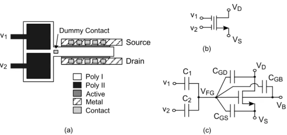
Contact Source Drain Poly I Poly II Active Metal (a) (b) v1 (c) Dummy Contact v2 v1 v2 v1 v2 VS VD C1 C2 CGD CGB CGS VS VD VB VFG
2.1.2 The Quasi-Floating Gate MOS Transistor
The Quasi-Floating gate MOS (QFGMOS) transistor [Ram03] is a device that operates in a very similar way to the FGMOS, but it allows biasing the floating gate at a specific dc voltage while maintaining all the ac properties of the FGMOS. Unlike the FGMOS device, the QFGMOS doesn’t have issues with trapped charge, simulation or new technologies. Figures 2.2 (a) and (b) show a 2-input QFGMOS transistor layout and equivalent circuit, respectively. As in the FGMOS device case, the input terminals V1 and V2 are capacitively coupled to the quasi-floating gate using a second polysilicon layer in order to create capacitors C1 and C2. The dc gate voltage is set to VB independently of the dc levels of the input voltages by weakly connecting the floating gate to a proper dc voltage using a large-valued resistance. This large resistance Rlarge can be implemented by the leakage resistance of a reverse-biased pn junction of a diode-connected MOS transistor operating in cutoff region [Nae03, Ram04, Seo06] as seen in Figure 2.2. Although there are several ways to implement this large valued resistance [Seo06], each of them has advantages and disadvantages. The employed implementation minimizes the dc offset but requires gate voltage swings to be limited to less than a diode turn-on voltage above or below a supply rail voltage, which may be a limitation in ultra low voltage open-loop configurations.
The ac gate voltage at the floating gate in the s-domain is [Ram04]:
(∑ ) (2.3)
where ∑ and CpR is the parasitic capacitance of the large-valued resistive element seen from the gate.
Note from Equation (2.3) that inputs are high-pass filtered with a cutoff frequency 1/(2RlargeCT) which can be made very low (below 1 Hz). Therefore, even for very low frequencies, (2.3) becomes a weighted averaging of the ac input voltages determined by capacitance ratios, plus some parasitic terms. Note also that the exact value of Rlarge or its temperature and voltage dependence are not relevant as long as Rlarge remains large enough to not influencing the circuit’s operation at the lowest frequency required. The exact value of CT is also unimportant.
To VBIAS N-well Rlarge (a) CGD CGB CGS VS VD VB (b) VQFG v1 v2 Drain Source v1 v2 C1 C2 Contact Poly I Poly II Active Metal VBIAS
Figure 2.2. Two-input QFGMOS transistor (a) Layout (b) Equivalent circuit
2.2 Low quiescent current techniques
2.2.1 Class AB operation
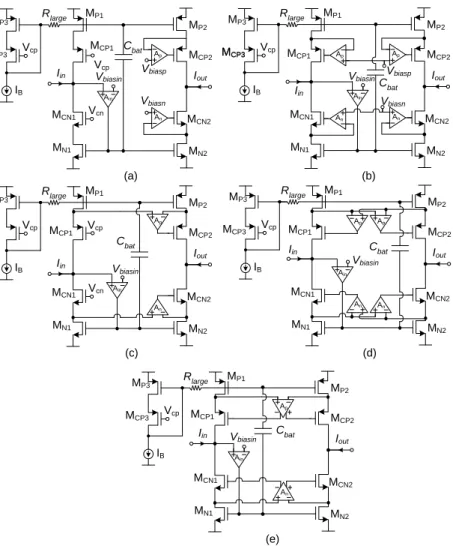
In class A circuits, the signal current swing is limited by the bias current, leading to a tradeoff between dynamic performance and quiescent power consumption. When low power operation is needed, class AB operation can be implemented in order to achieve a similar performance with less power consumption [Kaw96]. There are different ways to implement class AB operation but they usually come with the cost of increasing the transistor count and circuit complexity [Wan90, Pal00]. In this subsection a method to achieve class AB operation using the Quasi-Floating Gate MOS Transistor is explained. The compact implementation of floating dc level shifts achievable by these devices allows obtaining class AB operation in a simple way [Ram06]. Figure 2.3 (a) shows a typical class AB output stage. The quiescent current is set by the bias voltage at node A and the dc level shift Vbat. Under dynamic conditions, signal variations at node A are transferred to node B allowing output currents not limited by the quiescent current. The dc level shift has been implemented in several ways, for instance using diode-connected transistors or resistors biased by dc currents. However, these solutions require extra quiescent power consumption and may increase supply voltage requirements. Moreover, the quiescent current is often not accurately set and dependent on process and temperature variations, and the parasitic elements added by this extra circuitry may limit bandwidth.
Figure 2.3(b) shows an efficient implementation of this dc level shift that avoids these drawbacks, making M2 a QFGMOS transistor [Ram04, Ram06]. In quiescent operation Cbat has no effect and there is not current flowing through Rlarge, so that the quiescent current of the output branch is accurately set to the
bias current IB, regardless of thermal and process variations as it is set by a current mirror. Under dynamic conditions, voltage at node A is transferred to node B after being attenuated by a factor Cbat/(Cbat+CB) and high-pass filtered with cutoff frequency 1/[2πRlarge(Cbat+CB)], where CB is the capacitance at node B. Due to the large resistance employed (in the order of GigaOhms) this cutoff frequency is typically below 1 Hz, so in practice only the dc component of voltage at node A is not transferred to node B. Notice that the implementation of the floating battery does not increase static power or supply voltage requirements. The increase in silicon area is modest as Rlarge is made by a minimum-size MOS transistor (see Section 2.1.2 for more information) and Cbat can be small (with the minimum value imposed by the parasitic capacitance CB).
M
2(a)
M
1V
bat+
A BV
outV
inI
outM
2(b)
M
1C
bat A BV
outV
inI
outR
largeI
BM
BV
BFigure 2.3. Class AB output stage (a) Conventional (b) QFG implementation
2.3 Low voltage techniques
In this section, some techniques aimed to reducing the required supply voltage are briefly described.
2.3.1 Dynamic Cascode biasing
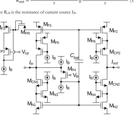
Figure 2.4(a) shows a typical cascode topology. A voltage variation at node A generates a varying current through transistors MN1 and MCN1. As node B is fixed to a constant dc voltage, this current makes voltage at node C to swing as well, modifying the VDS of MN1 and therefore degrading linearity. Moreover, as the current increases, node C voltage decreases, and transistor MN1 can enter into triode region, limiting the dynamic range of the circuit. Figure 2.4 (b) shows a way
to solve this problem [Ram08]. If a floating battery is connected between nodes A and B, node B will track the voltage variations of node A, and therefore, voltage at node C will remain almost constant, increasing linearity and dynamic range.
As in the former section, a compact implementation of the floating battery can be achieved using QFG techniques. Figure 2.4(c) presents the QFGMOS implementation of Figure 2.4(b). MCN1 becomes a QFGMOS transistor. In dc, voltage at node B is set to Vcn because there is not current flowing through Rlarge. Under dynamic conditions, the voltage swing at node A is transferred to node B through the high pass filter formed by Cbat and Rlarge (as explained before, the cutoff frequency is lower than 1 Hz) with a pass band gain of Cbat/(Cbat+CB),where CB is the parasitic capacitance at node B. As the pass band gain should be close to one in order to have the same voltage swing at both nodes, Cbat >> CB. This fact limits Cbat’s minimum value. In this way, the swing experienced by both gates is equal, and therefore, because of the equal current that crosses both transistors, voltage at node C remains approximately constant. Preserving the VDS of MN1 almost constant leads to improved linearity, and allows MN1 to remain in saturation region for a wider input range, increasing dynamic range and allowing a lower voltage operation.
MN1 Iout MCN1 (a) Vcn MN1 MCN1 (c) Cbat Vcn Rlarge Vin Iout Vin MN1 MCN1 (b) Vbat Iout Vin B B B A A A + C C C
Figure 2.4. Wide swing cascode (a) Conventional (b) Dynamic Cascode biasing (c) QFGMOS dynamic cascode biasing implementation
2.3.2 Sub threshold operation: weak inversion
More than 40 years have passed since the first efforts to model the weak inversion operation of a CMOS transistor [Bar72, Tro73, Tro75, Mas74, Bar76] and the first experimental circuits [Vit76, Vit77]. At that time the scientific
community didn’t understand the importance of this topic. In the old times minimum supply voltage requirements were not a problem. Circuit designers were used to design using MOS transistors operating in strong inversion and cascoding stages. Nowadays, due to the fast downscaling of supply voltages in CMOS processes but not so fast downscaling of threshold voltages (see Table 1.1), these design procedures aren’t feasible anymore. Sub-threshold operation enables biasing transistors with very low VGS voltages, allowing lower voltage operation.
At the present time, both hand calculation and circuit simulation of weak inversion transistor are possible. In the circuit simulation domain, the EKV compact MOST model [Enz96b] allows computer accurate calculations for circuits working in weak, moderate and strong inversion. As comparing weak and strong inversion operation using the EKV model would be very complex, it is more convenient to perform the comparison using the hand calculation formulas for two of the most important parameters in transistor design, the drain current and the transconductance gain. Both parameters for saturation operation are shown in Equations (2.4)-(2.5) and (2.6)-(2.7) for weak inversion and strong inversion operation, respectively [Vit77, Enz96a, Vit91, Enz95, Vit03, Wan06].
( ⁄ ) ( ⁄ ) (2.4) (2.5) ( ) (2.6) √ ⁄ (2.7) and ( ) ⁄ (2.8)
where n is the slope factor, is the mobility of electrons near the surface, is
the gate capacitance, W and L are the transistor dimensions, is the threshold
voltage and ⁄ is the thermal voltage.
The previous equations provide some insight about weak inversion operation. Regarding the drain current, the weak inversion model relationship between VGS and ID is exponential, while in the strong inversion model it is
quadratic. With respect to the transconductance, the weak inversion model depends linearly on ID and is independent of while in the strong inversion model the relationship is root-squared and depends on .
The exponential relationship between ID,wi and VGS is very important as it makes possible to design translinear loops [See91] and exponential/log domain circuits [Fre93], achieves maximum Ion/Ioff for a given voltage swing and reduces the intermodulation in RF front ends. The exponential relationship also makes gm/ID larger for weak inversion, achieving maximum intrinsic voltage gain, minimum input noise density, maximum bandwidth, minimum input offset voltage, maximum output noise current and maximum current mismatch dominated by VT mismatch: ⁄ ⁄ for a given kT/C and ID. On top of that, weak inversion operation permits minimum gate voltages, as VGS,wi << VT0 and the saturation drain voltage is as low as 5UT.
The main disadvantage of the weak inversion operation is that as the bias currents are smaller, the speed is also reduced being the transistor cutoff frequency ⁄ . Even though, this bandwidth is enough for some applications (such as the design of Bluetooth Low Energy Zero-IF receivers) and allows very low voltage operation, becoming a very beneficial technique to take into account.
2.3.3 Companding
Companding is a fancy word standing for compressing – expanding. Although the concept was formally introduced in 1990 [Tsi90], companding was extensively used in transmission and storage [Mat34, Bel82] since A. B. Clark of AT&T patented the concept in 1928 [Cla28] and the first report related with its use in analog signal processing circuits dates from 1979 [Ada79].
This technique is based on compressing the input signal dynamic range before processing it, afterwards, the resulting signal dynamic range is expanded again to provide the output signal. The compression block is a non-linear block; Small input signals are amplified while large input signals are attenuated. The expansion block, also non-linear, expand the processed signal in a way that the overall system is kept linear, even though internally it is non-linear. This approach contributes to reduce the overall distortion as the larger inputs are attenuated before processing. On top of that, the signal to noise ratio is improved because the small signals are amplified. Therefore, the dynamic range is enhanced.
![Table 1.1. Downscaling of CMOS processes [Pek04]](https://thumb-us.123doks.com/thumbv2/123dok_us/1871382.2773131/18.688.79.566.652.833/table-downscaling-of-cmos-processes-pek.webp)
![Table 1.3. Radio specifications for Bluetooth and ZigBee in 2.4-GHz ISM Band [Bal10]](https://thumb-us.123doks.com/thumbv2/123dok_us/1871382.2773131/23.688.211.522.582.837/table-radio-specifications-bluetooth-zigbee-ghz-ism-band.webp)