Design, Implementation and Analysis of Error
Tolerant Adder in CMOS 180nm Technology
1Kusumitha M C, 2Shashidhara K S, 3Parameshwara M C 1Student, 2,3Associate Professor
Nitte Meenakshi Institute of Technology
_____________________________________________________________________________________________________
Abstract— The main objective of this work is to design, implement and analyze the error tolerant adder (ETA) for DSP applications. This paper aims at designing ETA using low power and energy efficient one-bit full adders. Further we analyze ETA using state of the art one-bit full adders. All the ETA under consideration are designed by using CMOS 180nm technology. The design metrics such as power, delay, PDP and area in terms of transistor count are extracted under common Process-Voltage-Temperature (PVT) conditions. These design metrics are extracted for inputs signal frequency of 200MHz supply voltage of 1.8V and temperature of. All simulations are carried out using Cadence Spectre Simulator using BSIM Version 3 MOSFET models.
Index Terms— Adder, Delay, Power, PDP, ETA
_____________________________________________________________________________________________________
I. INTRODUCTION
The rapid advancements in VLSI technology due to continuous scaling will result in billions of devices and thousands of defects [1]. Further the advancement of VLSI process technology approaches the physical limits, process variations and quantum effects of nanometer circuits. Thus, manufacturing defect free chips is challenging. The traditional techniques to enhance the yield are fault and defect tolerance which have become inadequate. Thus, the importance of error-tolerance has received much attention in the current technology [2]. This results in low yield chips. A new way to enhance yield is error-tolerance [3]. A circuit is said to be error tolerant with respect to an application if it contains defects that cause internal and may cause external errors, and (2) the system that incorporates this circuit produces acceptable results.
The need for error-tolerance was foretold in the 2003 International Technology Roadmap for Semiconductors (ITRS) [4], where it was stated that “relaxing the requirement of 100% correctness in both transient and permanent failures of signals, logic values, devices, or interconnects may reduce the cost of manufacturing, verification and testing.” How to cost-effectively identify acceptable defective chips is one of the central themes in this emerging field. Several attributes have been employed to evaluate the acceptability of defective chips and some corresponding measurement methods have also been developed in previous work. One of these attributes is error-rate [5].
Error tolerance (ET) scheme was proposed to increase effective yield. ET is a new design and test paradigm, which takes into consideration whether erroneous outputs of defective circuits produce acceptable results. ET classifies a chip as being acceptable/unacceptable by estimating the performance degradation due to faults, rather than relying solely on the conventional perfect/imperfect classification. ET analyzes the system-level effects of faults, and accepts chips if the performance degradation they lead to is within some, application-specific, ranges of acceptability [6].
Increasingly huge data sets and the need for instant response require the adder to be large and fast. The traditional ripple-carry adder (RCA) is therefore no longer suitable for large adders because of its low-speed performance. Many different types of fast adders, such as the carry-skip adder (CSK), carry-select adder (CSL), and carry-look-ahead adder (CLA) have been developed. Also, there are many low-power adder design techniques that have been proposed. However, there are always trade-offs between speed and power. The error-tolerant design can be a potential solution to this problem. By sacrificing some accuracy, the “error-tolerant-adder” (ETA) can attain great improvement in both the power consumption and speed performance [7].
II. ADDITION ARITHMETIC IN ETA
In a conventional adder circuit, the delay is mainly attributed to the carry propagation chain along the critical path, from the Least Significant Bit (LSB) to the Most Significant Bit (MSB). Meanwhile, a significant proportion of the power consumption of an adder is due to the glitches that are caused by the carry propagation. Therefore, if the carry propagation can be eliminated or curtailed, a great improvement in speed performance and power consumption can be achieved.
To minimize error due to the elimination of the carry chain
Check every bit position from left to right (MSB -LSB) starting from right of demarcation line. If both input bits are "0" or different, normal one-bit addition is performed and the operation, Proceeds to next bit position. The checking process is stopped when both input bits are encountered as high i.e., 1, and from this bit onwards, all sum bits to the right (LSB) are set to "1." This is how this adder Saves carry propagation delay and enhances the overall performance. An example for addition arithmetic is as shown in figure 1.
Figure 1, the two 16-bit input operands, A= “1011001110011010” (45978) and B= “0110100100010011” (26899), are divided equally into 8 bits each for the accurate and inaccurate parts.
Fig 1: An example of addition arithmetic in ETA
The example given in Figure 1 should actually yield “10001110010101101” (72877) if normal arithmetic has been applied. The overall error generated can be computed as OE = 72877-72863=14. By eliminating the carry propagation path in the inaccurate part and performing the addition in two separate parts simultaneously, the overall delay time is greatly reduced, so is the power consumption.
III. DESIGN OF ERROR TOLERANT ADDER
Architecture of the error tolerant adder is shown in the figure 2. This is the most straight forward structure consists of two parts an accurate part and inaccurate part. The accurate part is constructed using the conventional adder such as the ripple carry adder. The carry-in of this accurate part is connected to ground. The inaccurate part constitutes of two blocks a carry free addition block and a control block. The control block is used to generate the control signals to determine the working mode of the carry-free addition block
Fig 2: Architecture of ETA
IV. DESIGN OF ACCURATE PART
Ripple carry addition is the most power saving conventional addition technique. The ripple carry adder is built from cascading the full adders in series. It is used for addition logic in the accurate part. Hence each bit gets rippled in to the next stage. In a ripple carry adder the sum and carryout bits of any half adder stage is not valid until the carry in of the stage occurs. The propagation delay inside the logic circuitry is the reasons behind this, propagation delay is the time elapsed between the application of an input and occurrence of the corresponding output. Each block of the ripple carry adder is designed using conventional adder which is discussed in section 7.
V. DESIGN OF INACCURATE PART
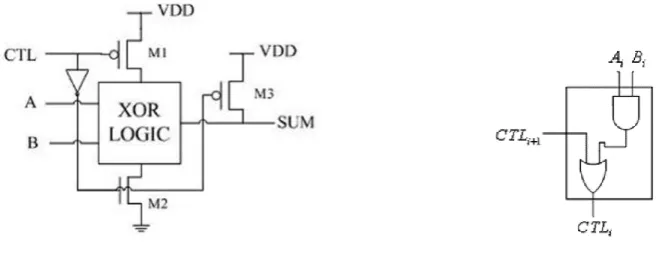
The inaccurate part is the most critical section in the ETA as it determines the accuracy, speed performance, and power consumption of the adder. The inaccurate part consists of two blocks: the carry-free addition block and the control block. The carry-free addition block is made up of modified XOR gates, and each of which is used to generate a sum bit. The carry-free addition block is designed using modified XOR gates to generate a sum bit individually for LSBs. The function of the control block is to detect the first bit position when both input bits are “1,” and to set the control signal CTL to high at this position as well as those to its right up to LSB. The block diagram of the carry free addition block and the schematic implementation of the modified XOR gate is shown in figure 3 and its control logic block is shown in figure 4.
Fig. 3: Modified XOR Gate Fig. 4: Control Block The modified XOR gates are then combined together to obtain the carry free addition block as shown the figure 5.
Fig 5: Architecture of Carry-Free Addition Block
VI. SIMULATION ENVIRONMENT
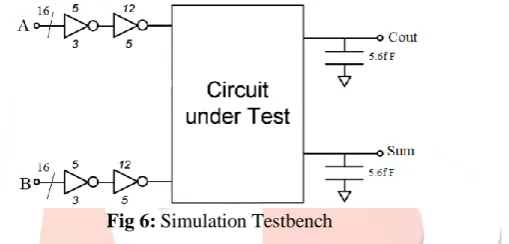
The “design metrics” (DMs) such as delay, power, and PDP are extracted by applying standard test input patterns as shown in the figure 6 along with the transistor sizing of each buffer. To extract the DMs the input signals having frequency of 200 MHz and supply voltage of 1.8 V are applied through input buffers (to generate realistic input signals) for the “circuit under test” (CUT). The CUT outputs are connected to the load capacitance of 5.6 fF (to have realistic load conditions). Standard test input patterns is applied and delay and power is extracted and it is as shown in the figure 6 along with the transistor sizing of each buffer.
Fig 6: Simulation Testbench VII. RESULTS AND DISCUSSION
Based on the dividing strategy used depending on the size of Accurate Sum Part (ASP) and Inaccurate Sum Part (ISP) the following ETA’s have been designed and analysed in terms of design metrics. In this paper Error tolerant adder is designed for four different combinations as shown in the table 1.
Table1: Design Metrics Adder ASP ISP ETA 1 8-Bit 8-Bit ETA 2 6-Bit 10-Bit ETA 3 4-Bit 12-Bit ETA 4 2-Bit 14-Bit
Accurate Sum Part is designed using various one-bit full adders [8]-[10] in CMOS 180nm technology and the DMs power consumption, delay and area of the adder are tabulated in table below.
1.ETA 1
In ETA1 the length of accurate part is 8 bit and length of inaccurate part is 8 bit. Accurate part is designed by connecting eight 1-bit full adders in series as shown in figure 7. Inaccurate part is designed using CMOS logic based XOR gate as shown in figure 7.
Fig 7: Architecture of ETA 1
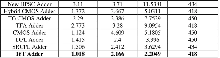
Among all the adder 16T adder gives the less delay and low power and hence less PDP. It consumes 418 transistors. Simulation result is tabulated in table 2.
Table 2: Simulation Result for ETA 1
ETA Delay (n sec) Power (m W) PDP (pJ) Transistor Count
New HPSC Adder 3.11 3.71 11.5381 434
Hybrid CMOS Adder 1.372 3.667 5.0311 418
TG CMOS Adder 2.29 3.386 7.7539 450
TFA Adder 2.773 3.28 9.0954 418
CMOS Adder 1.124 4.609 5.1805 450
DPL Adder 1.415 2.4 3.396 450
SRCPL Adder 1.506 2.412 3.6294 434
16T Adder 1.018 2.166 2.2049 418
2.ETA 2
In ETA 2 the length of accurate part is 6 bit and length of inaccurate part is 10 bit. Accurate part is designed by connecting six 1-bit full adders in series as shown in figure 8. Inaccurate part is designed using CMOS logic based XOR gate as shown in figure 8.
Fig 8: Architecture of ETA 2
Among all the adder 16T adder gives the less delay and low power and hence less PDP and area consumed is calculated in terms of transistor count, it consumes 428 transistors as shown in the table 3 below.
Table 2: Simulation Result for ETA 2
ETA Delay (n sec) Power (m W) PDP (pJ) Transistor Count
HPSC Adder 0.8424 3.316 2.7933 416
New HPSC Adder 2.21 3.156 6.9747 440
Hybrid CMOS Adder 0.9789 3.15 3.0835 428
TG CMOS Adder 1.614 2.873 4.637 452
TFA Adder 1.887 2.818 5.3175 428
CMOS Adder 0.8301 3.663 3.0406 452
DPL Adder 1.024 2.239 2.2927 452
SRCPL Adder 1.086 2.247 2.24402 440
16T Adder 0.7614 2.052 1.5623 428
3.ETA 3
In ETA 3 the length of accurate part is 4 bit and length of inaccurate part is 12 bit. Accurate part is designed by connecting four 1-bit full adders in series as shown in figure. Inaccurate part is designed using CMOS logic based XOR gate as shown in figure 9.
Fig 9: Architecture of ETA 3
Among all the adder 16T adder gives the less delay and low power and hence less PDP and area consumed is calculated in terms of transistor count, it consumes 438 transistors as shown in the table 4 below.
Table 4: Simulation Result for ETA 3
ETA Delay (p sec) Power (m W) PDP (pJ) Transistor Count
HPSC Adder 532 3.314 1.7630 430
New HPSC Adder 1310 3.161 4.1409 446
Hybrid CMOS Adder 585.4 3.191 1.8680 438
TG CMOS Adder 936.4 2.971 2.7820 454
TFA Adder 997.5 2.932 2.9246 438
CMOS Adder 535.7 3.489 1.8690 454
DPL Adder 633.4 2.523 1.5980 454
SRCPL Adder 664.9 2.534 1.6848 446
4.ETA 4
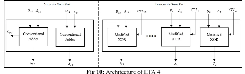
In ETA 4 the length of accurate part is 2 bit and length of inaccurate part is 14 bit. Accurate part is designed by connecting two 1-bit full adders in series as shown in figure. Inaccurate part is designed using CMOS logic based XOR gate as shown in figure 10.
Fig 10: Architecture of ETA 4
Among all the adder 16T adder gives the less delay and low power and hence less PDP and area consumed is calculated in terms of transistor count, it consumes 448 transistors as shown in the table 5 below.
Table 4: Simulation Result for ETA 3
ETA Delay (p sec) Power (m W) PDP (pJ) Transistor Count
HPSC Adder 247.2 3.046 0.7529 444
New HPSC Adder 419.1 2.988 1.2522 452
Hybrid CMOS Adder 238.8 2.988 0.7135 448
TG CMOS Adder 280.4 2.906 0.8148 456
TFA Adder 268.4 2.903 0.7791 448
CMOS Adder 241.8 3.106 0.7510 456
DPL Adder 248.9 2.718 0.6765 456
SRCPL Adder 249.9 2.722 0.6802 452
16T Adder 240.2 2.67 0.6413 448
VIII. CONCLUSION
In this paper the simulation of ETA design is carried out using standard Cadence Virtuoso tools with 180 nm technology and compared its performance with other designs. The simulation results established that the 16T adder offered improved PDP compared with the earlier reports. The ETA design based on 16T adder is found to be low power and has an average power dissipation at input signal frequency of 200 MHz, supply voltage of 1.8 V, and load capacitance of 5.6 fF.
REFERENCES
[1] M. A. Breuer, “Intelligible test techniques to support error-tolerance,” in Proc. Asian Test Symp., Nov. 2004, pp. 386– 393.
[2] K. J. Lee, T. Y. Hsieh, and M. A. Breuer, “A novel testing methodology based on rate to support error-tolerance,” in Proc. Int. Test Conf., 2005, pp. 1136–1144.
[3] A. B. Melvin and Z. Haiyang, “Error-tolerance and multi-media,” in Proc. 2006 Int. Conf. Intell. Inf. Hiding and Multimedia Signal Process., 2006, pp. 521–524.
[4] http://www.itrs2.net/itrs-reports/ 2014 ITRS.html
[5] T. Y. Hsieh, K. J. Lee, and M. A. Breuer, “Reduction of detected acceptable faults for yield improvement via error-tolerance,” in Proc. Des., Automation and Test Eur. Conf. Exhib., 2007, pp. 1–6.H. Chung and A. Ortega, “Analysis and testing for error tolerant motion estimation,” in Proc. Defect and Fault Tolerance in VLSI Syst. Symp., 2005, pp. 514–522.
[6] H. Chung and A. Ortega, “Analysis and testing for error tolerant motion estimation,” in Proc. Defect and Fault Tolerance in VLSI Syst. Symp.,2005, pp. 514–522.
[7] Ning Zhu, Wang Ling Goh, Weija Zhang, Kiat Seng Yeo, and Zhi Hui Kong “Design of Low-Power High-Speed Truncation-Error-Tolerant Adder and Its Application in Digital Signal Processing”, IEEE Transactions on Very Large Scale Integration (VLSI) Systems, Vol. 18, No. 8, August 2010
[8] Partha Bhattacharyya, Bijoy Kundu, Sovan Ghosh, Vinay Kumar and Anup Dandapat, “Performance Analysis of a Low-Power High-Speed Hybrid 1-bit Full Adder Circuit”, IEEE Transactions on Very Large Scale Integration (VLSI) Systems, Vol. 23, NO. 10, October 2015
[9] Ahmed M. Shams, Tarek K. Darwish and Magdy A. Bayoumi, “Performance Analysis of Low-Power 1-Bit CMOS Full Adder Cells”, IEEE Transactions on Very Large Scale Integration (VLSI) Systems, VOL. 10, NO. 1, February 2002
[10]R.P.Meenaakshi Sundari, Dr.R.Anita, M.K.Anandkumar, “Implementation of Low Power CMOS Full Adders Using Pass Transistor Logic”, IOSR Journal of VLSI and Signal Processing (IOSR-JVSP) Volume 2, Issue 5 (May. – Jun. 2013), PP 38-43 e-ISSN: 2319 – 4200, p-ISSN No.: 2319 – 4197