A COMPREHENSIVE ANALYSIS OF
SPACE VECTOR PWM TECHNIQUE
BASED ON PLACEMENT OF
ZERO-SPACE VECTOR
G.SAMBASIVA RAO
Dept. of Electrical Engg, R.V.R & J.C College of Engg, Chowdavaram, Guntur -522 019(India)
Dr.K.CHANDRA SEKHAR
Dept. of Electrical Engg, R.V.R & J.C College of Engg, Chowdavaram, Guntur -522 019(India)
Abstract:
In this paper, the effect of placement of zero-space vector for the implementation of space vector based Pulse Width Modulation techniques for 3-phase Voltage Source Inverter is presented. Several pulse width modulation (PWM) control strategies have been proposed for 3-phase voltage source inverter (VSI) in the past. It is known that space vector modulation (SVM) offers a degree of freedom in its implementation with regard to the placement of the zero-space vector. Apart from constructing a consistent theoretical framework, simulation results with conventional continuous SVM and various discontinuous SVM techniques are presented and all the cases are compared in this paper.
Keywords: space vector modulation, continuous SVM, discontinuous SVM, zero-space vector, effective time.
1.Introduction
In order to efficiently achieve high-quality sinusoidal output voltages, a deep understanding of modulation schemes and mathematical methodologies that can be applied to determine various combinations for switching the inverter’s power devices ON or OFF is essential. There are some requirements for a PWM method. Among them, full utilization of the DC-bus voltage is extremely important to achieve the maximum output torque under all operating conditions for AC machine drive applications and to obtain the control voltage margin, the minimization of the current ripple and/or the total losses of the power converter system and, needless to say, the whole modulation task should have the simplest form to be easily applied in actual applications. In this aspect, compared with any other PWM method for the VSI, the PWM method based on voltage space vectors results in excellent DC bus utilization[1][2].
The effect of placement of the zero-space vector time period in a sampling time interval and the
implementation of a generalized space vector modulation scheme for a two-level inverter have extensively been investigated in [3]. In [3], it is shown that the centric placement of the block comprising the active vectors in a given sampling time interval would achieve a better spectral performance compared to the cases, where that block is not kept at the center. The flexibility in the placement of the zero-space vector imparts a generality to the space vector based PWM techniques and results in either center-spaced (continuous) or discontinuous
(non-center spaced) PWM methods. In discontinuous PWM method one of the phases is clamped to DC rail for 1200 .
In the proposed PWM method, the actual gating times for each inverter arm are immediately deduced, simply by using the “effective time” relocation algorithm [4]. Furthermore, by employing one degree of freedom
that allows the effective time to be relocated anywhere within the sampling interval, the 150 discontinuous SVM,
300 discontinuous SVM, 600 discontinuous SVM and 1200 discontinuous SVM methods are simulated using
MATLAB. The widely used overmodulation scheme is also be implemented by the effective time concept. As well as giving a detailed explanation of the proposed SVM algorithms, the simulation results are presented in this paper.
2. Space Vector Modulation Implementation
The standard topology of a 3-phase VSI is shown in Fig.1 (a), and consists of three phase legs with two switches per leg, arranged so that each phase output can be connected to either the upper or the lower DC bus as desired. In Fig. 1(b), the eight available different switching vectors of the inverter are depicted with the space vector concept [2]. The switching state “1” means the firing for the upper device of one arm and the pole voltage(Vao,Vbo,Vco) will have half of the DC-link voltage value.
Fig.1 (a). Three-phase inverter system Fig.1 (b). Space vector diagram of the available switching vectors.
Note that the switching states of each arm should be combined with each other to compose the required three-phase output voltage. Because each pole voltage has only two levels according to the related switching state, the time duration in which the different voltages are maintained is definitely related to the voltage modulation task. Therefore, the modulation task can be greatly simplified by considering the relation between the time duration and the output voltage [4].
Fig.2. Actual gating time generation for continuous SVM
sampling time and Teff denotes the time duration in which the different voltage is maintained. Teff is called the “effective time”. For the purpose of explanation, an imaginary time value will be introduced [4] as follows:
Vxs
*
Vdc
Ts
Txs
,(x=a,b,c) (1)Vas*,Vbs*and Vcs* are the A-phase, B -phase, and C-phase reference voltages, respectively. This switching time could be negative in the case where negative phase voltage is commanded. Therefore, this time is called the “imaginary switching time”.
Now, the effective time can be defined as the time duration between the minimum and the maximum value of three imaginary times, as given by
Teff =Tmax-Tmin Where Tmin = min(Tas,Tbs,Tcs)
Tmax = max (Tas,Tbs,Tcs). (2)
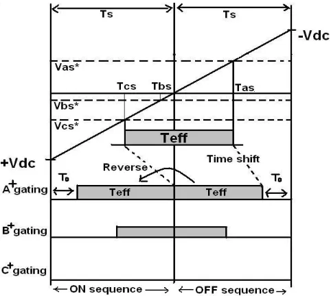
When the actual gating signals for power devices are generated in the PWM algorithm, there is one degree of freedom by which the effective time can be relocated anywhere within the sampling interval. Therefore, a time-shifting operation will be applied to the imaginary switching times to generate the actual gating times (Tga,Tgb,Tgc ) for each inverter arm, as shown in Fig. 2. This task is accomplished by adding the same value to the imaginary times as follows:
Tga=Tas+Toffset Tgb=Tbs+Toffset
Tgc=Tcs+Toffset (3) Where Toffset is the ‘offset time’
This gating time determination task is only performed for the sampling interval in which all of the switching states of each arm go to 0 from 1. This interval is called the “OFF sequence”. In the other sequence, it is called the “ON sequence.” In order to generate a symmetrical switching pulse pattern within two sampling intervals, the actual switching time will be replaced by the subtraction value, with sampling time as follows: Tga=Ts-Tga
Tgb=Ts-Tgb
Tgc=Ts-Tgc (4)
2.1 Continuous SVM:
There is one degree of freedom by which the effective time can be relocated anywhere within the sampling interval. To force the effective time period block to be exactly at the center of the sampling time interval as shown in Fig.2 is given by [4]
Toffset1=
2
To
-Tmin (5)
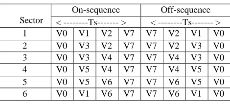
Where To is the time duration for which the zero-vector combination is switched. The detailed switching arrangement is given in Table1.
Table 1. Switching arrangement for continuous SVM
Sector
On-sequence Off-sequence < ---Ts--- > < ---Ts--- >
1 V0 V1 V2 V7 V7 V2 V1 V0
2 V0 V3 V2 V7 V7 V2 V3 V0
3 V0 V3 V4 V7 V7 V4 V3 V0
4 V0 V5 V4 V7 V7 V4 V5 V0
5 V0 V5 V6 V7 V7 V6 V5 V0
6 V0 V1 V6 V7 V7 V6 V1 V0
2.2 Discontinuous SVM:
In this PWM scheme , one of the three inverter output legs is clamped to either positive or negative DC bus
without any switchings for 1200 interval of electrical fundamental period. In all discontinuous PWM(DPWM)
techniques, the total duration of clamping per phase is 120 electrical degrees, but for 600,300 and 150 DPWM the
the references to either the positive or negative rail exclusively, 600,300 and 150 DPWM use both DC bus rails. The principle of this PWM scheme can be depicted in terms of effective time as follows. If the A-phase voltage reference is positive and has maximum magnitude, the A-phase switch should be fixed to the ON state. Then the offset time to be added is:
Toffset2=Ts-Tmax (6)
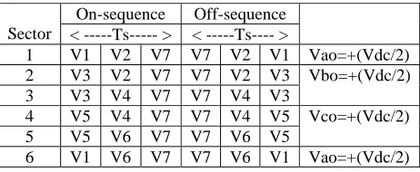
With this offset time “eq.(6)” the effective time period block is placed at the end(or trailing edge)of the sampling time interval as shown in fig.3 and switching arrangement is given in Table 2. In this scheme, every
phase leg is clamped to upper DC rail for 1200as shown in Table 2.This type of discontinuous switching pattern
is termed as DPWMAX [6].
Fig.3. Actual gating time generation for DPWMAX
Table 2. Switching arrangement for DPWMAX
Sector
On-sequence Off-sequence < ---Ts--- > < ---Ts---- >
1 V1 V2 V7 V7 V2 V1 Vao=+(Vdc/2)
2 V3 V2 V7 V7 V2 V3 Vbo=+(Vdc/2)
3 V3 V4 V7 V7 V4 V3
4 V5 V4 V7 V7 V4 V5 Vco=+(Vdc/2)
5 V5 V6 V7 V7 V6 V5
6 V1 V6 V7 V7 V6 V1 Vao=+(Vdc/2)
If the A-phase voltage reference is negative and has maximum magnitude, the A-phase switch should be fixed to the OFF state. Then the offset time to be added is:
Toffset3= -Tmin (7)
With this offset time “eq.(7)” the effective time period block is placed at the beginning(or leading edge)of the sampling time interval as shown in Fig.4 and switching arrangement is given in Table 3. In this
scheme every phase leg is clamped to lower DC rail for 1200as shown in Table 3.This type of discontinuous
switching pattern is termed as DPWMIN [6].
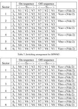
There are three different ways of realizing 60º discontinuous modulation: 30º lagging clamp termed as DPWM2, 30º leading clamp termed as DPWM0, and 0º clamp termed as DPWM1 [6]. The clamp phase offset relates to where the non-switching periods of each phase leg are positioned relative to the peak of the fundamental voltage waveform [6]. The switching arrangement for three schemes is given in Table 4 to Table 6. In Table 4 and Table 7 “y” represents sector number, y1 indicates first half of the “y” sector and y2 indicates second half of the “y” sector.
The 30º and 150discontinuous modulation strategies termed as DPWM3 [6] and DPWM4. Each method
calls for a successive inverter phase leg to be unmodulated for 30º and150 of the fundamental, alternating
indicates first quarter of the “y” sector, y2 indicates second quarter of the “y” sector, y3 indicates third quarter of the “y” sector and y4 indicates fourth quarter of the “y” sector.
Fig.4. Actual gating time generation for DPWMIN
Table 3. Switching arrangement for DPWMIN
Sector
On-sequence Off-sequence < ---Ts---- > < ---Ts---- >
1 V0 V1 V2 V2 V1 V0 Vco=-(Vdc/2)
2 V0 V3 V2 V2 V3 V0
3 V0 V3 V4 V4 V3 V0 Vao=-(Vdc/2)
4 V0 V5 V4 V4 V5 V0
5 V0 V5 V6 V6 V5 V0 Vbo=-(Vdc/2)
6 V0 V1 V6 V6 V1 V0
Table 4.Switching arrangement for DPWM2
Table 5.Switching arrangement for DPWM0
Sector
On-sequence Off-sequence < ---Ts--- > < ---Ts---- >
1 V1 V2 V7 V7 V2 V1 Vao=+(Vdc/2)
2 V0 V3 V2 V2 V3 V0 Vco=-(Vdc/2)
3 V3 V4 V7 V7 V4 V3 Vbo=+(Vdc/2)
4 V0 V5 V4 V4 V5 V0 Vao=-(Vdc/2)
5 V5 V6 V7 V7 V6 V5 Vco=+(Vdc/2)
6 V0 V1 V6 V6 V1 V0 Vbo=-(Vdc/2)
Sector
On-sequence Off-sequence < ---Ts---- > < ---Ts---- >
1 V0 V1 V2 V2 V1 V0 Vco=-(Vdc/2)
2 V3 V2 V7 V7 V2 V3 Vbo=+(Vdc/2)
3 V0 V3 V4 V4 V3 V0 Vao=-(Vdc/2)
4 V5 V4 V7 V7 V4 V5 Vco=+(Vdc/2)
5 V0 V5 V6 V6 V5 V0 Vbo=-(Vdc/2)
Table 6.Switching arrangement for DPWM1
Sector
On-sequence Off-sequence < ---Ts---- > < ---Ts---- >
1
11 V1 V2 V7 V7 V2 V1 Vao=+(Vdc/2) 12 V0 V1 V2 V2 V1 V0 Vco=-(Vdc/2)
2
21 V0 V3 V2 V2 V3 V0
22 V3 V2 V7 V7 V2 V3 Vbo=+(Vdc/2)
3
31 V3 V4 V7 V7 V4 V3
32 V0 V3 V4 V4 V3 V0 Vao=-(Vdc/2)
4
41 V0 V5 V4 V4 V5 V0
42 V5 V4 V7 V7 V4 V5 Vco=+(Vdc/2)
5
51 V5 V6 V7 V7 V6 V5
52 V0 V5 V6 V6 V5 V0 Vbo=-(Vdc/2)
6
61 V0 V1 V6 V6 V1 V0
62 V1 V6 V7 V7 V6 V1 Vao=+(Vdc/2)
Table 7. Switching arrangement for DPWM3
Table 8.Switching arrangement for DPWM4
Table 8(continued) Sector
On-sequence Off-sequence < ---Ts---- > < ---Ts---- >
1
11 V0 V1 V2 V2 V1 V0 Vco=-(Vdc/2) 12 V1 V2 V7 V7 V2 V1 Vao=+(Vdc/2)
2
21 V3 V2 V7 V7 V2 V3 Vbo=+(Vdc/2) 22 V0 V3 V2 V2 V3 V0 Vco=-(Vdc/2)
3
31 V0 V3 V4 V4 V3 V0 Vao=-(Vdc/2) 32 V3 V4 V7 V7 V4 V3 Vbo=+(Vdc/2)
4
41 V5 V4 V7 V7 V4 V5 Vco=+(Vdc/2) 42 V0 V5 V4 V4 V5 V0 Vao=-(Vdc/2)
5
51 V0 V5 V6 V6 V5 V0 Vbo=-(Vdc/2) 52 V5 V6 V7 V7 V6 V5 Vco=+(Vdc/2)
6
61 V1 V6 V7 V7 V6 V1 Vao=+(Vdc/2) 62 V0 V1 V6 V6 V1 V0 Vbo=-(Vdc/2)
Sector
On-sequence Off-sequence < ---Ts---- > < ---Ts---- >
1
11 V0 V1 V2 V2 V1 V0 Vco=-(Vdc/2) 12 V1 V2 V7 V7 V2 V1 Vao=+(Vdc/2) 13 V0 V1 V2 V2 V1 V0 Vco=-(Vdc/2) 14 V1 V2 V7 V7 V2 V1 Vao=+(Vdc/2)
2
21 V3 V2 V7 V7 V2 V3 Vbo=+(Vdc/2) 22 V0 V3 V2 V2 V3 V0 Vco=-(Vdc/2) 23 V3 V2 V7 V7 V2 V3 Vbo=+(Vdc/2) 24 V0 V3 V2 V2 V3 V0 Vco=-(Vdc/2)
3
31 V0 V3 V4 V4 V3 V0 Vao=-(Vdc/2) 32 V3 V4 V7 V7 V4 V3 Vbo=+(Vdc/2) 33 V0 V3 V4 V4 V3 V0 Vao=-(Vdc/2) 34 V3 V4 V7 V7 V4 V3 Vbo=+(Vdc/2)
4
41 V5 V4 V7 V7 V4 V5 Vco=+(Vdc/2) 42 V0 V5 V4 V4 V5 V0 Vao=-(Vdc/2) 43 V5 V4 V7 V7 V4 V5 Vco=+(Vdc/2) 44 V0 V5 V4 V4 V5 V0 Vao=-(Vdc/2)
5
51 V0 V5 V6 V6 V5 V0 Vbo=-(Vdc/2) 52 V5 V6 V7 V7 V6 V5 Vco=+(Vdc/2) 53 V0 V5 V6 V6 V5 V0 Vbo=-(Vdc/2)
6
61 V1 V6 V7 V7 V6 V1 Vao=+(Vdc/2) 62 V0 V1 V6 V6 V1 V0 Vbo=-(Vdc/2) 63 V1 V6 V7 V7 V6 V1 Vao=+(Vdc/2) 64 V0 V1 V6 V6 V1 V0 Vbo=-(Vdc/2)
3.Simulation Results And Discussion
The proposed PWM switching strategies are simulated using MATLAB for a 4KW, 3-phase induction motor in open loop with v/f control. The pole voltage Vao, normalized harmonic spectrums of pole voltage, phase voltage and stator current with no load are presented for continuous SVM, DPWMAX, DPWMIN, DPWM2, DPWM0, DPWM1, DPWM3 and DPWM4 in Fig.5,Fig.6,Fig.7, Fig.8, Fig.9, Fig.10, Fig.11 and Fig.12 respectively with modulation index 0.7. The waveforms depicts that the placement of zero-vector influences the voltage spectrum, harmonic content and ripple in the current. The continuous SVM gives better spectral performance compared to discontinuous SVM techniques. In DPWMAX and DPWMIN discontinuous modulation, the pole voltage is not half-wave symmetric and contains the dc component. The other
discontinuous modulation schemes have half-wave symmetry. In 600 discontinuous modulation schemes the
each phase is clamped for 600 to positive DC rail and other 600 to negative DC rail over the fundamental period.
In 300 discontinuous modulation schemes the each phase is clamped two times for 300 to positive DC rail and
clamped two times for 300 to negative DC rail over the fundamental period. In 150 discontinuous modulation
schemes the each phase is clamped four times for 150 to positive DC rail and clamped four times for 150 to
negative DC rail over the fundamental period.
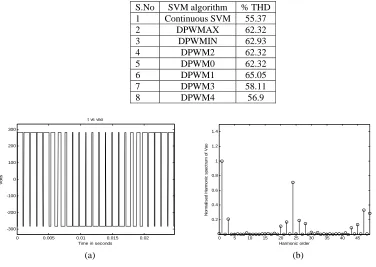
The total harmonic distortion (THD) of the motor phase voltage (based on the data up to the first 50 harmonics) for all the variants of the PWM scheme presented in this paper and are tabulated in Table 9. From the analysis the THD of continuous SVM outperforms the others.
Table 9. THD of the motor phase voltage
S.No SVM algorithm % THD
1 Continuous SVM 55.37
2 DPWMAX 62.32
3 DPWMIN 62.93
4 DPWM2 62.32
5 DPWM0 62.32
6 DPWM1 65.05
7 DPWM3 58.11
8 DPWM4 56.9
0 0.005 0.01 0.015 0.02
-300 -200 -100 0 100 200 300
t vs vao
Time in seconds
Vo
lt
s
0 5 10 15 20 25 30 35 40 45
0.2 0.4 0.6 0.8 1 1.2 1.4
Harmonic order
N
or
m
al
is
e
d H
a
rm
o
ni
c
s
p
ec
tr
um
o
f V
ao
0 5 10 15 20 25 30 35 40 45 0 0.5 1 1.5 Harmonic order N o rm al is ed H a rm on ic s p ec tr u m o f Ph as e v o lt ag e
9000 9500 10000 10500 -50 -40 -30 -20 -10 0 10 20 30 40 50 (c) (d)
Fig.5.Results for Continuous SVM (a)pole voltage, Vao (b) Normalized harmonic spectrum of pole voltage (c) Normalized harmonic spectrum of phase voltage, Vas (d) phase current.
0 0.005 0.01 0.015 0.02
-300 -200 -100 0 100 200 300
t vs vao
Time in seconds
Vo
lt
s
0 5 10 15 20 25 30 35 40 45
0.2 0.4 0.6 0.8 1 1.2 1.4 Harmonic order N or m al is ed H ar m oni c s pec tr um o f V ao
(a) (b)
0 5 10 15 20 25 30 35 40 45
0 0.5 1 1.5 Harmonic order N o rm a lis ed H ar m o ni c s p ec tr um o f P ha s e v o lt ag e
1.16 1.18 1.2 1.22 1.24 1.26 1.28 1.3 1.32
x 104 -60 -40 -20 0 20 40 60 (c) (d)
Fig.6.Results for DPWMAX (a) pole voltage, Vao (b) Normalized harmonic spectrum of pole voltage (c) Normalized harmonic spectrum of phase voltage, Vas (d) phase current.
0 0.005 0.01 0.015 0.02 -300 -200 -100 0 100 200 300
t vs vao
Time in seconds
Vo
lt
s
0 5 10 15 20 25 30 35 40 45 0.2 0.4 0.6 0.8 1 1.2 1.4 Harmonic order N or m al is e d H ar m oni c s pec tr um o f V a o
0 5 10 15 20 25 30 35 40 45 0 0.5 1 1.5 Harmonic order N or m al is ed H ar m oni c s pec tr um of Phas e v o lt age
1.16 1.18 1.2 1.22 1.24 1.26 1.28 1.3 1.32 x 10⁴
-60 -40 -20 0 20 40 60
(c) (d)
Fig.7.Results for DPWMIN (a)pole voltage, Vao (b) Normalized harmonic spectrum of pole voltage (c) Normalized harmonic spectrum of phase voltage, Vas (d) phase current.
0 0.005 0.01 0.015 0.02
-300 -200 -100 0 100 200 300
t vs vao
Time in seconds
Vo
lt
s
0 5 10 15 20 25 30 35 40 45
0.2 0.4 0.6 0.8 1 1.2 1.4 Harmonic order N o rm a lise d H a rm o n ic sp e c tr u m o f V a o
(a) (b)
0 5 10 15 20 25 30 35 40 45
0 0.5 1 1.5 Harmonic order N o rm a lis ed H ar m o ni c s p ec tr um o f P ha s e v o lt ag e
0.9 0.95 1 1.05 1.1
x 104
-60 -40 -20 0 20 40 60 (c) (d)
Fig.8.Results for DPWM2 (a) pole voltage, Vao (b) Normalized harmonic spectrum of pole voltage (c) Normalized harmonic spectrum of phase voltage, Vas (d) phase current.
0 0.005 0.01 0.015 0.02
-300 -200 -100 0 100 200 300
t vs vao
Time in seconds
Vo
lt
s
0 5 10 15 20 25 30 35 40 45
0.2 0.4 0.6 0.8 1 1.2 1.4 Harmonic order N or m al is e d H a rm o ni c s p ec tr um o f V ao
0 5 10 15 20 25 30 35 40 45 0 0.5 1 1.5 Harmonic order N o rm al is ed H ar m on ic s p ec tr u m o f Ph as e v o lt ag e
0.9 0.95 1 1.05 1.1 x 10⁴ -60 -40 -20 0 20 40 60
(c) (d)
Fig.9.Results for DPWM0 (a) pole voltage, Vao (b) Normalized harmonic spectrum of pole voltage (c) Normalized harmonic spectrum of phase voltage, Vas (d) phase current.
0 0.005 0.01 0.015 0.02 -300 -200 -100 0 100 200 300
t vs vao
Time in seconds
Vol
ts
0 5 10 15 20 25 30 35 40 45 0.2 0.4 0.6 0.8 1 1.2 1.4 Harmonic order N o rm a li s ed H a rm oni c s pec tr um o f V ao
(a) (b)
0 5 10 15 20 25 30 35 40 45
0 0.5 1 1.5 Harmonic order N o rm a lis ed H ar m o ni c s p ec tr um o f P ha s e v o lt ag e
0.9 0.95 1 1.05 1.1 x 10⁴ -60 -40 -20 0 20 40 60
(c) (d)
Fig.10.Results for DPWM1 (a) pole voltage, Vao (b) Normalized harmonic spectrum of pole voltage (c) Normalized harmonic spectrum of phase voltage, Vas (d) phase current.
0 0.005 0.01 0.015 0.02
-300 -200 -100 0 100 200 300
t vs vao
Time in seconds
Vo
lt
s
0 5 10 15 20 25 30 35 40 45 0.2 0.4 0.6 0.8 1 1.2 1.4 Harmonic order N or m a lis e d H a rm on ic s pec tr um of V ao
0 5 10 15 20 25 30 35 40 45 0 0.5 1 1.5 Harmonic order N o rm a lis ed H ar m o ni c s p ec tr um o f P ha s e v o lt ag e
0.98 1 1.02 1.04 1.06 1.08 1.1 1.12 1.14 1.16 1.18 x 10⁴ -60 -40 -20 0 20 40 60
(c) (d)
Fig.11.Results for DPWM3 (a) pole voltage, Vao (b) Normalized harmonic spectrum of pole voltage (c) Normalized harmonic spectrum of phase voltage,Vas (d) phase current.
0 0.005 0.01 0.015 0.02
-300 -200 -100 0 100 200 300
t vs vao
Time in seconds
Vo
lt
s
0 5 10 15 20 25 30 35 40 45
0.2 0.4 0.6 0.8 1 1.2 1.4 Harmonic order N o rm a lis ed H ar m on ic s pe c tr um of V ao
(a) (b)
0 5 10 15 20 25 30 35 40 45
0 0.5 1 1.5 Harmonic order N o rm a lis ed H ar m o ni c s p ec tr um o f P ha s e v o lt ag e
1.02 1.04 1.06 1.08 1.1 1.12 1.14 1.16 1.18 1.2
x 104 -50 -40 -30 -20 -10 0 10 20 30 40 50
(c) (d)
Fig.12.Results for DPWM4(a)pole voltage, Vao (b) Normalized harmonic spectrum of pole voltage (c) Normalized harmonic spectrum of phase voltage, Vas (d) phase current.
4. Conclusion
In this paper, the effect of placement of effective time period block within the sampling time period is investigated and it is shown that the placement of the effective time period block (or zero-space vector
placement) profoundly affects the spectral performance of voltage. In the 1200 discontinuous PWM schemes,
the effective time period block is placed at the trailing edge or leading edge of a sampling time interval. In the
600,300 and 150 discontinuous PWM schemes, the effective time period block is placed alternatively at the
trailing edge and leading edge of a sampling time interval. The continuous SVM gives better spectral performance compared to discontinuous SVM schemes. But in the discontinuous PWM schemes the number of switchings is reduced by 33% with the corresponding reduction in switching power loss. The decrease in switching losses associated with discontinuous modulation allows the system to utilize a higher switching frequency. The simulation results depicts that the effect of the zero-space vector placement on PWM schemes.
The other discontinuous modulation schemes have half-wave symmetry. Continuous SVM generates less THD when compared with DPWM techniques.
5. References
[1] J. Holtz ( 1992): “Pulse width modulation—A survey,” IEEE Trans. Ind. Electron.,vol. 39, pp. 410–420.
[2] H. W. Van der Broeck and H. C. Skudelny (1988): “Analysis and realization of a pulse width modulator based on voltage space vectors,” IEEE Trans.Ind. Applicat., vol. 24, pp. 142–150.
[3] D. G. Holmes (1996) :“The significance of zero-space vector placement for carrier-based PWM schemes,” IEEE Trans Ind. Appl., vol. 32, no. 5, pp. 1122–1129.
[4] J. S. Kim and S. K. Sul (1995):“A novel voltage modulation technique of the space vector PWM,” in Conf. Rec. IPEC’95, Yokohama, Japan, pp. 742–747.
[5] D.-W. Chung, J.-S. Kim, and S.-K. Sul (1998): “Unified voltage modulation technique for real-time three-phase power conversion,” IEEE Trans. Ind. Appl, vol. 34, no. 2, pp. 374–380.