5
VIII
August 2017
Design of 8-Bit and 16-Bit Adder-Subtractor with
Optimized Power and Quantum Cost
Prinkle Wadhawan1, Amandeep Singh Bhandari2
1,2Department of ECE, Punjabi University Patiala
Abstract: Reversible logic gates have gained interest in design of circuits in VLSI due to its low power consumption and one- to- one mapping of input and output bits. The paper represents the design of 8-bit and 16-bit adder-subtractor using various reversible logic gates. The basic AND, OR, NOT gates and the universal NAND, NOR gates are irreversible. Reversible logic gates are superior to irreversible logic gate with respect to parameters such as power consumption, quantum cost, power dissipation etc. In this paper the adder-subtractor circuit has been designed using DKG gate and WG gates. The proposed design has improved the existing circuit in terms of quantum cost and power consumption.
Keywords: Reversible logic gates, quantum cost.
I. INTORDUCTION
The use of irreversible logic gates in circuits lead to energy dissipation into the environment. This energy dissipation is associated with information loss. Laws of physics suggest that KTln2 Joules energy is dissipated for every one bit of information loss, where K is Boltzmann constant and T is absolute temperature [1]. In 1973, C.H. Bennett concluded that ideally the reversible logic gates have zero power dissipation [2]. Further with the increase in device density of the chip, power dissipation becomes a critical problem. As a solution reversible logic gates were developed. The reversible logic is used in a number of real time applications. For a gate to be reversible it must satisfy two conditions. Firstly, its inputs and outputs must be uniquely retrievable from each other (logical reversibility) and secondly, the reversible logic based device should run backwards (physical reversibility).
A reversible logic gate is a logic circuit consisting of equal number of inputs and outputs (say N), making it an N*N gate. Let the
input vector be Iv= I1,I2,I3,……..IN and the output vector be Ov=O 1,O2,O3,……ON, then an N*N reversible logic gate can be shown as:
Fig. 1 N*N Reversible logic gate symbol [10]
A. There are several parameters for deciding the quality and performance of the circuits.
1) Number of Reversible Gates (N): The amount of reversible gates employed in the circuit.
2) Number of Constant Inputs (CI): This refers to the amount of inputs that are to be maintained constant at either zero or one so as to synthesize the given logical function [7].
3) Number of Garbage Outputs (GO): This refers to the amount of unused output in a reversible logic circuit. One cannot avoid the garbage outputs as these are essential to attain reversibility [15].
4) Quantum Cost (QC): This refers to the value of the circuit in terms of the value of a primitive gate. It is calculated by knowing the amount of primitive reversible logic gates (1*1 and 2*2) needed to make the circuit [9].
B. There are some conditions for any gate to be reversible that are following [6][12]:
1) Number of inputs and outputs should be same.
2) No feedback and no fan-out is allowed.
3) Minimum number of reversible gates should be used.
[image:2.612.228.367.420.505.2]II. BASIC REVERSIBLE LOGIC GATES A. Feynman Gate
Feynman gate is a 2*2 reversible gate as shown in figure 2[3]. The input vector is I (A, B) and the output vector is O(P, Q). The
outputs are defined by P=A, Q=A⊕B. The quantum cost of a Feynman gate is 1. Feynman Gate (FG) can be used as a copying gate.
Since a fan-out is not allowed in reversible logic, this gate is useful for duplication of the required outputs. The block diagram of Feynman gate is shown below:
Fig. 2 Feynman Gate [3]
B. Double Feynman Gate
Double Feynman gate is a 3*3 reversible gate as shown in figure 3[4]. The input vector is I (A, B, C) and the output vector is O (P,
Q, R). The outputs are defined by P = A, Q=A⊕B, R=A⊕C. Quantum cost of Double Feynman gate is 2. Its block diagram is
[image:3.612.237.396.338.394.2]shown below:
Fig. 3 Double Feynman Gate [4]
C. Toffoli Gate
Toffoli gate is a 3*3 reversible gate as shown in figure 4 [5]. The input vector is I (A, B, C) and the output vector is O (P, Q, R). The
outputs are defined by P=A, Q=B, R=AB⊕C. Quantum cost of a Toffoli gate is 5. Its block diagram is shown below:
Fig. 4 Toffoli Gate [5]
D. WG Gate
WG gate is a 4*4 reversible logic gate as shown in figure 5. Its input vector is I(A, B, C, D) and the output vector is O(P, Q, R, S).
The output of WG gate is P=A, Q=A⊕B⊕D, R=A⊕B⊕C, S= (A⊕D⊕B)(A⊕D⊕C) ⊕(A⊕D). The quantum cost of this gate is
7. Its block diagram is shown below:
E. DKG Gate
DKG gate is a 4*4 reversible gate as shown in figure 6[12]. The input vector is I (A, B, C, D) and the output vector is O (P, Q, R,
S). The output is defined by P=B, Q=A’C⊕AD’, R= (A⊕B) (C⊕D) ⊕CD and S=B⊕C⊕D. Quantum cost of DKG gate is 6. Its
block diagram is shown below:
Fig. 6 DKG Gate [11]
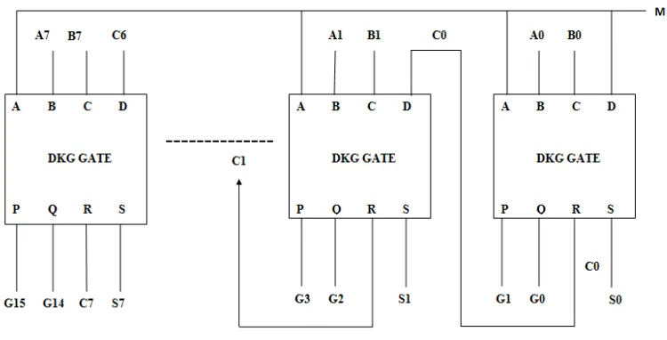
III. PROPOSED WORK A. Design 1: 8-Bit Adder-Subtractor Using DKG Gates
In this approach DKG gates are used for adder Subtractor design. As shown in figure 7, the design has a total of 8 DKG gates cascaded to work as 8-bit adder-subtractor.the Binary numbers A and B are applied to the second and third inputs of DKG gate whereas as first input is connected to mode and fourth input is also connected to mode for first gate whereas for all other gates is connected to previous carry. This design approach generates a total of 16 garbage outputs. Quantum cost of this design is 48. The expression for adder and subtractor is given below [13]:
Sum=A⊕B⊕CIN
Carry= (A⊕B) CIN⊕AB
Difference=A⊕B⊕CIN
Borrow=A’B+BCIN+CINA’
[image:4.612.117.492.412.603.2]Where CIN is the previous carry in case of adder and previous borrow in case of subtractor [8].
Fig. 7 Proposed design for reversible 8-bit adder-subtractor using DKG gate
B. Design 2: 16-Bit Adder Subtractor using WG Gates
Fig. 8 Proposed design for reversible 16-bit adder-subtractor using WG gate
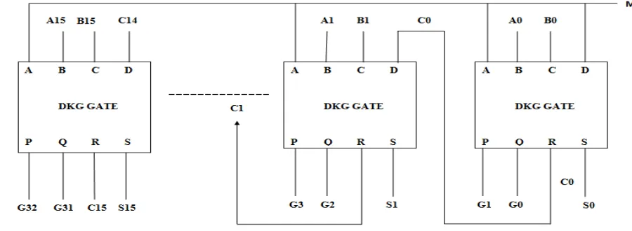
C. Design 3: 16-Bit Adder Subtractor using DKG Gates
[image:5.612.93.532.94.257.2]The design has a total of 16 DKG gates cascaded to work as 16-bit adder-subtractor. This design approach generates a total of 32 garbage outputs. Quantum cost of this design is 96.
Fig. 9 Proposed design for reversible 16-bit adder-subtractor using DKG gate
IV. IMPLEMENTATION AND RESULTS A. Design 1
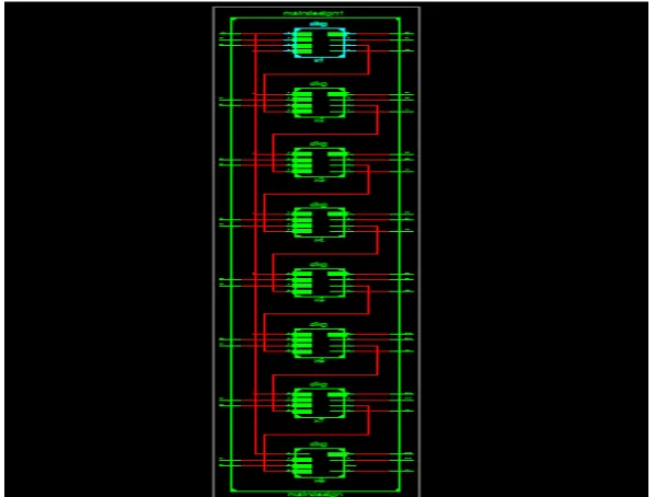
[image:5.612.72.522.346.511.2]Fig. 11 RTL view of synthesized 8-bit adder-subtractor using DKG gates
Fig. 12 Power Consumption for reversible 8-bit adder-subtractor using DKG gate
[image:6.612.32.556.521.699.2]Fig. 14 Comparative results of power consumption graph for proposed and existing design.
[image:7.612.147.467.311.538.2]B. Design 2
[image:7.612.62.564.573.716.2]Fig. 15 Proposed design of 16-bit Adder-Subtractor circuit using WG gates
C. Design 3
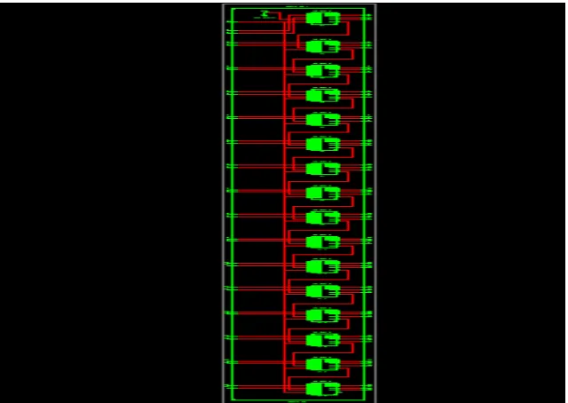
[image:8.612.56.554.349.503.2]Fig. 17 Proposed design of 16-bit adder-subtractor using DKG gate
Fig. 18 Power Consumption for reversible 16-bit adder-subtractor using DKG gate
[image:8.612.46.543.548.701.2]Table 1: Comparison of proposed work with existing work. Sr.
No.
Parameters 8 bit adder-subtractor design 16 bit adder-subtractor design
Proposed Existing [16] Proposed Proposed
1. Quantum cost 48 56 112 96
2. Power consumption(W) 0.091 3.643 4.436 1.983
V. CONCLUSION
Reversible logic is an emerging technology which will lead to lesser power consumption and no power loss. In this paper 8-bit and 16-bit adder-subtractor circuits are designed using WG gate and DKG gate. Table 1 demonstrates that proposed design is better than existing design in terms of quantum cost and power consumption. The quantum cost of 8-bit adder-subtractor design using DKG gate is 48 and its power consumption is 0.091W whereas the quantum cost of existing design is 56 and its power consumption is 3.643W, the quantum cost of 16-bit adder-subtractor using WG gate is 112 and its power consumption is 4.436W, quantum cost of 16-bit adder-subtractor using DKG gate is 96 and its power consumption is 1.983W. Hence the proposed circuit is better than existing circuit in terms of quantum cost and power consumption.
REFERENCES
[1] Rolf Landauer, “Irreversibility and Heat Generation in the Computational Process,” IBM Journal of Research and Development, 5, pp. 183-191, 1961. [2] C H Bennett, “Logical Reversibility of Computation,” IBM J.Research and Development, pp. 525-532, November 1973.
[3] Hafiz Md. Hasan Babu, Md. Rafiqul Islam, Syed Mostahed Ali Chowdhury, Ahsan Raja Chowdhury, “Synthesis of Full-Adder Circuit Using Reversible Logic,” VLSI Design, 2004. Proceedings. 17th International Conference on. IEEE, 2004.
[4] Prashant .R.Yelekar, Prof. Sujata S. Chiwande, “Introduction to Reversible Logic Gates & its Application,” 2nd National Conference on Information and Communication Technology (NCICT) 2011.
[5] Himanshu,Thapliyal and Nagarajan Ranganathan, "Design of efficient reversible binary subtractors based on a new reversible gate," VLSI, 2009. ISVLSI'09. IEEE Computer Society Annual Symposium, IEEE, 2009.
[6] Maii T.Emam, and Layle A A Elsayed, "Reversible Full Adder/Subtractor,” Symbolic and Numerical Methods, Modeling and Applications to Circuit Design (SM2ACD), 2010 XIth International Workshop on. IEEE, 2010
[7] Himanshu Thapliyal and Nagarajan Ranganathan , "A new reversible design of BCD adder," Design, Automation & Test in Europe Conference & Exhibition, IEEE, 2011.
[8] Parminder Kaur, Balwinder Singh Dhaliwal, "Design of fault tolearnt full adder/subtarctor using reversible gates,” Computer Communication and Informatics (ICCCI), 2012 International Conference on. IEEE, 2012.
[9] Raghava Garipelly, P.Madhu Kiran, A.Santhosh Kumar ‟A Review on Reversible logic gates and their Implemantation”, International journal of emerging and advanced engineering, March2013, volume3, Issue3.
[10] Ankur Sarker, Avishek Bose, Shalini Gupta, "Design of a compact fault tolerant adder/subtractor circuits using parity preserving reversible gates," Computer and Information Technology (ICCIT), 2014 17th International Conference on. IEEE, 2014.
[11] Papiya Biswas, Namit Gupta, Nilesh Patidar,” Basic Reversible Logic Gates and It’s Qca Implementation,” Int Journal of Engineering Research and Applications ISSN : 2248-9622, Vol. 4, Issue 6( Version 5), June 2014, pp.12-16.
[12] A. N. Nagamani, S. Ashwin, Vinod Kumar Agrawal, "Design of optimized reversible binary adder/subtractor and BCD adder," Contemporary Computing and Informatics (IC3I), 2014 International Conference on. IEEE, 2014
[13] K. Prasad Babu, S.Ahmed Basha, M.Chenniah, H.Devanna, "Design of low power FULLADDER using NG and NTG gates," Smart Structures and Systems (ICSSS), 2014 International Conference on. IEEE, 2014.
[14] Lenin Gopal, Adib Kabir Chaudhary, Alpha Agape Gopalai, Ashutosh Kumar Singh, Bakri Madon, "Reversible logic gate implementation as switch controlled reversible full adder/subtractor," Control System, Computing and Engineering (ICCSCE), 2014 IEEE International Conference on. IEEE, 2014.
[15] M.Aditya, YB Nithin Kumar, M. H. Vasantha, "Reversible full/half adder with optimum power dissipation,” Intelligent Systems and Control (ISCO), 2016 10th International Conference on. IEEE, 2016
[16] Vandana Shukla, O. P. Singh, G. R. Mishra, R. K. Tiwari, “A Novel Approach for Reversible Realization of 8-Bit Adder-Subtractor Circuit with Optimized Quantum Cost,” in IEEE ISBN 978-1-4673-6725-7,2016.
[17] Ankush, Amandeep Singh Bhandari, “Review Paper on Reversible Logic Gate”, International Journal for Research in Electronics & Communication Engineering, vol. 1, Issue 7, (2016).
[18] Ankush, Amandeep Singh Bhandari, “Design & Performance Analysis of Low Power Reversible Carry Skip Adder”, IOSR Journal of VLSI and Signal Processing, vol. 6, Issue 4, Ver. II,(2016),pp.33-39
[19] Ankush, Amandeep Singh Bhandari, “Design & Performance Analysis of Low Power Reversible Residue Adder”, International Journal of Hybrid Information Technology, vol. 9,Issue 9,(2016),pp.93-102.
[20] Amandeep Singh Bhandari and Priya Sharma, “Introduction to Reversible Logic and Mathematical Derivation for V and V+ Gates”, International Journal of Computer Applications (0975 – 8887) Volume 153 – No5, November 2016, pp 14-18.
![Fig. 1 N*N Reversible logic gate symbol [10]](https://thumb-us.123doks.com/thumbv2/123dok_us/8307302.856641/2.612.228.367.420.505/fig-n-n-reversible-logic-gate-symbol.webp)
![Fig. 3 Double Feynman Gate [4]](https://thumb-us.123doks.com/thumbv2/123dok_us/8307302.856641/3.612.237.396.338.394/fig-double-feynman-gate.webp)