PARIS RESEARCH LABORATORY
d i g i t a l
June 1989
3
3
Introduction to
Programmable Active Memories
Patrice Bertin Didier Roncin
Jean Vuillemin
Publication Notes
An earlier version of this report appears, with the same title, in Systolic Array Processors, edited by J. McCanny, J. McWhirter, and E. Swartzlander Jr. and published by Prentice Hall, 1989.
Patrice Bertin is a member of the Institut National de Recherche en Informatique et Automa-tique, Rocquencourt, 78150 Le Chesnay, France, on a research contract at Digital Equipment Corporation, Paris Research Laboratory.
c
Digital Equipment Corporation 1993
This work may not be copied or reproduced in whole or in part for any commercial purpose. Permission to copy in whole or in part without payment of fee is granted for non-profit educational and research purposes provided that all such whole or partial copies include the following: a notice that such copying is by permission of the Paris Research Laboratory of Digital Equipment Centre Technique Europe, in Rueil-Malmaison, France; an acknowledgement of the authors and individual contributors to the work; and all applicable portions of the copyright notice. Copying, reproducing, or republishing for any other purpose shall require a license with payment of fee to the Paris Research Laboratory. All rights reserved.
Abstract
We introduce the concept of PAM, Programmable Active Memory and present results obtained with our Perle-0 prototype board, featuring:
A software silicon foundry for a 50K gate array, with a 50 milliseconds turn-around
time.
A 3000 one bit processors universal machine with an arbitrary interconnect structure
specified by 400K bits of nano-code.
A programmable hardware co-processor with an initial library including: a long
multiplier, an image convolver, a data compressor, etc. Each of these hardware designs speeds up the corresponding software application by at least an order of magnitude.
R ´esum ´e
Nous pr´esentons le concept de m´emoire active programmable (PAM) et d´ecrivons diverses exp´eriences et mesures faites sur notre prototype Perle-0 qui est :
Une fonderie logicielle de silicium, pour pr´ediffus´es de 50K portes, dont le temps de
rotation est de 50 millisecondes.
Une machine universelle comportant 3000 processeurs un bit. La structure de connexion
entre les processeurs est arbitraire et sa programmation sp´ecifi´ee par 400K bits de nano-code.
Un co-processeur mat´eriel programmable dont la biblioth`eque initiale comprend : un
multiplicateur 512 bits, un convolueur d’images noir et blanc, un compresseur de donn´ees, etc. Chacune de ces configurations acc´el`ere l’application logicielle correspon-dante de plus d’un ordre de grandeur.
Keywords
programmable hardware co-processor, programmable gate array, bit-level algorithms, long multiplier, data compression, image convolution.
Contents
1 Concept 1
2 Implementation 2
3 PAM programming 3
4 Design experiments 4
4.1 Early experiments : : : : : : : : : : : : : : : : : : : : : : : : : : : : : 4
4.2 Long multiplication : : : : : : : : : : : : : : : : : : : : : : : : : : : : : 5
4.3 Data compression : : : : : : : : : : : : : : : : : : : : : : : : : : : : : 6
4.4 Image processing : : : : : : : : : : : : : : : : : : : : : : : : : : : : : 6
5 Conclusion 6
References 8
Introduction to Programmable Active Memories 1
1 Concept
Definition (Programmable Active Memory: PAM)
A PAM is a uniform array of identical cells all connected in the same repetitive fashion. Each cell, called a PAB for programmable active bit, must be general enough so that the following holds true: Any synchronous digital circuit can be realized (through suitable programming) on a large enough PAM for a slow enough clock.
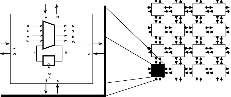
[image:9.612.81.484.199.368.2]n s e w r N S E W R cl k n N E e w W S s
Figure 1: A simple PAM
Figure 1 shows a simple PAM implementation as a regular matrix of Manhattan connected identical PABs. Each PAB has:
4 inputs<n;s;e;w>;
4 outputs<N;S;E;W>;
1 register (flip-flop) with input R and output r, synchronous with the PAM’s global clock
clk;
1 combinatorial gate g connected so that: g(n;s;e;w;r) =<N;S;E;W;R>;
160=532control bits which specify the truth table of function g.
A program for such a PAM with m active bits is a sequence of160m control bits (bitstream) representing the truth tables for each PAB. This program can be downloaded into the control part of the PAM. From this instant, and until the program is changed again, our PAM behaves as the particular finite state machine specified by the bitstream.
Other PAM implementations are possible:
2 Patrice Bertin, Didier Roncin, and Jean Vuillemin
the Configurable Array Logic (CAL) reported in [3] is close to the one above;
the Logic Cell Array (LCA) is a cMOS component designed by Xilinx Inc. [7]. Except
for minor details, it is similar to the above description with each of our<n;s;e;w>and
<N;S;E;W>variables carrying 4 signals instead of one. The truth table of function g
is reduced, for obvious practical reasons: only one general 5 input boolean function is actually specified; the remaining part of g is used to specify various switchboxes, usable to route the signals.
Our investigation aims at answering the following questions:
How to build large PAMs?
How fast can it run?
Which class of design can we efficiently map onto a PAM?
How do we implement PAM designs?
2 Implementation
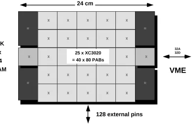
Using a 55 array of LCA chips, we have built a4080 ' 3K bit PAM named Perle-0
on a2525cm
2printed circuit board. Perle-0 has a VME bus interface, which makes it a
general-purpose configurable hardware co-processor tightly coupled to a host CPU (Figure 3).
The configuration data for Perle-0 (about 400K bits) is downloaded by the host itself in 50 milliseconds. The logic controlling the download process, as well as the host bus communication protocol are programmed into two extra LCAs, statically configured at power-up time from a PROM. By merely changing the content of that PROM, we are able to quickly adapt to different bus protocols, or to add extra features to the bus interface.
The PAM cycle being much faster than that of the host bus, we added 4 Megabits of fast static RAM to Perle-0, directly connected to the PAM (the bandwidth of that memory is up to 1.5 Gigabits per second, while the host bus bandwidth is typically around 50 Megabits per second). Besides a few mandatory buffers for driving the host bus, Perle-0 is thus built out of two kinds of components: LCA and static RAM (Figure 2).
PAM designs are synchronous logic circuits, each of the registers being updated on each cycle of a global clock signal. The maximal clock speed for such a design is directly determined by its critical combinatorial path, which varies from one design to another. It has thus been necessary to design a clock distribution system whose speed can be programmed as part of the design configuration, for speeds up to 70 MHz (the present maximum clock cycle of LCA chips).
Last but not least, we take advantage of an extra feature of the LCA component which makes it possible to dynamically read back the content of each PAB. Together with a “software
Introduction to Programmable Active Memories 3
R
R X
X X X X X
X X X X X
X X X X X
X X X X X
X X X X X
R
R X
24 cm
25 x XC3020 = 40 x 80 PABs
64K x 64
RAM
VME
128 external pins
[image:11.612.107.498.92.353.2]32A 32D
Figure 2: Perle-0
stepping” facility (stop the main clock and trigger clock cycles one at a time from the host) this provides a powerful debugging tool which can take a snapshot of the internal state of the design after each clock cycle.
3 PAM programming
The logical description of a PAM design consists of the truth table for each PAB and the description of their interconnection. In order to derive the final configuration bitstream for each LCA, we also need to specify the placement of each block within the PAM, as well as the actual routing of each signal through the available channels and switching boxes.
At the LCA level, both placement and routing may be automatically generated by Xilinx software. We have found this to be practical only for routing; automatic placement is far too time-consuming and it generally yields poor results: in this technology, each programmable interconnection point adds about 2 nanoseconds to the signal propagation delay. Therefore, a poor relative block placement may considerably affect the final design performance.
In our CAD system, the designer needs to specify the logic equations and net names for each PAB; optionally he may also control the actual placement of each PAB. This is achieved through a program in a high-level language (we use Modula-2+ and Lisp) or through schematic
4 Patrice Bertin, Didier Roncin, and Jean Vuillemin
entries. Netlists are then generated for each of the 25 LCAs of Perle-0 and we use Xilinx software to finish the placement, do the actual routing and produce the bitstream for each LCA. Finally, the 25 bitstreams are merged into a 400K bits long file ready to be downloaded by the host into the PAM.
The above steps typically take from 15 minutes to a few hours, depending on the complexity of the design; subsequent minor modifications are generally much faster. The actual downloading is then performed in 50 ms. Since debugging the designs can be done through stepping and readback, this effectively brings hardware design times very close to these of software. In particular, it provides a vehicule for experimenting with hardware algorithms which would otherwise be too time-consuming and costly to implement.
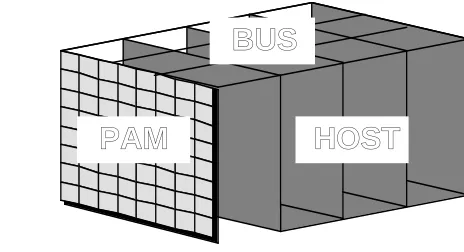
HOST
BUS
PAM
• Programmed Host Bus
Interface.
• Configuration from Host
in 50 ms.
• Design loop from 2mn to
2hrs.
• Dynamic Read Back for
[image:12.612.282.514.262.388.2]Active Bits.
Figure 3: Perle-0 setup
4 Design experiments
We describe here some of the designs which have been successfully tested on Perle-0. More designs are currently in progress.
4.1 Early experiments
Our first designs aim at debugging and testing the performance of Perle-0 itself:
A software-controlled variable clock generator, used as a basic block in building other
designs.
A combinatorial link established through all the pins, in order to test the printed
circuit board traces for electrical continuity; it also implements one of the worst-case combinatorial delay achievable through routing, and runs at 4 MHz.
Introduction to Programmable Active Memories 5
A 3K shift-register through all of the PAM’s active bits. It provides an example of the
fastest possible synchronous design and proves operational at clock speeds up to 50 MHz.
Designs to read and write Perle-0’s RAM from the host. Their speed is limited by the
VME bus bandwidth, at about 50 Mbits/s.
Such simple designs typically take a few hours to build, compile and debug.
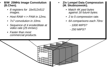
• B/W 25MHz Image Convolution (B.Chen).
• 8 registers for 1bx512x512 images.
• Host RAM <-> PAM in 12ms. • 7x7 convolution in 10ms. • Sequence of 4 erode/dilate at
video rate (25 im/sec).
• Faster than most
commercial products.
• Ziv Lempel Data Compression (M. Skubiszewski).
• Match 4K past bytes against 16 future bytes. • 2 to 5 compression rate. • 64 comparisons each 70ns:
- 1000 MIPS? - 250 MIPS?
[image:13.612.85.492.196.456.2]PAM
Figure 4: Two PAM designs
4.2 Long multiplication
We have programmed Perle-0 into a fast 512-bit multiplier (see [4]) computing
P=AB + S where:
- A is a m bit integer, with m512;
- B is a n bit integer, with n>0arbitrary;
- S is a n + m bit integer;
- P is a n + m +1bit integer.
6 Patrice Bertin, Didier Roncin, and Jean Vuillemin
The host writes the A, B and S operands into the PAM, and reads back the resulting P. The speed-up factor achieved by this hardware co-processor can be greater than 25 for long operands, compared to carefully hand-coded software. It computes a 1K bit product in 210 microseconds, which makes this PAM design faster than any known machine for which we could obtain benchmark measures. It is 4 times faster than a Cyber 170/750.
The multiplier is interfaced with an arbitrary-precision arithmetic package [6] so that any program based on that software takes advantage of the PAM without modification. For example, Hans Boehm has run computations for exact real arithmetic [1] with typical speedups from 3 to 7. We have written code for modular products and used it for RSA cryptography [5]. The PAM computes RSA encryption/decryption at 3900 bits per second for arbitrary 512-bit keys; this is about 4.5 times faster than our best software version on the same host.
The first operational version of the multiplier was developed in less than a week. Two subsequent versions, which refined the design on the basis of actual performance measurements, were each developed in less than 5 man-days.
4.3 Data compression
A hardware accelerator for data compression was implemented in four months by Marcin Skubiszewski, who had no previous hardware experience. Based on an algorithm described in [2], it is a massively parallel method (64 byte comparisons each 70 ns), which repetitively matches the next 16 bytes in the file to be compressed against the last 4k bytes seen (stored in the local RAM) in order to detect the longest substring previously seen (see [8]). The resulting design achieves an average compression ratio varying from 2 for English text to 3 for source code.
4.4 Image processing
J. Bradley Chen has implemented the operations of erosion and dilation (two-dimensional boolean convolution) on5125121-bit images, with77-bit masks. The design runs at
25 MHz, computing one bit of the transformed image on each cycle, for a total of 10 ms per image. Our best software solution for that problem is at least two orders of magnitude slower. This design was implemented in about 3 months of work, once again with minimal previous hardware experience.
5 Conclusion
PAM is an exciting new technology, with a lot of growth potential. Based on our first year of experiments, we derive the following conclusions:
Prototyping. While custom hardware prototyping times are at best measured in months,
prototyping with PAM is achieved in weeks. Design times for PAM must be compared
Introduction to Programmable Active Memories 7
with those of software, not of hardware.
Speed. Assuming equal technology, custom hardware designs are faster than their PAM
implementation; yet the speed loss appears to be less than 50% for systolic designs with short connections.
Size. While custom hardware designs are obviously smaller than their PAM counterpart, the
same PAM can be used to run any number of hardware designs! We regard the PAM as a hardware cache: it can be programmed to perform arbitrary tasks, at speeds comparable to those of custom hardware.
Size vs. Speed. All our designs are such that we can double the bandwidth on a twice bigger
PAM. This provides a strong incentive to build much larger ones.
Architecture. As a general purpose computing device, Perle-0 exhibits some unique features:
The bitstream is a program for Perle-0 which is thus the ultimate one-instruction
RISC machine (400K wide nano-code!).
The PAM is a parallel machine with 3000 one-bit processors. The interconnect
structure between these processors can be arbitrary, since it is specified by the program. Exotic interconnect structures (hypercube and such) are feasible, but they use up more PAM area and run with slower clocks.
The host and PAM system is a silicon foundry with a 50 ms turn-around time. The
host can also read back the content of each active bit in the PAM, providing an invaluable design independent debugging tool.
The PAM is a flexible structure which can be tailored (logic, memory and
interconnect) to the efficient implementation of any well designed massively parallel bit-level algorithm. This should be contrasted with the usual situation where the algorithm must be chosen so as to adapt to the structure of the implementation machine.
8 Patrice Bertin, Didier Roncin, and Jean Vuillemin
References
1. Boehm, H. J. Constructive real interpretation of numerical programs. In Proceedings of the ACM Conference on Interpretors (1987) 214–221.
2. Fiala, E. R. and Greene, D. H. Data compression with finite windows. Communications of the ACM, 32, 4 (April 1989) 490–505.
3. Kean, T. and Gray, J. Configurable hardware: two case studies of micro-grain computation. In McCanny, J., McWhirter, J., and Swartzlander Jr., E., editors, Systolic Array Processors, Prentice Hall (1989) 310–319.
4. Lyon, R. F. Two’s complement pipeline multipliers. IEEE Transaction on Communications, 24 (1976) 418–425.
5. Rivest, R. L., Shamir, A., and Adleman, L. A method for obtaining digital signatures and public-key cryptography. Communications of the ACM, 21, 2 (February 1978) 120–126.
6. Serpette, B., Vuillemin, J., and Herv´e, J.C. BigNum: A Portable and Efficient Package for Arbitrary-Precision Arithmetic. Research Report No. 2, Digital Equipment Corp., Paris Research Laboratory, Rueil-Malmaison (1989).
7. Xilinx, Inc. The Programmable Gate Array Data Book. (1988). Product Specifications.
8. Ziv, J. and Lempel, A. A universal algorithm for sequential data compression. IEEE Transactions on Information Theory, 23, 3 (March 1977) 337–343.
PRL Research Reports
The following documents may be ordered by regular mail from: Librarian – Research Reports
Digital Equipment Corporation Paris Research Laboratory 85, avenue Victor Hugo 92563 Rueil-Malmaison Cedex France.
It is also possible to obtain them by electronic mail. For more information, send a message whose subject line [email protected], from within Digital, todecprl::doc-server.
Research Report 1: Incremental Computation of Planar Maps. Michel Gangnet, Jean-Claude Herv ´e, Thierry Pudet, and Jean-Manuel Van Thong. May 1989.
Research Report 2: BigNum: A Portable and Efficient Package for Arbitrary-Precision Arithmetic. Bernard Serpette, Jean Vuillemin, and Jean-Claude Herv´e. May 1989.
Research Report 3: Introduction to Programmable Active Memories. Patrice Bertin, Didier Roncin, and Jean Vuillemin. June 1989.
Research Report 4: Compiling Pattern Matching by Term Decomposition. Laurence Puel and Asc ´ander Su ´arez. January 1990.
Research Report 5: The WAM: A (Real) Tutorial. Hassan A¨ıt-Kaci. January 1990.y
Research Report 6: Binary Periodic Synchronizing Sequences. Marcin Skubiszewski. May 1991.
Research Report 7: The Siphon: Managing Distant Replicated Repositories. Francis J. Prusker and Edward P. Wobber. May 1991.
Research Report 8: Constructive Logics. Part I: A Tutorial on Proof Systems and Typed
-Calculi. Jean Gallier. May 1991.
Research Report 9: Constructive Logics. Part II: Linear Logic and Proof Nets. Jean Gallier. May 1991.
Research Report 10: Pattern Matching in Order-Sorted Languages. Delia Kesner. May 1991.
y
This report is no longer available from PRL. A revised version has now appeared as a book: “Hassan A¨ıt-Kaci,
Research Report 11: Towards a Meaning of LIFE. Hassan A¨ıt-Kaci and Andreas Podelski. June 1991 (Revised, October 1992).
Research Report 12: Residuation and Guarded Rules for Constraint Logic Programming. Gert Smolka. June 1991.
Research Report 13: Functions as Passive Constraints in LIFE. Hassan A¨ıt-Kaci and Andreas Podelski. June 1991 (Revised, November 1992).
Research Report 14: Automatic Motion Planning for Complex Articulated Bodies. J ´er ˆome Barraquand. June 1991.
Research Report 15: A Hardware Implementation of Pure Esterel. G ´erard Berry. July 1991.
Research Report 16: Contribution `a la R ´esolution Num ´erique des ´Equations de Laplace et de la Chaleur. Jean Vuillemin. February 1992.
Research Report 17: Inferring Graphical Constraints with Rockit. Solange Karsenty, James A. Landay, and Chris Weikart. March 1992.
Research Report 18: Abstract Interpretation by Dynamic Partitioning. Fran¸cois Bourdoncle. March 1992.
Research Report 19: Measuring System Performance with Reprogrammable Hardware. Mark Shand. August 1992.
Research Report 20: A Feature Constraint System for Logic Programming with Entailment. Hassan A¨ıt-Kaci, Andreas Podelski, and Gert Smolka. November 1992.
Research Report 21: The Genericity Theorem and the Notion of Parametricity in the Poly-morphic -calculus. Giuseppe Longo, Kathleen Milsted, and Sergei Soloviev. December
1992.
Research Report 22: S ´emantiques des langages imp´eratifs d’ordre sup ´erieur et interpr ´etation abstraite. Fran¸cois Bourdoncle. January 1993.
Research Report 23: Dessin `a main lev ´ee et courbes de B ´ezier : comparaison des al-gorithmes de subdivision, mod´elisation des ´epaisseurs variables. Thierry Pudet. January 1993.
Research Report 24: Programmable Active Memories: a Performance Assessment. Patrice Bertin, Didier Roncin, and Jean Vuillemin. March 1993.
Research Report 25: On Circuits and Numbers. Jean Vuillemin. April 1993.
Research Report 26: Numerical Valuation of High Dimensional Multivariate European Secu-rities. J ´er ˆome Barraquand. March 1993.
Research Report 28: Feature Automata and Sets of Feature Trees. Joachim Niehren and Andreas Podelski. March 1993.
Research Report 29: Real Time Fitting of Pressure Brushstrokes. Thierry Pudet. March 1993.
Research Report 30: Rollit: An Application Builder. Solange Karsenty and Chris Weikart. April 1993.
Research Report 31: Label-Selective-Calculus. Hassan A¨ıt-Kaci and Jacques Garrigue.
May 1993.
Research Report 32: Order-Sorted Feature Theory Unification. Hassan A¨ıt-Kaci, Andreas Podelski, and Seth Copen Goldstein. May 1993.
Research Report 33: Path Planning through Variational Dynamic Programming. J ´er ˆome Barraquand and Pierre Ferbach. September 1993.
Research Report 34: A penalty function method for constrained motion planning. Pierre Ferbach and J ´er ˆome Barraquand. September 1993.
Research Report 35: The Typed Polymorphic Label-Selective-Calculus. Jacques Garrigue
3
In
tr
oduc
tion
to
Progra
mma
bl
e
A
c
tiv
e
M
e
m
ori
e
s
P a tr ic e B er tin, Didier Ronc in, and J ean V u illem ind i g i t a l
PARIS RESEARCH LABORATORY 85, Avenue Victor Hugo