Design of Encryption System using NIOS II Processor
Madhav M. Deshpande
Research Scholar, R.C.O.E.M, NagpurMeghana A. Hasamnis
Associate Professor, Electronics Department R.C.O.E.M, Nagpur
ABSTRACT
The use of embedded systems in various applications has increased extensively over last few years. Embedded systems allow hardware & software go hand in hand to perform some specific task. As the application demand goes on increasing with the time the complexity of the embedded system increases. At the same time, the size of integrated circuits should be limited considering the basic criteria for embedded system like, quality of system, quantity of system, speed of system, Performance of system and Power consumption of system. While designing system according to this criterion complexity of the system increases. To reduce complexity of system, it is designed using balanced hardware & software flow of design. This combined design of hardware & software is known as Co-Design. Using this approach we build dedicated software and hardware units on the single chip i.e. SoC design.
KEYWORDS
Co-Design, image processing, DCT(Discrete cosine transform), Custom instruction.
1.
INTRODUCTION
In last few decades, embedded systems have experienced an accelerating growth both in computing power and scope of their possible applications. Moreover the designing procedure for embedded system also changed immensely. As the application demands goes on increasing with the time the complexity of the embedded system is waxing. Combination of software and hardware in design leads to improve the system performance such approach is known as Co-Design.
1.1 CO-DESIGN
Hardware/software co-design is the main technique used in the thesis. It can be defined as the cooperative design of hardware and software. The aim of co-design is to abridge the time-to-market while reducing the design effort and costs of the designed products [1].
Co-design can be implemented on embedded systems and processor is the main part of any embedded system. As software is more flexible and cheaper than hardware, the advantage of using processors is multiple. This suppleness of software allows late design changes and verified debugging opportunities. Moreover, the possibility of reusing software by porting it to other processors reduces the time-to market and the design effort. [1][4].hardware is always used in design, when processors are not able to meet the required performance. This exchange between hardware and software illustrates the optimization aspect of the co-design problem.
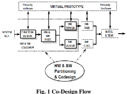
[image:1.595.319.537.233.393.2]Co-design is an interdisciplinary activity, bringing concepts and ideas from diverse disciplines together, e.g. system-level modeling, hardware design and software design [3].
Fig. 1 Co-Design Flow
The design flow of the general co-design approach is depicted in figure 1
Step1: The co-design process starts with specifying the system behavior at the system level.
Step 2: After this, a pure software system will be developed to verify all algorithms.
Step 3: Performance analysis will be performed to find out the system bottlenecks.
Step 4: The hardware/software partitioning phase a plan will be made to determine which parts will realized by hardware and which parts will be realized by software. Obviously, some system bottlenecks will be replaced by hardware to improve the performance.
Step 5: based on the results of step 4, hardware and software parts will be designed respectively.
Step 6: co-simulation. At this step, the completed hardware and software parts will be integrated together and performance analysis will be performed.
Step 7: if the performance meets the requirements, the design can stop and if the
Performance can’t meet the requirements, new HW/SW partitioning and a new design.
1.2 Motivation
continual verification throughout the design cycle, mutual influence of both HW and SW early in the design cycle, partitioning (Co-design) is the only way to get all this features [3].
The advanced ASIC and FPGA technologies facilitate the integration of complex Systems on a Chip (SoC). The use of different Co-design methods is application specific. In our project work we required an opaque and fast system. The Nios II soft-core processor have the highest operating frequency for FPGA implementation, it also allows reuse of code and highly configurable [14]. These esteem features motivated to select AES Algorithm for implementation using Co-design with NIOS II soft core processor and study the performance parameters.
1.3 Aim and Objective
The objective of our paper is
1. Implementation of AES algorithm on Cyclone II FPGA using NIOS II Processor.
2. Implementation of AES algorithm on Cyclone II FPGA using NIOS II Processor with Custom Instruction
3. Comparison of algorithm in terms of speed and area for both the designs of AES algorithm (Encryption) with and without custom instruction
2.
RIJNDAEL ENCRYPTION
ALGORITHM
[image:2.595.374.521.118.241.2]The algorithm originates from the initiative of the National Institute of Standards and Technology (NIST) in 1997 to select a new symmetric key encryption algorithm. Rijndael algorithm was selected as the Advanced Encryption Standard (AES) because of its security, performance, efficiency, ease of implementation and flexibility. The algorithm includes three main parts: Cipher, Inverse Cipher and Key Expansion. Cipher converts data to a jumbled form called cipher text while Inverse Cipher converts data back into its original form called plaintext. Key Schedule is generated by Key Expansion that is used in Cipher and Inverse Cipher procedure. There are Specific number of rounds required to generate cipher and Inverse Cipher (Table 1). For the AES algorithm, the number of rounds to be performed during the execution of the algorithm is dependent on the key length.
Table 1.
Block size Nb
words
Key length Nk
words
No. of rounds Nr
AES-128 bit key 4 4 10
AES-192 bit key 4 6 12
AES-256 bit key 4 8 14
2.1
Encryption Process
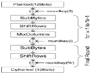
The Encryption process of Advanced Encryption Standard algorithm is given below,
[image:2.595.70.290.609.720.2]
Figure 2 Encryption Process
In Encryption process, each round consists of four operations: SubBytes, ShiftRows, MixColumns and AddRoundkey. For 128 bit key, there will be total 10 rounds. But in last round there will be no Addrounkey operation.
SubBytes: The input data and key is given in the form of a matrix. Data entry in each matrix is of a byte size. The X-or operation is performed between data and key to make new matrix. Each byte in the matrix is replaced by the byte from S-box, where S-box is a standard substitution table in algorithm.
ShiftRows: After Subbyte process the bytes in matrix are shifted to lest side. First row of matrix is remain unchanged, second row is shifted left by 1 byte, third row by by 2 bytes and final row is shifted by 3 bytes to form new matrix.
MixColumns: This transformation is based on Galois Field multiplication. Each byte of a column is changed with another value that is a function of all four bytes in the given column. The MixColumn transformation executes on the State column-by-column, treating each column as a four-term polynomial GF (28).
Addroundkey: In the Addition of Round Key transformation, a Round Key is added to the State matrix by a simple bitwise X-OR operation done on plain text and input key. Each Round Key consists of Nb words from the key schedule generation. Those Nb words are each added into the columns of the State
3. Implementation of Algorithm on FPGA using
NIOS II Processor
AES Algorithm will be implemented on CYCLON II FPGA using NIOS II Processor and the software used are Quartus II and NIOS II IDE.
NIOS II is a synthesizable VHDL model of a 32-bit processor compliant with the SPARC V8 architecture. The processor is highly flexible in any design configuration, and mainly suitable for system-on-a-chip (SOC) designs. The NIOS II IDE have GNU compiler with C/C++ license, Following are some features of NIOS II Soft core Processor.
Reduced Instruction Set Computer (RISC)8/16/32-bits memory controller for external PROM and SRAM
No pipeline, 5 or 6 stages pipeline configurations
It has full 32-bit instruction set
32 general-purpose registers
For more interrupt sources it has external interrupt controller interface
Single-instruction 32 × 32 multiply and divide producing a 32-bit result
For computing 64-bit and 128-bit products dedicated instructions of multiplication is given
Floating-point Custom instructions for single-precision floating-point operations
3.1 Design steps for Implementation
The system components required for Software/Hardware implementation of Encryption or Decryption on FPGA in QUARTUS II software are,
NIOS II Processor
JTAG UART
SRAM MEMORY
Input ,Output GPIO’S
Performance Counter
SOPC Builder automatically generates the interconnect logic to integrate the components in the hardware system. It can be selected from a list of standard processor cores and components provided with the Nios II EDS [14].
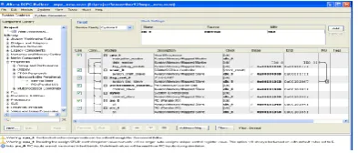
[image:3.595.324.534.70.161.2]Following window shows the selection of components required and its system generation
Figure 3 System contents in SOPC Builder
[image:3.595.321.533.252.331.2]In the Figure 3, the components required to build a system are taken in SOPC Builder.
Figure 4 System Generation without custom instruction
[image:3.595.70.267.402.486.2]In Figure 4, the successful generation of the system is shown.
Figure 5 NIOS System without custom instruction Block Diagram File view
[image:3.595.60.273.544.624.2]In Figure 5, integration of SOPC Builder with Quartus Software is shown. In this BDF the pin assignment is done by importing the pin assignment of Cyclone II (EP2C35F672C6) FPGA.
Figure 6 Hardware Generation of System in Cyclone II (EP2C35F672C6) FPGA
In Figure 6, the generation of system in hardware is shown. Here the connection between Cyclone II FPGA and host computer is done by cable USB-Blaster. After successful hardware generation time limited file is generated.
3.1.2 Results for AES using NIOS II System
The results for encryption using NIOS II IDE with 128-bit key and 128 bit plaintext/cipher text written in c-code has given below.
After Generation of system in Quartus II software the .sopcinfo file is called up in NIOS II IDE as a hardware platform. The new project is made in NIOS II IDE, then the project for C-code is chosen in which the “hello_world” template is selected.
The C-code for AES Algorithm are written in Hello_world.c file (Encryption & Decryption separately). Then the project is build using Build Project command.
After the project build the code will be implemented on CYCLONE II (EP2C35F672C6) FPGA using command Run as NIOS II Hardware. After all these steps the output will be seen in NIOS II Console Window [18].
[image:3.595.317.541.638.714.2]In Figure 7, the output of implementation of Algorithm (Encryption) on FPGA is shown with clock cycles and time required for execution of Algorithm (Encryption)
Table no. 2 Clock Cycles for execution of Algorithm
4.
Implementation of Algorithm with
custom instruction on FPGA using
NIOS II Processor
In this implementation custom instruction is added in Nios II processor which is used for acceleration in software flow which takes more time. Custom instruction is directly connects to ALU of Nios II processor as a hardware shown in Figure 8
Figure 8 Custom Instruction Logic connects to ALU in
SOPC builder system
4.1 Design steps for Implementation
In Hardware implementation, Custom Instruction is added in NIOS II Processor. The SOPC GUI supports the inclusion of custom instructions.
Figure 9 Inclusion of Custom Instruction in SOPC GUI
Figure 9 shows the addition of custom instruction in NIOS II Processor. The inclusion of Custom Instruction is added as a floating point hardware in processor keeping all other peripherals same, it leads to increase in hardware. The Custom Instruction maps the memory location from SRAM interface in SOPC builder. For data transfer it uses the 32-bit internal registers if Nios II processor [16].
Figure 10 RTL view of Custom Instruction
Figure 10 shows the RTL of Custom Instruction which is of Multicycle type.
4.1.2 Results of AES algorithm using Custom Instruction
The System is generated in SOPC Builder. In this system the custom instruction is added as floating point hardware.
Figure 11 System with Custom Instruction in SOPC Builder
Figure 12 System Generation for Custom Instruction
Figure 11 and Figure 12 shows the system contents and generation of system in SOPC Builder. After generation of system in SOPC, the pin assignment and compilation is done in QUARTUS II.
Figure 13 NIOS System with custom instruction Block Diagram File view
In Quartus II, The pin assignment is done by importing the file of CYCLONE II (EP2C35F672C6) FPGA. In the figure 13 the address lines from SRAM memory are assigned to custom instruction.
Figure 14 RTL view of NIOS II System
Algorithm Clock Cycles Time Required
Figure 14 shows the RTL vies of the system in QUARTUS II. After the successful compilation of system, hardware generation in CYCLONE II FPGA is done and time limited file is generated as shown in Figure 15.
Figure 15 Hardware generation of NIOS II System in CYCLONE II
After hardware generation of system using CYCLONE II FPGA, the algorithm is implemented in NIOS II IDE. We have to follow same steps as stated in chapter 3 with addition of Custom Instruction files in NIOS II IDE Project.
After generating hello_world.c file, we have to add custom instruction files floating_point.c, floating_point.h, floating_point_CI.c and floating_point_SW.c in the project. Then the project is build by command Build Project. While building a project, a macro function system.h is generated which connects the C-code of algorithm to Custom Instruction hardware.
[image:5.595.56.291.403.501.2]After successful build of project the Algorithm is implemented on CYCLONE II (EP2C35F672C6) FPGA. This implementation is done by command Run as NIOS II Hardware. After execution of this command the result is shown in NIOS II console window.
Figure 16 Encryption result with Custom Instruction
In Figure 16, the output of implementation of Algorithm (Encryption) on FPGA is shown with clock cycles and time required for execution of Algorithm (Encryption).
The table no.3 shows the clock cycles required for Encryption and Decryption.
Table no. 3 Clock Cycles for execution of Algorithm
5.
Result and Conclusion
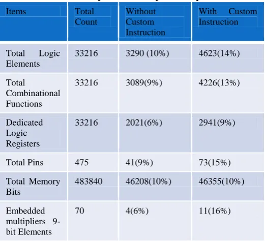
The System generated in SOPC with and without Custom Instruction is compiled in Quartus II environment. The AES algorithm ( Encryption) is compared in terms speed i.e. number of clock cycles required and area in terms of number of Logic elements (LE’s) on FPGA.
5.1 SYNTHESIS REPORT
After execution of Algorithm on FPGA with and without custom instruction, their comparison is done for parameters clock cycles. From the table no. 2 and table no. 3 the comparison is done shown in table no.4
Table 4 CPU Clock cycles and time required
From the performance analysis results of clock cycles and time required for execution of AES algorithm (Encryption)in software i.e. system without Custom Instruction is more as compared with execution of algorithm in hardware i.e. system with custom instruction.
In hardware implementation custom instruction maps the processes in software such as addition, subtraction, multiplication & division directly to the ALU of NIOS II processor which is used directly as hardware. Inclusion of such hardware reduces the clock cycles and time required for execution of algorithm.
The system which is generated using SOPC Builder is compiled in Quartus II software. The hardware required for generation of system is depend upon the LE’s used in CYCLONE II (EP2C35F672C6) FPGA . The comparison in hardware change is shown in table 6.
Table 5 comparison of compilation report
The above table shows the comparison between the software and hardware systems i.e. system with and without custom
Algorithm Clock Cycles Time Required
Encryption 6029854 0.120597 Sec
Items Clock Cycles Time Required
Encryption Without
Custom Instruction
7395826 0.147917 Sec
Encryption With
Custom Instruction
6029854 0.120597 Sec
Items Total
Count
Without Custom Instruction
With Custom Instruction
Total Logic Elements
33216 3290 (10%) 4623(14%)
Total
Combinational Functions
33216 3089(9%) 4226(13%)
Dedicated Logic Registers
33216 2021(6%) 2941(9%)
Total Pins 475 41(9%) 73(15%)
Total Memory Bits
483840 46208(10%) 46355(10%)
Embedded multipliers 9-bit Elements
[image:5.595.299.560.495.732.2]instruction. It shows that inclusion of custom instruction increases the hardware which gives better result in terms of clock cycles and require for execution of algorithm.
5.2 CONCLUSION
Rijndael Encryption Algorithm (Encryption) considered as a case study is implemented using the hardware / software co-design methodology. Hardware / software co-co-design methodology implementation gives an optimized design of the algorithm. Algorithm is implemented on CYCLONE II FPGA based around NIOS II processor. Speed of the algorithm is increased by (18.46%) in Encryption by the loss of area. Also, when Algorithm is implemented with NIOS II system using Custom Instruction, speed of the AES algorithm is increased but area required for the implementation is also increased.
6. REFERENCES
[1] Ernst, R.: “Co-design of embedded systems: status and trends”, Proceedings of IEEE Design and Test, April– June 1998, pp.45–54
[2] Subrahmanyam, P. A., “HardwareSoftware Codesign -- Cautious optimism for the future”, Hot Topics, IEEE Computer, R. D. Williams, ed., January, 1993, pp. 84
[3] Y. Li, T. Callahan, E. Darnell, R. Harr, U. Kurkure, and J.Stockwood, “Hardware–Software Codesign of Embedded Reconfigurable Architectures”, in Proc. Design Automation Conference, 2000.
[4] Jason G. Tong, Ian D. L. Anderson and Mohammed A. S. Khalid: Soft-Core Processors for Embedded Systems, the 18th International Conference on Microelectronics (ICM) 2006
[5] Summa Cum Laude Thesis Bhavya Daya Bachelor of Science in Electrical Engineering Bachelor of Science in Computer Engineering, Spring 2009, “ RAPID PROTOTYPING OF EMBEDDED SYSTEMS USING FIELD PROGRAMMABLE GATE ARRAYS”.
[6] “NIOS II Processor Handbook”, Altera Corporation, October 2008
[7] DAEMEN, J.—RIJMEN, V. : AES Proposal: Rijndael, The Rijndael Block Cipher, AES Proposal, pp. 1–45, 1999 (http://csrc.nist.gov/CryptoToolkit/aes/).
[8] Marko Mali-Fran Novak-Anton Biasizzo,“HARDWARE IMPLEMENTATION OF AES ALGORITHM”, Journal of ELECTRICAL ENGINEERING, VOL. 56, NO. 9-10, 2005, 265–269
[9] J. Zambreno, D. Nguyen and A. Choudhary, “Exploring area/delay tradeoffs in an AES FPGA implementation”, in Proc. of International Conference on Field Programmable Logic and its Applications, Lecture Notes in Computer Science, Springer-Verlag, Vol. 3203, pp. 575-585, 2004.
[10] Shrivathsa Bhargav, Larry Chen, Abhinandan Majumdar, Shiva Ramudit ”128-bit AES decryption” Project report, CSEE 4840 – Embedded System Design Spring 2008, Columbia University.
[11] Behrouz A. Forouzan and Debdeep Mukhopadhyay “Cryptography and Network Security” (2nd edition).
[12] Shrivathsa Bhargav, Larry Chen, Abhinandan Majumdar, Shiva Ramudit ”128-bit AES decryption” Project report,CSEE 4840 – Embedded System Design Spring 2008, Columbia University.
[13] Behrouz A. Forouzan and Debdeep Mukhopadhyay “Cryptography and Network Security” (2nd edition). [14] William stallings “Cryptography and Network Security”
3rd Edition published by Pearson Education Inc and Dorling Kindersley Publishing Inc. Advanced Encryption Standard (AES), Nov. 26, 2001.
[15] Stallings W. “Cryptography and Network Security: Principles and Practices. ”4th ed., Pearson Education,Inc. pp. 63-173. 2006.
[16] Kazi Shabbir Ahmed, Md. Liakot Ali, Mohammad Bozlul Karim and S.M. Tofayel Ahmad, Institute of Information and Communication Technology Bangladesh University of Engineering and Technology, Bangladesh, “ FPGA IMPLEMENTATION OF AN AES PROCESSOR”.
[17] Altera Corporation, “NIOS Embedded Processor System Development,” [Online Document], Available HTTP:http://www.altera.com/products/ip/processors/nios /nio -index.html
[18] “Custom Instruction User Guide”, January 2011, Altera Corporation
[19] “SOPC Builder User Guide”, December 2010, Altera Corporation
[20] “NIOS II Software Developer’s Handbook”, May 2011, Altera Corporation
[21] Nios II Hardware Development Tutorial, altera, December 2009 Altera Corporation Website, www.altera.com, June 2006
[22] Altera Corporation, “Nios Software Development Tutorial,” [Online Document], 2003 July, [Cited 2004
March 1], Available HTTP:
http://www.altera.com/literature/tt/tt_nios_sw.pdf [23] Altera Corporation, “Quartus II Development Software
Handbook v4.0,” [Online Document], 2004 February, [Cited 2004 February5], Available HTTP http://www.altera.com/literature/hb/qts/quartusii_handbo ok.pdf
[24] Altera Corporation, “Introduction to Quartus II,” [Online Document], 2004 January, [Cited 2004 February 6],
Available HTTP:
http://www.altera.com/literature/manual/intro_to_quartus 2.pdf
[25] Cyclone II Device Handbook, Volume 1, AlteraCorporation