Analysis of Leakage Current Reduction Techniques in
SRAM Cell in 90nm CMOS Technology
Dinesh Chand Gupta
Dr.B.R.Ambedkar NIT Jalandhar, Punjab, India.
Department of Electronics and communication
Engineering
,ABSTRACT
Limited energy consumption in multimedia requires very low power circuits. In this paper we focused on leakage current minimization in single static random access memory (SRAM) cell in 90nm complementary metal oxide semiconductor (CMOS) technology. The leakage current mainly consists of sub threshold leakage current and gate leakage current in 90nm CMOS technology. So minimizing the sub threshold leakage current and gate leakage current is most important aspect in low power memory design. This work presents a technique based on dual threshold voltage (Vt), dual gate oxide thickness (tox) and
dual power supply (Vdd) assignment together to minimize gate leakage and sub threshold current of SRAM cell.Simulation results using 90nm CMOS technology show that this technique can reduce the total leakage current dissipation of a single SRAM cell by more than 75% with less delay penalty.
Keywords
Leakage current, SRAM, high Vt, high tox, data retention
voltage.
1. INTRODUCTION
As today’s technology shrinking beyond 100nm deep submicron technology, leakage power becoming dominate to total leakage power [1]. The increasing demand for high density circuits and the exponential dependency of the leakage current on the tox and
Vt is becoming a great challenge in deep-sub-micron CMOS
technology. Mobile and multimedia applications need to be incorporating in one system. So there is a strong need to reduce the leakage current while keeping the memory cell data unchanged. There are several sources for the leakage current such as the sub-threshold leakage current due to low Vt and the
gate leakage current due to very thin tox [2]. As technology
scaling, this require not only very low Vt to maintain the device
speed but also ultra-thin tox to keep the current drive and Vt
variations under control when dealing with short-channels[3]. With scaling down of CMOS transistors gate leakage and sub-threshold leakage current increases [2]. The Sub-sub-threshold leakage current is the drain-to source leakage current when the transistor is in the OFF mode. This occurs when the gate to source voltage of transistoris less than the Vt of the transistor. As
Vt is scaled down with technology scaling there is exponential
increase in sub-threshold leakage current. The gate leakage flows from the gate through the oxide to the substrate. Gate leakage current of transistor increases exponentially with the reduction of the tox over the active region of the transistor [4].
The gate leakage current is predicted to increase at a rate of 500x per technology generation whereas sub threshold leakage current is predicted to increase by 5x [5]. Since the leakage current depends on the number of transistors and given the large memory content of future system on chip devices, it is necessary to minimize the leakage current in SRAM cell [6]. Various
Ashish Raman
Dr.B.R.Ambedkar NIT Jalandhar, Punjab, India.
Department of Electronics and communication
Engineering,
techniques have been proposed to reduce the SRAM leakage current. Method of reducing the sub threshold leakage current is to use higher Vt in some parts of a design and to reduce the gate
leakage current multiple tox can be used [3]. To minimize the sub
threshold leakage power consumption of a cell, the Vt of all or
some of the transistors of theSRAM cell can be increased. When the Vt of all of the transistors within a cell is increased, then
reduction in sub threshold leakage current is the highest but there is some delay penalty. So we can consider other configurations to reduce the gate tunneling leakage current of an SRAM cell, only the tox of the pull down NMOS transistors and
pass-transistors need to be increased [3]. Leakage current reduces as Vdd decreases. So, the SRAM cell is put in the low-power drowsy mode when the data preservation is required and in the high-power mode before the access of the data [7]. In SRAM cell, the data retention voltage (DRV) defines the minimum Vdd under which the data in a SRAM cell can be preserved [8]. In this proposed work we have presented SRAM cell using high Vt, high tox and dual Vdd techniques together to
reduce the leakage current of SRAM cell in 90nm CMOS deep-sub-micron technology.
The rest of the paper is organized as follows, Section 2 describes basic overview of the conventional 6 transistor(6T) SRAM Cell is presented. Section 3 describes leakage current component in 6T SRAM cell. Section 4 explains review of the related work. Section 5 describes the proposed work which is followed by the simulationsresults and Conclusion in Sections 6 and 7 respectively.
2. THE CONVENTIONAL 6T SRAM CELL
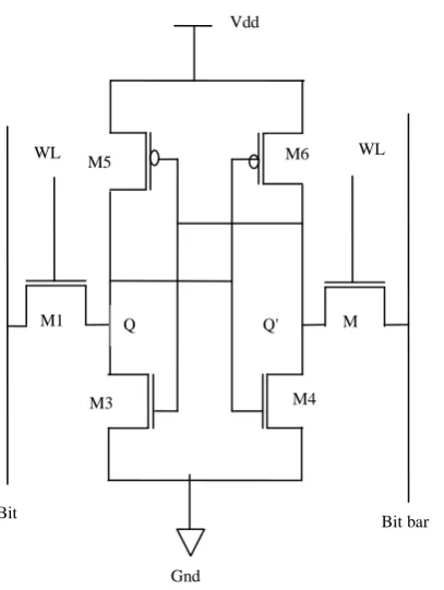
SRAM cell may be designed simply by using cross coupled inverters [5]. The leakage power consumption of the memory cell will be limited to relatively small leakage currents of both CMOS inverters. The only drawback of using the cross coupled inverters, is slightly larger area than resistive load and depletion-load NMOS SRAM Cell. The memory cell consists of a simple CMOS latch in which two inverters connected back to back and two complementary access transistors M1 and M2. The cell will preserve one of its two possible states, as long as the power supply is available. Conventional SRAM cell with 6T is shown in figure 1. There are mainly three states in SRAM cell the write, read and hold states [2]. In the following we describe the states in SRAM cell.
2.1
Hold State
Figure 1: Conventional 6T SRAM cell
2.2 Read State
Read operation starts with pre-charging Bit and Bit bar to high. Within the memory cell M3 and M6 are ON. Asserting the word line, turns ON the M1 and M2 and the values of Q and Q' are transferred to bit-Lines. No current flows through M2, thus M2 and M6 pull Bit bar up to Vdd, i.e., Bit bar = “1” and Bit line discharges through M1 and M3. This voltage difference is sensed and amplified to logic levels by sense amplifiers[5].
2.3 Write State
The value to be written is applied to the bit lines and keep WL= “1”. Thus to write data “0”, we assert Bit=0, Bit bar= “1” and to write data “1”, the Bit = “1”, Bit bar = “0”.
3. LEAKAGE CURRENT COMPONENTS
The leakage current in deep submicron CMOS Technology consists of three major components: junction tunnelling current, sub threshold current and gate leakage current. Since junction tunneling current is a less contribution to the total leakage current in 90nm CMOS technology [3]. In this paper we do not triedto reduce this component of leakage in an SRAM cell. In the following, we describe the gate leakage, sub threshold leakage and junction tunneling leakage currents.
3.1
Sub Threshold Leakage Current
Sub threshold leakage current is the drain- to-source current of a transistor when the gate-to-source voltage is less than the threshold voltage of transistor [3]. The sub threshold current depends exponentially on threshold voltage, which results in large sub threshold current in short channel devices.
3.2 Gate Leakage current
Electrons (holes) tunneling from the bulk silicon through the gate oxide into the gate results in gate leakage current in an NMOS (PMOS) transistor. Gate leakage current consists mainly three components (1) gate to source and gate to drain overlap current (2) gate to channel current, some part of which goes to source and the rest of the part goes to drain (3) gate to
substrate current. In bulk CMOS technology, the gate to substrate leakage current is very less than the overlap leakage current and gate to channel current. On the other hand, the overlap leakage current dominates when the transistor is in off state; gate to channel leakage dictates the gate current in the ON state. Since the gate to source and gate to drain overlap regions are very small than the channel region, the gate leakage current in the OFF state is very small than that of gate leakage current in the ON state [3].
3.3 Junction Tunneling Leakage Current
[image:2.595.312.537.312.692.2]In the reversed biased p-n junction leakage has two main components: one is minority carriers, diffusion near the Edge of the depletion region and the other is due to electron hole pair generation in the depletion region of the reverse biased junction. The junction tunneling current is an exponential function of junction doping and reverse bias voltage across the junction [7]. In 90nm CMOS this is less contribution to the total leakage current so this paper don’t consider to reduce this component in this work. Figure 2 shows the sub threshold leakage current and gate leakage current in SRAM cell storing 0 and when WL=0 [7].
Figure 2: Leakage currents in 6T SRAM cell
M5 M6 WL
Q Q'
M4
Bit bar M3
WL
M 2 M1
Bit
Vdd
Gnd
Subthreshold Leakage current Gate Leakage current M5
M1 0 1
M4
Bit bar M6
M3 WL
M2
Bit
Vdd
Gnd
4. RELATED WORK
4.1 Drowsy Cache
[image:3.595.59.288.285.600.2]In the SRAM cell there are mainly two operations. One is read and other is write operation. It can be assumed as active mode when read and write operation is done. On the other hand when there is no read & write operation, only information preservation is done by the latching phenomena of memory. It is found that there is very low Vdd needed for preservation of data [8]. Drowsy cache method puts memory in a low Vdd when only data preservation is needed. It uses multiple Vdd sources. It supplies high Vdd when actual transmission of data takes place. Leakage currentis reduced as Vdd decreases. Thus, the memory core is put in the low-power drowsy mode when the information preservation is required and in the high-power mode before the access of the contents [9]. The leakage current reduces with the voltage scaling. This reduced leakage current and Vdd results in a much reduction in the leakage power [8]. Figure 3 shows the diagram of drowsy cache.
Figure 3: Drowsy cache 6T SRAM cell
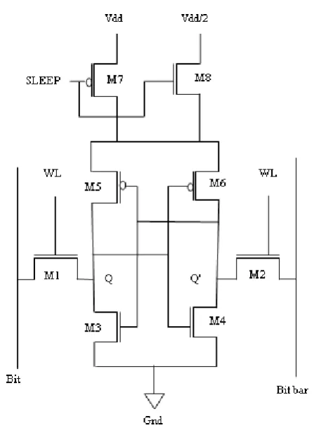
4.2 Hybrid SRAM Cell
To reduce the sub threshold leakage current of a SRAM cell, the Vt of all or some of the transistors of the SRAM cell can be
increased [3]. When the Vt of all transistors in SRAM cell are
increased, the sub threshold leakage current reduction is the highest. However, this has the worst effect on the read delay of the cell. Thus, other configurations which have smaller sub threshold leakage reductions but lower delay penalties. On the other hand, to reduce the gate leakage current of an SRAM cell only the tox of the pull down NMOS transistors and
pass-transistors need to be increased. Since increasing the tox also
increases the Vt of a transistor, in this paper the tox and Vt of a
transistor is not increased at the same time because the delay penalty will be too high [3]. Figure 4 shows the diagram for hybrid SRAM cell. In this work high Vt pull up transistors and
high tox pull down transistors are used for low leakage and high
performance SRAM cell.
Figure 4: Hybrid SRAM cell
5 PROPOSED WORK
The proposed SRAM cell using dual Vdd, high Vt and high tox
together is shown in figure 5. The proposed work shows that when dual Vdd, high Vt, high tox are combindely used, there is
great reduction in the total leakage current. Using high Vt
transistor in SRAM cell sub threshold leakage current of SRAM cell is reduced but delay of read and write operation of SRAM cell is increased. When the Vt of pull up PMOS transistors is
increased, write delay is increased, because in write operation, access transistor and PMOS pull up transistor is involved .When the Vt of access transistors is increased both read and write delay
of SRAM cell is increased, since access transistor are involved in both read and write operation. When the Vt of pull down
NMOS transistors is increased, the read delay of SRAM cell is increased. Since write delay is very less compare to the read delay of SRAM cell so Vt of pull up transistors is increased [3].
To reduce the gate leakage current the SRAM cell tox of
transistors of SRAM cell is increased, since the gate leakage in PMOS transistor is less compared to the NMOS transistor, so in this work the tox of pull down transistors is increased. To reduce
Figure 5: Proposed SRAM cell
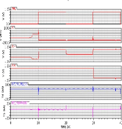
[image:4.595.58.283.80.412.2]6. SIMULATIONS AND RESULTS
[image:4.595.311.526.301.488.2]Figure 6: Simulation result for conventional SRAM cell
Figure 7: Simulation result for drowsy cache SRAM cell
Figure 8: Simulation result for hybrid SRAM cell
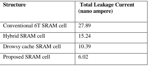
[image:4.595.61.288.488.656.2] [image:4.595.316.525.526.746.2]Table 1: Leakage current in different SRAM cell structures
By the experiment result this is found that total leakage current in conventional SRAM is 27.89 nano ampere, in hybrid SRAM cell 15.24 nano amperes, in drowsy cache it is 10.19 nano ampere, while in proposed work this is 6.02nanoampere.So proposed work is best in terms of leakage power saving in comparison to the other configurations.
7. CONCLUSIONS
In this paper, a structure of the SRAM cell, using high Vt, high
tox and dual Vdd SRAM cell structure is presented. In
comparison to the conventional 6T SRAM cell, the total leakage power is reduced by 45% while the cell is storing data “0” in hybrid SRAM cell, in drowsy cache SRAM cell total leakage saving is 63%, while in proposed SRAM total leakage power saving is 78%.In future this work can be extended to reduce delay penalty and can be applied to larger designs.
8. REFERENCES
[1] Azizi,N., NajmF.N and Moshovos A.,2003 "Low-leakage asymmetric-cell SRAM," , IEEE Transactions on Very Large Scale Integration (VLSI) System, vol. 11, no. 4, pp. 701-715.
[2] ShuklaN. Kr., Singh,R.K., and PattanaikM.,2011 “ Design and Analysis of a Novel Low-Power SRAM Bit-Cell Structure at Deep-Sub-Micron CMOS Technology for
Mobile Multimedia Applications”, International Journal of Advanced Computer Science and Applications, vol. 2, no. 5, pp. 43-49.
[3] Amelifard,B.,FallahF. And Pedram,M., “Reducing the Sub-threshold and Gate-tunneling Leakage of SRAM Cells using Dual-Vt and Dual-Tox Assignment”, www. atrak.usc.edu/~massoud/Papers/dual-vt-tox-sram
tvlsi08.pd, pp 851-860.
[4] Anand, P.R.,Sekhar, P.C.,2011 “Reduce Leakage Currents in Low Power SRAM cell Structures”, IEEE International Symposium on Parallel and Distributed Processing with Applications Workshops, pp 33-38.
[5] Razavipour, G., Afzali, K.A. and Pedram, M.,2009 “Design and Analysis of Two Low-Power SRAM Cell Structures”, IEEE Transactions on Very Large Scale Integration (VLSI) Systems, vol. 17, no. 10, 1551-1555.
[6] Shukla,N. Kr., Singh,,R.K. and Pattanaik,M.,2012 “Analysis of Gate Leakage Current in IP3 SRAM Bit-Cell under Temperature Variations in DSM Technology”, IACSIT International Journal of Engineering and Technology, vol. 4, no. 1,pp. 67-71.
[7] Birla, S.,Shukla,N. Kr., Singh,R.K, and Pattanaik,M.,2010 "Leakage Current Reduction in 6T Single Cell SRAM at 90nm Technology”, in Proceedings of IEEE International Conference on Advances in Computer Engineering, pp. 292-294.
[8] Hulfang Qin, Yu Cao, D. Markovic and A.Vladimirescu, J .Rabaey,2004 "SRAM leakage suppression by minimizing standby supply voltage”, in Proceedings of IEEE International Conference on Quality Electronic Design, pp. 55- 60.
[9] Roy,K., Mukhopadhyay,S., and Mahmoodi H.2003 “Leakage Current Mechanisms and Leakage Reduction Techniques in Deep-Submicrometer CMOS Circuits” proceedings of the IEEE, vol. 91, no. 2, 305-327.
Structure Total Leakage Current
(nano ampere)
Conventional 6T SRAM cell 27.89
Hybrid SRAM cell 15.24
Drowsy cache SRAM cell 10.39