DEVELOPMENT OF AN AC-DC BOOST POWER FACTOR CORRECTION
ZURAIDI BIN MD TAHIR
A project report submitted in partial fulfillment of the requirement for the award of the
Degree of Master of Electrical Engineering
Faculty of Electrical and Electronics Engineering Universiti Tun Hussein Onn Malaysia
ABSTRACT
ABSTRAK
CONTENTS
TITLE i
DECLARATION ii
DEDICATION iii
ACKNOWLEDGEMENT iv
ABSTRACT v
CONTENTS vii
LIST OF TABLE ix
LIST OF FIGURE x
CHAPTER 1 INTRODUCTION 1
1.1 Project Background 1
1.2 Problem Statements 2
1.3 Project Objectives 3
1.4 Project scopes 3
CHAPTER 2 LITERATURE REVIEW 4
2.1 Introduction 4
2.2 Related work 4
2.3 Theories 7
2.3.1 AC to DC Converter 7
2.3.2 Buck 9
2.3.3 Buck Boost 9
2.3.4 Boost 10
2.3.5 Pulse Width Modulation (PWM) 14
2.3.6 Power Factor 16
CHAPTER 3 METHODOLOGY 20
3.1 Project Methodology 20
3.2 Literature Review 22
3.3 Identify Design Requirement 22
3.3.1 Theory of PF 22
3.3.2 Theory of Rectifier 22
3.4 Theory of Boost Converter 24
3.4.1 Circuit operation 24
3.4.2 Pulse-Width Modulation (PWM) 26
3.5 PID controller design 26
CHAPTER 4 RESULTS AND ANALYSIS 28
4.1 Introduction 28
4.2 Simulation result without PFC circuit 29
4.3 With open loop PFC circuit (Boost circuit) 30
4.3.1 Simulation result 31
4.4 With closed loop PFC circuit (Boost circuit) 37
4.4.1 Simulation result 37
CHAPTER 5 CONCLUSION AND RECOMMENDATION 39
5.1 Introduction 39
5.2 Conclusion 39
4.6 Recommendation 40
LIST OF TABLE
4.1 Duty cycle, Power factor and settling time for open 31 loop PFC circuit converter
LIST OF FIGURE
2.1 Converter arrangement for full-bridge rectifier with DC/DC
Converter 5
2.2 (a) Converter arrangement for Bridgeless converter. 5
2.2 (b) Bridgeless Boost PFC 6
2.3 (a) Circuit diagram for Ac to Dc converter or bridge rectifier
convert an alternating current (AC) 7
2.3(b) Ac to Dc converter or bridge rectifier convert an alternating
current (AC) waveform 8
2.4 Current path during operating. 8
2.5 Rectifier circuit with Buck Converter 9
2.6 Rectifier circuit with Buck-Boost Converter 9
2.7 Rectifier circuit with Boost Converter 10
2.8 (a) Configurations of a boost converter, on state of the switch S. 11 2.8 (b) Configurations of a boost converter, off state of the switch S. 11 2.9 Voltages and currents of the boost converter 12
2.10 Gate Voltage on MOSFET 14
2.11 Voltage across the Inductor 14
2.12 Current through the Inductor 15
2.13 Creating a PWM by Comparing Two Waveforms 15 2.14 Creating a PWM by Comparing Two Waveforms 16 2.15 Relation between Active Power, Reactive Power and
Apparent Power. 17
3.2 Simple rectifier without power factor correction (PFC)
draws current from the AC 23
3.3 Model and simulation for circuit without any PFC circuit 24 3.3 Boost converter during switch ON and OFF 25 3.4 Behavior of inductor current [5] (a) Waveforms,
(b) Transistor T gate drive signal x 25
3.5 Model and simulation for a circuit with closed loop PFC
circuit (Boost circuit) 27
4.2 Input voltage, input current and output voltage 29 4.3 Power factor, Active power and Reactive power 29 4.4 PF without power factor corrector (PFC) circuit 30 4.5 Model and simulation for a circuit with PFC circuit
(Boost circuit) 30
4.0 (a) Duty cycle 10% 31
4.0 (b) Duty cycle 20% 32
4.0 (c) Duty cycle 30% 32
4.0 (d) Duty cycle 40% 33
4.0 (e) Duty cycle 50% 33
4.0 (f) Duty cycle 60% 34
4.0 (g) Duty cycle 70% 34
4.0 (h) Duty cycle 80% 35
4.0 (i) Duty cycle 90% 35
4.6 Input voltage, input current and output voltage 36 4.8 PF with open loop PFC circuit (Boost circuit) 36 4.9 Model and simulation for a circuit with closed loop PFC
circuit (Boost circuit) 37
CHAPTER 1
INTRODUCTION
1.1 Project Background
Power factor is defined as the cosine of the angle between voltage and current in an ac circuit. There is generally a phase difference Ø between voltage and current in an ac circuit. cos Ø is called the power factor of the circuit. If the circuit is inductive, the current lags behind the voltage and power factor is referred to as lagging. However, in a capacitive circuit, current leads the voltage and the power factor is said to be leading.
In a circuit, for an input voltage V and a line current I, VIcos Ø – the active or real power in watts or kW. VIsin Ø - the reactive power in VAR or kVAR. VI- the apparent power in VA or kVA.
𝑃𝑜𝑤𝑒𝑟 𝑓𝑎𝑐𝑡𝑜𝑟 = 𝑅𝑒𝑎𝑙 𝑃𝑜𝑤𝑒𝑟 (𝐴𝑣𝑒𝑟𝑎𝑔𝑒) 𝐴𝑝𝑝𝑎𝑟𝑒𝑛𝑡 𝑝𝑜𝑤𝑒𝑟
Where, the apparent power is defined as the product of rms value of voltage and current.
In a purely resistive AC circuit, voltage and current waveforms are in step (or in phase), changing polarity at the same instant in each cycle. Where reactive loads are present, such as with capacitors or inductors, energy storage in the loads result in a time difference between the current and voltage waveforms. This stored energy returns to the source and is not available to do work at the load. A circuit with a low power factor will have thus higher currents to transfer at a given quantity of power than a circuit with a high power factor.
In recent years, there have been increasing demands for high power factor and total harmonic distortion in the current drawn from the utility. With the stringent requirements of power quality [1], power factor corrector has been an active research topic in power electronics, and significant efforts have been made on the developments of the power factor corrector converters [2]. In general, the continuous-conduction mode (CCM) boost topology has been widely used as a power factor corrector converter because of its simplicity and high power capability. It can be used with the universal input voltage range.
The work initially involves simulation of basic power electronic circuits and the analysis of the current and voltage waveforms. All the simulation work is done in MATLAB Simulink environment and the results are attached herewith. After the performance of the proposed converter is acceptable, the proposed rectifier prototype is built to verify the operation; the critical relationships of voltage boost and simulation results are presented.
1.2 Problem Statements
improved power factor and reduced harmonics content in input line currents as well as voltage regulation during power line over-voltage and under voltage conditions.
1.3 Project Objectives
This project has been developed to enhance the achievement in the following matter:- a) Develop modelling of Ac to Dc converter.
b) Develop simulation modeling of open loop PFC of Boost Converter using software MATLAB simulink.
c) Develop simulation modeling of closed loop PFC of Boost Converter using software MATLAB simulink.
1.4 Project scopes
CHAPTER 2
LITERATURE REVIEW
2.1 Introduction
Conventionally, ac-dc converters, which also called rectifier, are developed using diodes and thyristors to provide controlled and uncontrolled dc power with power flow. These converters can be subclasified into 4 types as boost, buck, buck-boost and multilevel with unidirectional and bidirectional power flow [4]. There are three basic types of ac to dc converter circuits with PFC is discuss in this chapter, termed as buck, boost and buck boost with unidirectional power flow and also discuss about power factor.
2.2 Related work
M. Gopinath and D. Yogeetha (2009) performed a comparative evaluation of the Bridgeless topology followed by the full-bridge with 1 DC/DC converter. Several issues will be highlighted and most of them are concerned on the efficiency of the converter at low power operation which is 300W or less. For Full-bridge with 1 DC/DC converter, only one DC/DC converter is used, and that’s the reason why this topology is classified as single-stage PFC. Figure 2.1: shows the general circuit diagram for single-stage PFC circuit.
Figure 2.1: Converter arrangement for full-bridge rectifier with 1DC/DC converter
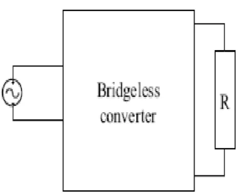
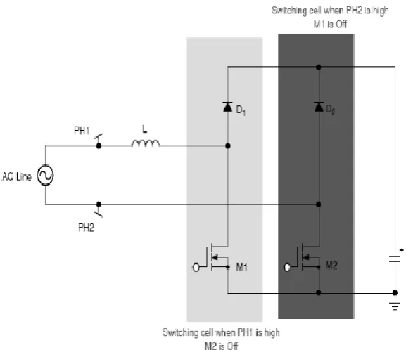
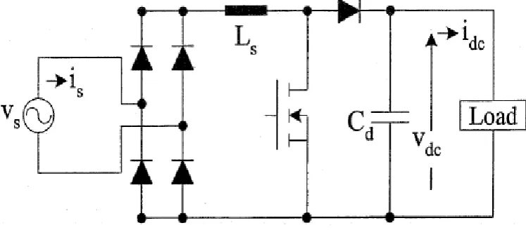
For Bridgeless converter as shown in Figure 2.2 (a): topology does not have rectifier circuit operated throughout the full cycle and that’s the reason for its name. Figure 2.2(b) shows one of the earliest topology in this class which is called the Bridgeless Boost PFC
[image:13.595.190.423.488.677.2]Figure 2.2 (b): Bridgeless Boost PFC.
Based on the Two PFC topologies, it is found that the best efficiency is obtained from the Bridgeless topology followed by the full-bridge with 1 DC/DC converter. It is found that by using less number of components, the efficiency can be improved up to 8% and in some cases up to 10% as explained previously. However, the Bridgeless converters discussed in this paper were unable to be used as switch mode power supplies due to its output voltage which is not regulated at 19V. On top of that, it can be observed that several works have been using variable switching frequency especially for fully DCM or CCM/DCM boundary operation [6].
A. Jangwanitlert and J. Songboonkaew applied and testing a soft-switch ac-dc symmetrical boost converter with power factor correction. The rectifier is modified boost voltage that is well suited for low line input applications and operated with half of the switch voltage stress than those found in standard boost converter. Soft- witching in the boost converter is achieved under Zero-Voltage Switching (ZVS) turn on and Zero-Current Switching (ZCS) at turn on, quasi resonant technique [7].
[image:14.595.175.464.80.329.2]eventually interested in using boost topologies for PFC applications. The exposition of six types of arrangement is expected to present the evolution of the boost converter and also provide easy selection of an appropriate topology for a given application. While dedicated to highlight some of the main characteristics regarding the converters, the paper seeks to motivate the reader to analyze some of the most important publications related to the theme by adequately citing them.
2.3 Theories
2.3.1 AC to DC Converter
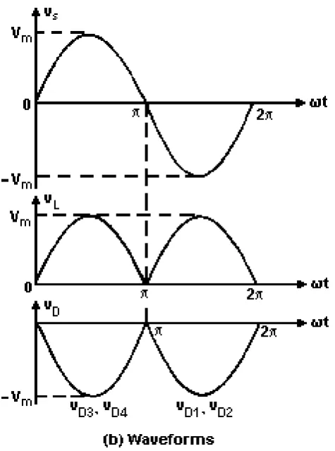
Ac to Dc converter or bridge rectifier convert an alternating current (AC) input into direct current a (DC) output, refer Figure 2.3. Figure 2.4 below show the current path during operating. When ac voltage is applied to the four-diode full-wave bridge rectifier, the positive half of the sine wave will be rectified by diodes 1 and 3. The negative half of the sine wave is rectified by diodes 2 and 4. From the top circuit in Fig. 2.4 notice that the positive half-cycle of the ac is shaded, and the first half-wave is shaded to indicate the output for this part of the circuit. The bottom circuit shows the negative half of the sine wave being rectified. The path the electrons would travel through the bridge is also shown. Notice that electron flow is always against the arrows of the diodes.
[image:15.595.162.460.513.651.2]Figure 2.3(b): Ac to Dc converter or bridge rectifier convert an alternating current (AC) waveform
[image:16.595.108.525.487.707.2]2.3.2 Buck
[image:17.595.126.526.252.380.2]A buck converter is shown in Figure 2.5 below. In principle, it is a combination of diode rectifier with step down chopper with input and output filter. Its performance is improved using a ripple filter at dc output for reducing harmonics in ac mains and ripples at dc output voltage. Nowadays, it is also developed using a diode rectifier with filter and various combinations of dc–dc converter with and without high-frequency transformer isolation [4].
Figure 2.5: Rectifier circuit with Buck Converter
2.3.3 Buck Boost
A buck boost converter is shown in Figure 2.6 below. In principle, it is a combination of diode rectifier with buck–boost dc–dc converters [4].
[image:17.595.132.525.518.647.2]2.3.4 Boost
[image:18.595.134.508.210.374.2]A boost converter is shown in Figure 2.7 below. In principle, it is a combination of diode bridge rectifier and step up dc chopper with filtering and energy storage elements. These converters are extensively used in electronic ballast, power supplies, variable-speed ac motor drives in compressor, refrigerator, pumps, fans, etc [4].
Figure 2.7: Rectifier circuit with Boost Converter
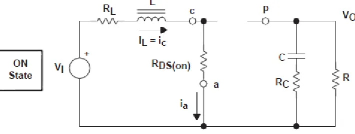
The key principle that drives the boost converter is the tendency of an inductor to resist changes in current. In a boost converter, the output voltage is always higher than the input voltage. When the switch is closed, current flows through the inductor in clockwise direction and the inductor stores the energy. Polarity of the left side of the inductor is positive. When the switch is opened, current will be reduced as the impedance is higher. Therefore, change or reduction in current will be opposed by the inductor. Thus the polarity will be reversed (means left side of inductor will be negative now). As a result two sources will be in series causing a higher voltage to charge the capacitor through the diode D.
The switch must of course be opened again fast enough to prevent the capacitor from discharging too much.
Figure 2.8 (a): Configurations of a boost converter, on state of the switch S.
Figure 2.8 (b): Configurations of a boost converter, off state of the switch S.
[image:19.595.138.494.121.256.2] [image:19.595.136.496.344.476.2]Figure 2.9: Voltages and currents of the boost converter
From the figure 2.9, the relationship of voltage and current for an inductor is:
, or (2.1)
(2.2) For a constant rectangular pulse:
(2.3) From this we can see that the current is a linear ramp, when the voltage is a constant pulse. When the transistor switches on the current is:
, or (2.4)
and when the transistor switches off the current is:
, or (2.6)
(2.7) Where VD is the voltage drop across the diode, and VTrans is the voltage drop across
the transistor. Note that the continuous/discontinuous boundary occurs when io is
zero. By equating through delta i, we can solve for 𝑉𝑜𝑢𝑡:
(2.8)
(2.9) We can also solve for the duty cycle as follows,
(2.10)
(2.11) If we neglect the voltage drops across the transistor and diode then:
𝑉
𝑜𝑢𝑡=
𝑉𝑖𝑛1−𝐷
(2.12)
2.3.5 Pulse Width Modulation (PWM)
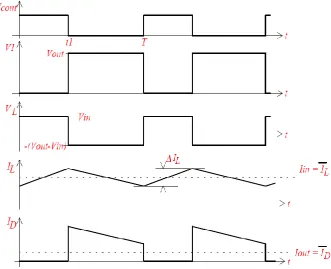
[image:22.595.189.443.257.406.2]The fundamental principle involved in making a boost converter is creating a square pulse to control the switching of the MOSFET. This square pulse is called the duty cycle and this duty cycle (D) controls the output voltage. The transfer function is derived by the following set of equations. Figure 2.10 is the ideal gate voltage to be able to switch the MOSFET and create a boosted output voltage. The y-axis shows VGS (V) and the x-axis shows the time interval of the signal.
Figure 2.10: Gate Voltage on MOSFET
As the MOSFET gate switches to 0V, current is no longer sourced directly to ground, thus forcing current to the output. Conversely, when the gate is switched to 5V, the current in the inductor flows directly from the drain to the source which is connected to ground creating different voltages across the inductor. The voltage across the inductor is shown in Figure 2.11 and the voltage changes with the duty cycle.
[image:22.595.191.445.565.705.2]The voltage across the inductor while VGS is at 5V is equal to VIN. The voltage across the inductor while VGS is at 0V is equal to VIN-VOUT. Because the constant voltages are applied to the inductor, the current through the inductor ramps up and down linearly with time. Based on the slope of the rising and falling slopes of the current through the inductor and the fact that the time duration is a known entity, the transfer function can be computed. The relationship between the slope and time duration is shown in Figure 2.12 where the y-axis represents an arbitrary current value and the x-axis represents the time interval.
Figure 2.12: Current through the Inductor
The duty cycle of VGS is what allows a boost converter to function. As D
increases, the gain also increases. In order to create a duty cycle, a PWM needed to be created. There are several methods of creating a PWM. The first of which is to use a function generator that can output an adjustable duty cycle square wave at a frequency up to 20MHz. However, most function generators cannot produce square waves up to 20MHz. The next method for creating a PWM is to compare a ramp wave to a DC value. As the DC value decreases or increases, the duty cycle increases or decreases respectively.
[image:23.595.184.450.606.724.2]A triangle waveform is one wave that can be used to create a PWM. The other waveform is a saw tooth wave.
Figure 2.14: Creating a PWM by Comparing Two Waveforms
Either a saw tooth or a triangle wave would work to create a PWM needed for the boost converter, but the triangle is an easier shape to create and the Triangle has a few distinct advantages over the saw tooth. “An intrinsic advantage of modulation using a triangle carrier wave is that the odd harmonic sideband components around odd multiples of the carrier fundamental and even harmonic sideband components around even multiples of the carrier fundamental are eliminated.” [9] Additionally, a small change in the input voltage using the triangle wave will result in a larger change in the PWM than when using a saw tooth.
2.3.6 Power Factor
PF is expressed as decimal number between zero and one (0 and 1). A non-corrected
power supply with a typical PF equal to 0.65 will draw approximately 1.5 times
greater input current than a PFC supply (PF = 0.99) for the same output loading. The
non-corrected supply requires additional AC current to be generated which is not
consumed by the load, creating I2R losses in the power distribution network. Power
factor also defined as a ratio between real powers flowing to the load to the apparent power in the circuit, Figure 2.6.
𝑃𝑜𝑤𝑒𝑟 𝑓𝑎𝑐𝑡𝑜𝑟 = 𝑅𝑒𝑎𝑙 𝑃𝑜𝑤𝑒𝑟 (𝐴𝑣𝑒𝑟𝑎𝑔𝑒) 𝐴𝑝𝑝𝑎𝑟𝑒𝑛𝑡 𝑝𝑜𝑤𝑒𝑟
distorts the wave shape of the current drawn from the source, the apparent power will be greater than the real power.
Figure 2.15: Relation between Active Power, Reactive Power and Apparent Power.
In a linear system, the load draws purely sinusoidal current and voltage, the current and voltage, hence the power factor is determined only by the phase difference between voltage and current, where
Power Factor (PF) = cos 𝜃
In power electronic system, due to the non-linear behavior (Figure 2.16) of the active switching power devices, the phase angle representation alone is not valid. A non linear load draws typical distorted line current from the line. The PF of distorted waveforms is calculated as below:
The fourier representation for line current isand line voltage vsare given by,
𝑖𝑠 = 𝐼𝐷𝐶 + 𝐼𝑠𝑛 sin 𝑛𝜔𝑡 + 𝜃 (2.13)
𝑣𝑠 = 𝑉𝐷𝐶 + 𝑉𝑠𝑛sin 𝑛𝜔𝑡 + 𝜃 (2.14)
The line current is non-sinusoidal when the load is nonlinear. For sinusoidal voltage and non- sinusoidal current the PF can be expressed as
𝑃𝐹 =𝑉𝑟𝑚𝑠𝑉 𝐼1𝑟𝑚𝑠
𝑃𝐹 =𝐼1𝑟𝑚𝑠
𝐼𝑟𝑚𝑠 cos 𝜃 (2.16)
𝑃𝐹 = 𝐾𝑝cos 𝜃 where, 𝐾𝑝 = 𝐼𝐼𝑟𝑚𝑠1𝑟𝑚𝑠 , 𝐾𝑝 ∈ 0,1 (2.17)
[image:26.595.142.501.206.304.2]cos 𝜃 is the displacement factor of the voltage and current and 𝐾𝑝is the purity factor or the distortion factor.
Figure 2.16: Input current waveform for single phase bridge rectifier
2.3.7 Introduction to PID controller
A proportional-integral-derivative controller (PID controller) is a generic control loop feedback mechanism (controller) widely used in industrial control systems. A PID controller calculates an "error" value as the difference between a measured process variable and a desired set point. The controller attempts to minimize the error by adjusting the process control inputs, figure 2.17.
The PID controller calculation (algorithm) involves three separate constant parameters, and is accordingly sometimes called three-term control: the proportional, the integral and derivative values, denoted P, I, and D. Heuristically, these values can be interpreted in terms of time: P depends on the present error, I on the accumulation of past errors, and D is a prediction of future errors, based on current rate of change.
A PID controller has proportional, integral and derivative terms that can be represented in transfer function form as
𝐾 𝑠 = 𝐾𝑝 +𝐾𝑖
𝑠 + 𝐾𝑑𝑠 (2.18)
the controller can provide control action designed for specific process requirements [10]. The proportional term drives a change to the output that is proportional to the current error. This proportional term is concerned with the current state of the process variable.
The integral term (𝐾𝑖) is proportional to both the magnitude of the error and
the duration of the error. It (when added to the proportional term) accelerates the movement of the process towards the set point and often eliminates the residual steady-state error that may occur with a proportional only controller.
The rate of change of the process error is calculated by determining the differential slope of the error over time (i.e., its first derivative with respect to time). This rate of change in the error is multiplied by the derivative gain (𝐾𝑑) [10].
[image:27.595.112.526.446.603.2]In the absence of knowledge of the underlying process, a PID controller has historically been considered to be the best controller. By tuning the three parameters in the PID controller algorithm, the controller can provide control action designed for specific process requirements. The response of the controller can be described in terms of the responsiveness of the controller to an error, the degree to which the controller overshoots the setpoint and the degree of system oscillation.
Figure 2.17: PID control logic
CHAPTER 3
METHODOLOGY
3.1 Project Methodology
Figure 3.1 Flowchart of project methodology
Design Ac-Dc Converter with closed loop PFC circuit (Boost circuit)
- The PID value is set using trial and error - Test run the design
Confirm on the result obtained
Conclusion based on the results obtained
END
No
SUCCESS
Design Ac-Dc Converter with open loop PFC circuit (Boost circuit)
- Determine the component parameter
- Test run the design with several value of the duty cycle
SUCCESS
START
Define problem statement
- Define objectives and the scopes of the project
- Literature review writing
.- Finalise concepts and methodology
Design Ac-Dc Converter
- Determine the component parameter - Test run the design
No
No
Yes
Yes
3.2 Literature Review.
Generally, the purpose of a review is to analyze critically a segment of a published body of knowledge through summary, classification, and comparison of prior research studies, reviews of literature, and theoretical articles. The entire of the literature review of this project was included at chapter 2.
3.3 Identify Design Requirement
3.3.1 Theory of PF
Power factor is characteristic of alternating current (AC) and the values of PF are between 0.0 to 1.0. The higher value of PF is the better PF. A non-corrected power supply with a typical PF equal to 0.65 will draw approximately 1.5 times greater input
current than a PFC supply (PF = 0.99) for the same output loading. For this project, studies are made to Ac to Dc converter without PFC and Ac to Dc converter with PFC, PF between these converters are record and compare.
3.3.2 Theory of Rectifier
Figure 3.2: Simple rectifier without power factor correction (PFC) draws current from the AC
From the information, Ac-Dc full wave converter is tested using MATLAB/Simulink. The design is shown in figure 3.3.
Figure 3.3 Model and simulation for circuit without any PFC circuit Rectifier
AC Source
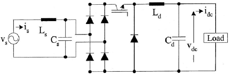
[image:31.595.112.562.431.715.2]3.4 Theory of Boost Converter
Many circuits and control methods using switched-mode topologies have been developed to comply with standard. The active PFC’s employ six basic converter topologies
1) Buck Corrector 2) Boost Corrector 3) Buck-Boost corrector
4) Cuk, Sepic and Zeta Correctors
We go for boost rectifiers which is one of the most important high power factor
rectifiers from a theoretical and conceptual point of view. It is obtained from a
classical non-controlled bridge rectifier, with the addition of transistor, diode and
inductor.[5]
3.4.1 C ircuit operation
The input current is(t) is controlled by changing the conduction state of transistor. By
switching the transistor with appropriate firing pulse sequence, the waveform of the input current can be controlled to follow a sinusoidal reference, as can be observed in the positive half wave in Figure3.4 (a,b). This figure shows the reference inductor current iLref, the inductor current iL, and the gate drive signal x for transistor.
REFERENCES
1. J. C. Salmon, “Circuit topologies for single-phase voltage-doubler boost rectifiers,” in Proc.IEEE Applied Power Electronics Conf., Mar. 1992, pp. 549–556.
2. D. Tollik and A. Pietkiewicz, “Comparative analysis of 1-phase active power factor correction topologies,” in Proc. Int. Telecommunication Energy Conf., Oct. 1992, pp. 517–523.
3. T. Ernö and M. Frisch, “Second generation of PFC solutions,” Power Electronics Europe, Issue, pp. 33-35, 2004.
4. Bhim Singh, Brig N. Singh, Ambrish Chandra, Kamal Al-Haddad, Ashish Pandey and Dwarka P. Kothari,”A Review of Single-Phase Improved Power Quality Ac-DC Converters” in IEEE Transactions on Industrial Electronic, Vol 50, No. 5, October 2003, pp. 962-981.
5. Rashid M., Power Electronics Handbook.
6. M. Gopinath and D. Yogeetha, “Efficiency Analysis of Bridgeless PFC Boost Converter with the Conventional Method” International Journal of Elektronic Engineering Research, ISSN 0975 – 6450 Volume 1 Number 3 (2009) pp. 213 – 221.
7. Jangwanitlert, A.; Songboonkaew, J.; , "A Soft-Switched AC-DC Symmetrical Boost Converter with Power Factor Correction," Power Electronics and Drive Systems, 2007. PEDS '07. 7th International Conference on , vol., no., pp.784-788, 27-30 Nov. 2007
9. Rus, D. C., N. S. Preda, I. I. Incze, Maria Imecs, and Cs Szab. "Comparative Analysis of PWM Techniques:." IEEExplore (2010). Print.
10. Dorf, Richard C. and Robert H. Bishop, Modern Control Systems, 9th ed., Prentice–Hall Inc., New Jersey-07458, USA, 2001, Chapters 1, 5, pp. 1-23, pp. 173-206.