doi:10.4236/msa.2010.14033 Published Online October 2010 (http://www.SciRP.org/journal/msa)
Effect of Mn Doping on Solvothermal Synthesis of
CdS Nanowires
Zinki Jindal1,2, Narendra Kumar Verma1
1School of Physics & Materials Science, Thapar University, Patiala, India; 2Department of Physics, Sir Padampat Singhania University,
Udaipur, India.
Email: [email protected]
Received May 20th, 2010; revised July 26th, 2010; accepted September 27th, 2010.
ABSTRACT
High aspect ratio (up to 100) CdS nanowires having average diameter of 15 nm and length varying from 0.5-1.5 μm have been synthesized using solvothermal technique in ethylenediamine as a solvent at 120℃ and the effect of Mn dop- ing on morphology and optical properties has been studied. X-ray diffraction analysis shows the typical inter-planar spacing and the diffraction peaks corresponding to the hexagonal wurzite phase of CdS. Morphological study has been done through scanning electron microscopy (SEM) and transmission electron microscopy (TEM) and the optical studies have been conducted through absorption spectra and room temperature photoluminescence (PL).
Keywords: Nanomaterials, Semiconducting Cadmium Compounds, Growth from Solutions, Nanostructures, Nucleation
1. Introduction
One dimensional (1D) nanostructures are considered to be critical building blocks for nanoscale electronic and optoelectronic devices and have received tremendous attention since the discovery of carbon nanotubes [1-9]. CdS is one of the most studied materials due to its exten- sive applications in photoelectric conversion in solar cells and light-emitting diodes in flat panel displays [10]. CdS nanowires have been synthesized by several tech- niques. For instance, the growth of thin CdS nanowires (−20 nm thick) has been achieved by a laser ablation technique or chemical vapor deposition (CVD) process based on a gold nanocluster catalyzed vapor-liquid-solid (VLS) growth mechanism [11]. CdS nanowires with di- ameters of 30-70 nm have also been synthesized simply by thermal evaporation of CdS powders [12]. Neverthe- less, the above mentioned methods need some special instruments, harsh conditions, and/or relatively high per- formance temperature (over 800℃). Uniform nanowires of CdS could also be obtained in the channels of various templates, such as anodic aluminum oxide (AAO) mem- brane [13], polymer gels [14], micelles [15], and so on [16]. Although the template-directed methods are effect- tive in preparing nanowires with uniform and controlla- ble dimensions, they usually lead to a complicated proc- ess and also impurities due to the incomplete removal of
the templates, and the yields are relatively low. Moreover, high aspect ratio (length to diameter) CdS nanowires have also been prepared by solvothermal process [9, 17-19], which may provide a more promising technique for preparing CdS nanowires than conventional methods in terms of cost and potential for large-scale production. The modification in the properties of the semiconducting nanomaterials can be done by tailoring their energy band structure [20,21] with ion implantation, ion doping, chemical vapor ion doping [22]. Nanomaterials doped with optically active luminescence centers create new opportunities for luminescence research and also for the application of nanometer-scale structured materials. Many research groups have studied the optical, magnetic and fluorescent properties of Mn-doped CdS nanocrys- tals [23-26]. But most studies focus on doped CdS nanoparticles. However, there is a need of studying the changes in the properties of the 1D nanoforms (undoped as well as doped) for their potential application in nano- scale optoelectronic devices.
luminescence properties.
2. Experimental
The synthesis of CdS nanowires has been carried out in a closed cylindrical teflon-lined stainless steel chamber. All of the chemical reagents used in this experiment were of analytical grade and used without further purification. Cadmium foils were used as a substrate and also as an additional source of cadmium. 0.005 M cadmium nitrate [Cd(NO3)2.4H2O] along with 0.015 M thiourea [CSN2H4]
were taken with 70ml of ethylenediamine (En) which acted as the solvent in the teflon chamber (capacity ~100 ml). Mn doped CdS nanostructures were also prepared by adding 5 mmol and 10 mmol manganese acetate (Mn (CH3COO)2). The properly sealed teflon-lined stainless
chamber was maintained at temperature of 120℃ for 24 hours in an electric oven and afterwards, it was allowed to normally cool down to room temperature. The foil and the yellow colored precipitates were collected from the reaction vessel and were washed with de-ionized water and ethanol several times and subsequently dried in air at 50℃ for 6-12 hours.
The products were characterized by Panalytical’s X’Perto Pro X-ray diffraction machine using the copper characteristic wavelength of 1.5418 Å. Microstructures of the nanoforms were studied through scanning electron microscopy (SEM, FEI, Nova 200 NanoLab) and trans- mission electron microscopy (TEM, Hitachi, H-7500). Optical absorption spectra of the products, dispersed in spectroscopic grade ethanol, were recorded by a Hitachi 330 UV-Vis spectrophotometer. Photoluminescence (PL) measurements were carried out at room temperature with a luminescence spectrometer (Varian Cary Eclipse fluo- rescence spectrophotometer) using 336 nm as the excita- tion wavelength.
[image:2.595.314.533.90.240.2]3. Results and Discussion
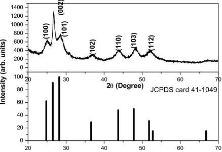
Figure 1 shows the XRD pattern of the synthesized CdS nanowires with all the diffraction peaks corresponding to the hexagonal wurzite phase of CdS. These match well with those in the JCPDS Card (Joint Committee on Powder Diffraction Standards, Card no. 41-1049), as shown in
Figure 1. No impurity peaks were detected, indicating high purity product. In addition, the intense and sharp diffraction peaks suggest that the obtained product is well crystallized. The d-spacing of the CdS nanowires have been calculated using the XRD analysis and com- pared with the standard JCPDS data (Table 1). The cor- responding (hkl) values are illustrated in the table.
In case of solvothermal synthesis, temperature and concentration plays an important role in the formation of crystal structure, shape and size of the nanoforms. The
20 30 40 50 60 70
0 200 400 600 800 1000 1200 1400 (10 0) (0 02 ) (1 01 ) (10 2) (11 0) (10 3) (1 12 ) Inten sity (arb . un it s) 2 (Degree)
20 30 40 50 60 70
0 20 40 60 80 100
JCPDS card 41-1049
[image:2.595.307.538.331.468.2]Figure 1. XRD pattern of the CdS nanowires revealing their hexagonal wurzite phase, and the standard JCPDS card No. 41-1049.
Table 1. The comparison of d-values, obtained from XRD and JCPDS, and illustration of the corresponding (hkl) val- ues.
Peak 2θo d
XRD(Å) dJCPDS(Å) (hkl)
1. 25.04 3.5561 3.5861 100
2. 26.78 3.3289 3.3599 002
3. 28.52 3.1296 3.1630 101
4. 37.07 2.4251 2.4519 102
5. 43.88 2.0632 2.0705 110
6. 48.08 1.8924 1.8998 103
7. 52.09 1.7557 1.7627 112
mechanism behind the formation of nanorods, in pres- ence of ethylenediamine (En) as chelating agent, has al- ready been discussed by many researchers [18]. En reacts with the Cd2+ ions to form Cd-En complex lamellar
products, which react with the S2- ions to produce CdS-En
lamellar materials. The high temperature leads to the breakage of volatile amine groups giving rise to lamel- lar-to-rod transitions. This is known to proceed via the rolling mechanism [27].
The morphology and the dimensions of the nanowires were studied through scanning electron microscopy (SEM) and transmission electron microscopy (TEM).
(a) (b)
[image:3.595.69.526.83.541.2](c) (d)
Figure 2. SEM images of (a, b) undoped and (c) 5 mmol (d) 10 mmol Mn doped CdS nanostructures.
ing with Mn, and on increasing the concentration of Mn from 5 to 10 mmol (as per the experiment performed), it has been observed that this lamellar-to-rod transition has decreased. Figure 2(c) shows the fragmentation of these Mn doped CdS-En (5 mmol Mn) lamellae to higher level as compared with those of Figure2(d) (10 mmol Mn), where this fragmentation is still in the initial stage. The reason behind this inhibition of CdS nanowire growth on addition of Mn dopant is not clear at this moment. The Mn dopant is considered to bind to the most stable sur- face sites formed during the nanowire nucleation, which inhibits the advancement of the growth in the particular direction [28].
Figures 3(a, b, c, d) show the formation of high aspect ratio (up to 100) CdS nanowires. The diameter of the synthesized nanowires ranges from 9 to 18 nm, whereas the length varies from 0.5 to 1.5 μm. Figures 3(a, b)
shows the bundles of the CdS nanowires where the indi- vidual nanowires can be well distinguished, whereas
Figures 3(c, d) shows the individual nanowires. More- over, the flexibility of the CdS nanowires can be ob- served from Figures 3(c, d), by their wavy nature.
(a) (b)
(c) (d)
Figure 3. (a-d) TEM images of undoped CdS nanowires.
spectively, as compared with that of CdS bulk materials (515 nm). The band gap energies were calculated from the differential minima, which varied from 2.48 eV to 2.44 eV on doping with Mn. The observed diameters of the CdS nanowires are well above its Bohr`s exciton ra- dius (−2.8 nm), therefore, this shift in the band gap ener- gies may not be related with quantum confinement effect. The small change in the band gap values may be attrib- uted to the direct energy transfer between the semicon- ductor excited states and the 3d levels of the Mn2+ ions,
[image:4.595.73.527.85.572.2]400 500 600 700 400 450 500 550 600 650 700
CdS pure 469 nm 460 nm A b sorbanc e ( ar b . uni ts )
Wavelength (nm)
[image:5.595.62.282.83.258.2]CdS:Mn
Figure 4. Optical absorbance of the as synthesized CdS, undoped and doped with Mn (5 mmol), nanowires.
460 480 500500500 520 540 560 580 600600600 620 640
(i) (iii) (ii) 481 nm 599 nm 595 nm 555 nm 517 nm Inten sity (ar b . u n its) Wavelength (nm)
Figure 5. Room temperature PL spectra of (i) undoped CdS and (ii) 5 mmol (iii) 10 mmol Mn doped CdS nanowires (λex ~ 336 nm).
while the trapped emission is broad and stokes-shifted. CdS is a wide-band-gap (Eg = 2.42 eV) semiconductor
and has typically two emission bands: green band (exci- tonic emission) around 518 nm and the red band (as- cribed to trap of surface states) at about 732 nm [31]. But due to their 1D geometrical characteristic at the nanome- ter scale, CdS nanowires are expected to have different physical properties from their bulk counterparts [32]. Moreover, it is also believed that nanowires with high aspect ratio have more surface and subsurface defects such as grain boundaries and sulfur/cadmium related defects. These would definitely exert an influence on the PL properties of the CdS nanowires. Room temperature PL spectra of undoped CdS nanowires exhibit a weak and sharp emission at −481 nm and a broad green emis- sion band centered at −517 nm. The weak emission band
at shorter wavelengths is attributed to the direct transition from the conduction to the valence band [33]. This indi- cates that the particle crystallinity is rather high. The main luminescence band is broad and is attributed to CdS trap emission. The electrons and holes, after excitation across the band edge, trickle down non-radiatively to the surface states lying in the bandgap region. Radiative de-excitation across the surface states in CdS nanowires gives rise to green fluorescence observed at around 517 nm. On addition of Mn (5 mmol) dopant, the intensity of the direct transition has been found to decrease and the broad band, red shifted to 595 nm, which is similar to the Mn emission in bulk CdS:Mn due to an internal Mn2+
transition (4T
1 – 6A1). On increase in the concentration of
Mn (5 to 10 mmol), this broad band has red shifted to ~ 599 nm, indicating that the Mn2+ concentration is suffi-
cient to influence the crystal-field splitting between 4T 1
and 6A
1 states [34]. Moreover, a broad band, centered
around 555 nm, has evolved on the increase of Mn con- centration, which may be attributed to the deep surface trap recombination, unlike from defect related states [35].
4. Conclusions
In summary, we have studied the effect of Mn doping on the solvothermal synthesis of CdS nanowires. The mor- phological study showed that the lamellar-to-rod transi- tion of CdS has decreased on increase in concentration of Mn dopant, while keeping all the other reaction condi- tions same, like: temperature, time duration, solvent, concentration of Cd and S precursors. This might be due to the binding of Mn to the most stable sites during the nanowires nucleation, leading to the inhibition of the growth in a particular direction. CdS nanowires exhibit broad green emission and on addition of Mn, 5 mmol, this band has red shifted to characteristic 595 nm. On further increase of Mn concentration to 10 mmol, there is additional red shift of 4 nm of this broad band. And an- other emission centered around 555 nm has been ob- served, possibly due to deep surface trap recombination. In future, due to the potential applications of CdS: Mn nanowires in the field of optoelectronics, there is need of more detailed study regarding the mechanism.
5. Acknowledgements
We acknowledge Defence Research & Development Organisation (DRDO), Government of India, for their generous funding for the research work vide their letter No. ERIP/ER/0504321/M/01/855 dated 16th December 2005.
REFERENCES
[image:5.595.63.281.299.476.2]Nature, Vol. 354, No. 6348, 1991, pp. 56-58.
[2] Z. L. Wang and J. H. Song, “Piezoelectric Nanogenera-tors Based on Zinc Oxide Nanowire Arrays,” Science, Vol. 312, No. 5771, 2006, pp. 242-246.
[3] Y. N. Xia, P. D. Yang, Y. G. Sun, Y. Y. Wu, B. Mayers, B. Gates, Y. D. Yin, F. Kim and Y. Q. Yan, “One-Dimen- sional Nanostructures: Synthesis, Characterization, and Applications,” Advanced Materials, Vol. 15, No. 5, 2003, pp. 353-389.
[4] W. Q. Han, S. S. Fan, Q. Q. Li and Y. D. Hu, “Synthesis of Gallium Nitride Nanorods through a Carbon Nano-tube-Confined Reaction,” Science, Vol. 277, No. 5330, 1997, pp. 1287-1289.
[5] A. M. Morales and C. M. Lieber, “A Laser Ablation Method for Synthesis of Crystalline Semiconductor Nanowires,” Science, Vol. 279, No. 5348, 1998, pp. 208- 211.
[6] J. R. Heath, P. J. Kuekes, G. S. Snider and R. S. Williams, “A Defect-Tolerant Computer Architecture: Opportunities for Nanotechnology,”Science, Vol. 280, No. 5370, 1998, pp. 1716-1721.
[7] J. T. Hu, O. Y. Min, P. D. Yang and C. M. Lieber, “Con-trolled Growth and Electrical Properties of Heterojunc-tions of Carbon Nanotubes and Silicon Nanowires,” Na-ture, Vol. 399, No. 6731, 1999, pp. 48-51.
[8] C. N. R. Rao, F. L. Deepak, G. Gundiah and A. Govinda-raj, “Inoranic Nanowires,” Progress in Solid State Chem-istry, Vol. 31, No. 1-2, 2003, pp. 5-147.
[9] S. Kar, S. Santra and H. Heinrich, “Fabrication of High Aspect Ratio Core-Shell CdS−Mn/ZnS Nanowires by a Two Step Solvothermal Process,” Journal of Physical Chemistry C, Vol. 112, No. 11, 2008, pp. 4036-4041. [10] M. Morkel, L. Weinhardt, B. Lohmu¨ller, C. Heske, E.
Umbach, W. Riedl, S. Zweigart and F. Karg, “Flat Con-duction-Band Alignment at the CdS/CuInSe2 Thin-Film
Solar-Cell Heterojunction,” Applied Physics Letters, Vol. 79, No. 27, 2001, pp. 4482-4484.
[11] X. F. Duan and C. M. Lieber, “General Synthesis of Compound Semiconductor Nanowires,” Advanced Mate-rials, Vol. 12, No. 4, 2000, pp. 298-302.
[12] C. Ye, G. Meng, Y. Wang, Z. Jiang and L. Zhang, “On the Growth of CdS Nanowires by the Evaporation of CdS Nanopowders,” Journal of Physical Chemistry B, Vol. 106, No. 40, 2002, pp. 10338-10341.
[13] D. Routkevitch, T. Bigioni, M. Moskovits and J. M. Xu, “Electrochemical Fabrication of CdS Nanowire Arrays in Porous Anodic Aluminium Oxide Templates,” Journal of Physical Chemistry, Vol. 100, No. 33, 1996, pp. 14037- 14047.
[14] J. Zhan, X. Yang, D. Wang, S. Li, Y. Xie, Y. N. Xia and Y. T. Qian, “Polymer-Controlled Growth of CdS Nano- wires,” Advanced Materials, Vol. 12, No. 18, 2000, pp. 1348-1351.
[15] Y. J. Xiong, Y. Xie, J. Yang, R. Zhang, C. Z. Wu and G. A. Du, “ In Situ Micelle–Template–Interface Reaction Route to CdS Nanotubes and Nanowires,” Journal of
Materials Chemistry, Vol. 12, No. 12, 2002, pp. 3712- 3716.
[16] F. Gao, Q. Y. Lu and D. Y. Zhao, “Synthesis of Crystalline Mesoporous CdS Semiconductor Nanoarrays through a Mesoporous SBA-15 Silica Template Techni- que,” Advanced Materials, Vol. 15, No. 9, 2003, pp. 739- 742.
[17] Y. D. Li, H. W. Liao, Y. Ding, Y. Fan, Y. Zhang and Y. T. Qian, “Solvothermal Elemental Direct Reaction to CdE (E = S, Se, Te) Semiconductor Nanorod,” Inorganic Chemistry, Vol. 38, No. 7, 1999, pp. 1382-1387. [18] A. Datta, S. Kar, J. Ghatak, and S. Chaudhari, “Solvo-
thermal Synthesis of CdS Nanorods: Role of Basic Ex-perimental Parameters,” Journal of Nanoscience and Nanotechnology, Vol. 7, No. 2, 2007, pp. 677-688. [19] F. W. G. Li and Z. Zhang, “Synthesis of High Quality
CdS Nanorods by Solvothermal Process and their Photo-luminescence,” Journal of Nanoparticle Research, Vol. 7, No. 6, 2005, pp. 685-689.
[20] R. N. Bhargava, D. Gallagher and T. Welker, “Doped Nanocrystals of Semiconductors - A New Class of Lumi-nescent Materials,” Journal of Luminescence, Vol. 60-61, 1994, pp. 275-280.
[21] L. Brus, “Electronic Wave Functions in Semiconductor Clusters: Experiment and Theory,” Journal of Physical Chemistry, Vol. 90, No. 12, 1998, pp. 2555-2560. [22] A. Javey, R. Tu, D. B. Farmer, J. Guo, R. G. Gordon and
H. J. Dai, “High Performance n-Type Carbon Nanotube Field-Effect Transistors with Chemically Doped Con- tacts,” Nano Letters, Vol. 5, No. 2, 2005, pp. 345-348. [23] M. Tanaka, J. F. Qi and Y. Masumoto, “Optical
Proper-ties of Undoped and Mn2+-Doped CdS Nanocrystals in
Polymer,” Journal of Crystal Growth, Vol. 214-215, No. 1-2, 2000, pp. 410-414.
[24] S. M. Liu, F. Q. Liu, H. Q. Guo, Z. H. Zhamg and Z. G. Wang, “Surface States Induced Photoluminescence from Mn2+ Doped CdS Nanoparticles,” Solid State
Communi-cations, Vol. 115, No. 11, 2000, pp. 615-618.
[25] M. Tanaka and Y. Masumoto, “Energy Transfer Mecha-nism in Mn2+ Doped CdS Nanocrystals,” Solid State
Communications, Vol. 120, No. 1, 2001, pp. 7-10. [26] D. M. Hofmann, A. Hofstaetter, U. Leib, B. K. Meyer and
G. Counio, “EPR and ENDOR Investigations on CdS: Mn Nanocrystals,” Journal of Crystal Growth, Vol. 184-185, No. 1-2, 1998, pp. 383-387.
[27] J. S. Jang, S. H. Choi, H. Park, W. Choi and J. S. Lee, “A Composite Photocatalyst of CdS Nanoparticles Deposited onTiO2 Nanosheets,” Journal of Nanoscience and Nano-
technology, Vol. 6, No. 11, 2006, pp. 3642-3646. [28] P. V. Radovanovic, K. G. Stamplecoskie and B. G.
Paut-ler, “Dopant Ion Concentration Dependence of Growth and Faceting of Manganese-Doped GaN Nanowires,” Journal of American Chemistry Society, Vol. 129, No. 49, 2007, pp. 10980-10981.
Physica B, Vol. 400, No. 1-2, 2007, pp. 70-76.
[30] Y. Wang, G. Meng, L. Zhang, C. Liang and J. Zhang, “Catalytic Growth of Large-Scale Single-Crystal CdS Nanowires by Physical Evaporationand their Photo- luminescence,” Chemistry of Materials, Vol. 14, No. 4, 2002, pp. 1773-1777.
[31] R. L. Morales, O. Z. Angel and G. T. Delgado, “Photo-luminescence in Hexagonal and Cubic CdS Films,” Ap-plied Surface Science, Vol. 175-176, No. 1-2, 2001, pp. 562-566.
[32] T. Gao, G. W. Meng and T. H. Wang, “Blue Lumines-cence of CdS Nanowires Synthesized by Sulfurization,” Chinese Physics Letters, Vol. 21, No. 5, 2004, pp. 959- 962.
[33] L. Levy, N. Feltin, D. Ingert, and M. P. Pileni, “Three Dimensionally Diluted Magnetic Semiconductor Clusters Cd1-yMnyS with a Range of Sizes and Compositions:
De-pendence of Spectroscopic Properties on the Synthesis Mode,”Journal of Physical Chemistry B, Vol. 101, No. 45, 1997, pp. 9153-9160.
[34] D. S. Kim, Y. J. Cho, J. P. J. Yoon, Y. Jo and M.-H. Jung, “(Mn, Zn) Co-Doped CdS Nanowires,” Journal of Physi-cal Chemistry B, Vol. 111, No. 29, 2007, pp. 10861- 10868.