1
Faculty of Electrical Engineering,
Mathematics & Computer Science
HW-SW co-Design of an On-Chip
IJTAG Dependability Processor
Mochammad Fadhli Zakiy M.Sc. Thesis
4 August 2016
Abstract
Continuous technological advancement enables the growing complexity of System-on-Chip (SoC), so that testing and debugging become harder. Consequently, instru-mentation devices need to be embedded into SoCs. Such instrument devices are referred to as embedded instruments, which are intellectual property (IP) blocks that can be accessed externally to test and debug an SoC from inside (on-chip).
Technological advancement also makes SoCs less dependable due to a higher probability of malfunctioning transistors after deployment. Hence, some embedded instruments can be re-used for dependability purposes after deployment such as fault detectors, temperature sensors, voltage sensors, etc. These embedded in-struments are accessed externally for testing and debugging, but it can also be ac-cessed internally for dependability purposes. These internal access are employed by an embedded device that executes a dependability application to maintain the dependability of SoC.
Complex SoCs require more embedded instruments. Previously, the increasing number of embedded instruments raised an accessing problem, because it was done in ad-hoc manner. Then in 2014, IEEE 1687 Internal Joint Test Access Group (IJTAG) standard introduced a methodology for accessing embedded instruments in a flexible and standardized way. The standard specified accessing embedded instruments using procedures written in Procedural Description Language (PDL).
IJTAG eases internal access into embedded instruments by using PDL access procedures in a dependability application. This approach makes the complexity of a dependability application grows with the increasing number of PDLs and what kind of application it runs. Hence, an on-chip processor is required to execute a depend-ability application, thereby the growing complexity of the dependdepend-ability application does not alter the hardware design that executes it.
This thesis proposes hardware and software co-design of an on-chip IJTAG de-pendability processor. An on-chip IJTAG dede-pendability processor is an on-chip pro-cessor for executing a dependability application as well as accessing embedded instruments on the IJTAG network. The hardware design is based on a single cy-cle 32 bits Microprocessor without Interlocked Pipeline Stages (MIPS) design that offers a simple and open source processor. Since the dependability application is
Acknowledgements
In the Name of Allah, the Beneficent, the Merciful
First praise to Allah, the Almighty, which allows this thesis finished within His Greatness. Second, my sincere gratitude to my supervisor Dr. Ir. Hans G. Kerkhoff, for giving me an opportunity to work on this challenging project under his supervi-sion. Third, I would like to thank my daily supervisor Ahmed Ibrahim, for his guidance and constructive discussions. Next, I would also like to thank all of my colleges in the CAES group for the amount of time together.
Last but not least, I would like to thank Indonesian Embassy to the Royal King-dom of Netherlands, Indonesian Students Association in the Netherlands, Indone-sian Students Association in Enschede, University of Twente Muslim Association, Indonesian Moslem Association in Enschede and Islamitische Vereniging Enschede en Omgeving for coloring my past two years in the Netherlands. Special thank you goes to Indonesia Endowment Fund for Education for giving me a chance to study abroad, I will always be in your debt. Another special thank you goes to BASECAM-PERS, my little family on this foreign land, you guys are rock. See you guys on the top of the world.
In particular, I would like to thank my family and friends, who supported me during my ups and downs. To my father, Nazief and my mom, Rita, you are the most wonderful parents in the world. And the one who always supports me from far far away, I wish this thesis will become one piece of a puzzle map that leads to you.
Contents
Abstract iii
Acknowledgements v
List of acronyms xv
1 Introduction 1
1.1 Motivation . . . 2
1.2 Problem Statement . . . 2
1.3 Contributions . . . 3
1.4 Outline . . . 4
2 Related Works 5 2.1 IJTAG . . . 5
2.1.1 ICL . . . 5
2.1.2 PDL . . . 6
2.1.3 Retargeting . . . 8
2.2 Retargeting Engine . . . 9
2.2.1 Hierarchy Array . . . 10
2.2.2 Retargeting Engine Interface . . . 10
2.2.3 How Retargeting Engine Works . . . 11
2.3 Compiler . . . 12
2.3.1 Compiler Phases . . . 12
2.4 Cross Compiler . . . 13
3 Analysis of HW-SW Co-Design 15 3.1 Application Analysis . . . 16
3.2 Architectural Design . . . 19
3.2.1 Fixed Point Representation . . . 19
3.2.2 Software Emulated Operations . . . 20
3.3 Instruction Set Generation . . . 21
3.4 Discussion . . . 25
4 IJTAG Dependability Processor 27
4.1 Single Cycle 32-bits MIPS . . . 27
4.1.1 MIPS Stages . . . 27
4.1.2 MIPS Register . . . 28
4.1.3 MIPS Co-Processor . . . 29
4.2 Extending Single Cycle 32 bits MIPS . . . 30
4.3 Retargeting Engine Wrapper Design . . . 34
4.4 Retargeting Engine Wrapper Workflow . . . 36
4.5 Discussion . . . 38
5 PDL Cross Compiler 41 5.1 Analysis on Building PDL Cross Compiler . . . 41
5.2 ANother Tool for Language Recognition . . . 42
5.3 PDL Cross Compiler Design . . . 44
5.4 PDL Grammar . . . 45
5.5 PDL Tree Walker . . . 49
5.5.1 Settings.java . . . 50
5.5.2 MyVisitor.java . . . 51
5.5.3 RegisterHandler.java . . . 55
5.6 Map PDL Commands to MIPS Machine Code . . . 57
5.7 Software Emulated Fixed Point Operations . . . 60
5.8 How To Use PDL Cross Compiler . . . 60
5.9 Discussion . . . 62
6 Experimental Results 65 6.1 Benchmark Test . . . 65
6.1.1 Benchmark Applications . . . 66
6.1.2 Benchmark Simulations . . . 68
6.2 Dependability Application Test . . . 69
6.2.1 Dependability Application Setup . . . 70
6.2.2 Dependability Application FPGA evaluation . . . 73
6.3 Discussion . . . 74
7 Conclusions & Future Works 77 7.1 Conclusions . . . 77
7.2 Future Works . . . 78
References 79
CONTENTS IX
A An On-Chip IJTAG Dependability Processor 83
A.1 IJTAG Dependability Processor . . . 83
A.2 Retargeting Engine Co-Processor . . . 93
B Software Emulated Fixed Point Operations 105 B.1 Emulated Fixed Point Multiplication . . . 105
B.2 Emulated Fixed Point Division . . . 108
B.3 Emulated Fixed Point Square Root . . . 108
B.4 Emulated Fixed Point Power . . . 110
C Setup Environment 115 C.1 XilinxTopLevel . . . 115
List of Figures
2.1 Example of a reconfigurable scan network . . . 6
2.2 Comparison of PDL level 0 and 1 . . . 6
2.3 Comparison of Tcl, C and pseudocode syntaxes . . . 7
2.4 A scan network before IJTAG . . . 8
2.5 A scan network after IJTAG . . . 9
2.6 Example of H-Array representation for a reconfigurable scan network . 9 2.7 The Interface of Retargeting Engine . . . 10
2.8 Example of a group of concurrent access requests . . . 11
2.9 Compiler [1] . . . 12
2.10 Example of phases in compiling a program [1] . . . 13
2.11 Example of cross compiler . . . 13
3.1 ASIP Design Methodology [2] . . . 15
3.2 MIPS instruction formats [3] . . . 21
3.3 MIPS Co-Processor Type Instruction Formats [4] . . . 22
3.4 MFCX instruction formats [4] . . . 22
3.5 Co-Processor Data Movement . . . 23
3.6 Mapping iWRITE instruction to retargeting engine . . . 23
3.7 Mapping iREAD instruction to retargeting engine . . . 24
4.1 MIPS stages [3] . . . 28
4.2 Single Cycle MIPS stage [5] . . . 28
4.3 MIPS R2000 [3] . . . 30
4.4 Single Cycle 32 Bits MIPS [5] . . . 30
4.5 Extending for MTC . . . 31
4.6 Extending for MFC . . . 31
4.7 Extending for SWC . . . 32
4.8 Extending for LWC . . . 32
4.9 IJTAG Dependability Processor Block Diagram . . . 33
4.10 Concurrency problem on retargeting engine . . . 34
4.11 Retargeting Engine Returns Unordered Data . . . 35
4.12 Arrange The Unordered Returning Values . . . 35
4.13 Retargeting engine wrapper block diagram . . . 36
4.14 Retargeting Engine wrapper flow chart . . . 36
4.15 Reading an iWrite access request . . . 37
5.1 ANTLR workflow . . . 43
5.2 Comparison of conventional compiler and compiler with ANTLR tool . 44 5.3 PDL cross compiler workflow . . . 45
5.4 Referring H-Array in PDL . . . 48
5.5 Q15.16 Fixed Point Representation . . . 50
5.6 generated AST from listing 5.5 . . . 51
5.7 Example of PDL procedure instantiation . . . 52
5.8 Example of Expression AST . . . 52
5.9 Example of Expression Stack . . . 54
5.10 Example of Assigning variable to registers with empty spot . . . 56
5.11 Example of Assigning variable to fully occupied registers . . . 56
5.12 Accessing software emulated operations . . . 60
5.13 PDL Cross Compiler package . . . 61
5.14 PDL cross Compiler settings . . . 61
5.15 HW-SW IJTAG Dependability Processor Workflow . . . 63
6.1 Benchmark Test Workflow . . . 66
6.2 Result of Conversion from Rad to Degree . . . 68
6.3 Error of Conversion from Rad to Degree . . . 69
6.4 Virtex 7 VC707 [6] . . . 70
6.5 Abstract of Dependability Application Test IJTAG Network . . . 70
6.6 Dependability Application Test Setup . . . 71
6.7 Chipscope result for24◦C and32◦C . . . 73
B.1 Hardware multiplication concept . . . 105
List of Tables
3.1 PDL commands [7] . . . 17
3.2 Implementation of PDL commands . . . 18
3.3 Area comparison Single Cycle 32 bits MIPS & FPU . . . 20
3.4 Single cycle 32 bits MIPS ALU support [5] . . . 20
3.5 Retargeting engine co-processor instructions . . . 24
4.1 MIPS register [8] . . . 29
6.1 MiBench benchmark test error report . . . 69
6.2 Synthesis Report for Area . . . 74
List of acronyms
ADDI Add Immediate
ALU Arithmatic Logic Unit
ASIP Application-Specific Instruction set Processor
AST Abstract Syntax Tree
BIST Built-In Self-Test
FPGA Field Programable Gate Array
FPU Floating Point Unit
H-Array Hierarchy Array
ICL Instrument Connectivity Language
IJTAG Internal Joint Test Access Group
IP Intellectual Property
LUI Load Upper Immediate
LWC Load Word Co-Processor
MFC Move From Co-Processor
MTC Move To Co-Processor
PDL Procedural Description Language
RD Register Destination
RISC Reduced Instruction Set Computer
RS Register Source
RT Register Target
SoC System-on-Chip
SWC Store Word Co-Processor
TAP Test Access Port
Chapter 1
Introduction
The concept of dependability was coined by Jean Claude Laprie in 1980s as a trust-worthiness of a computer system such that reliance can justifiably be placed on it. Trustworthiness is usually misunderstood by people with usefulness. A system does not have to be trusted to be useful, even a faulty system may produce correct results. But a faulty system has a higher chance of failure which leads to a loss of use.
Technological advancement enables millions of transistors to be implemented into a System-on-Chip (SoC). Then people start to integrate more complex pro-cessors, bigger memories and more buses that grows the complexity of SoCs. The growing complexity of SoCs affects on testing and debugging that becomes harder. Consequently, instrumentation devices need to be embedded into SoCs which is known as embedded instruments. Embedded instruments are Intellectual Property (IP) blocks that can be accessed externally to test and debug an SoC from inside (on-chip) such as Built-In Self-Test (BIST) engine, complex I/O characteriza-tion and calibracharacteriza-tion, embedded timing instrumentacharacteriza-tion, etc.
Technological advancement also raises a dependability issue. The increasing number of transistors means a higher probability of malfunctioning transistors after deployment. Hence, some embedded instruments can be re-used to monitor the malfunctioning transistors and its environment after deployment such as fault detec-tors, temperature sensors, voltage sensors, etc. These embedded instruments are accessed externally for testing and debugging, but it can also be accessed internally for dependability purposes. These internal access are employed by an embedded device that executes a dependability application to maintain the dependability of an SoC.
The growing complexity of SoCs requires more embedded instruments. Previ-ously, the increasing number of embedded instruments raised an accessing prob-lem, because accessing embedded instruments was done in ad-hoc manner. This problem triggered the emergence of IEEE 1687 Internal Joint Test Access Group (IJ-TAG) standard that was ratified in 2014. IEEE 1687 IJTAG standard introduced a
methodology for accessing embedded instruments in a flexible and standardized way. Nowadays, embedded instrument vendors are encouraged to present an bedded instrument as an IJTAG wrapped IP block and procedures to access the em-bedded instrument using the standard. Those procedures are written in Procedural Description Language (PDL) that was also introduced along with the standard.
1.1 Motivation
Using IJTAG eases internal access into embedded instruments. Because PDL ac-cess procedures, which is originally intended for testing and debugging, can be used in a dependability application to access embedded instruments on the IJTAG network. For example : IJTAG wrapped temperature sensors, fault detectors and voltage sensors are accessed internally just by executing its respective PDL access procedures. Afterwards, the information from embedded instruments are processed and a preventive action can be done if necessary. This will enable the execution of life-time dependability procedures using embedded instruments. This approach requires the dependability application to be written in PDL too. Yet the complexity of a dependability application grows with the increasing number of PDLs and what kind of application it runs. Hence an on-chip processor, whose sole purpose to exe-cute a dependability application, is required. Thereby the growing complexity of the dependability application does not alter the hardware design that executes it.
In general, a processor design needs to consider both hardware and software parts. The hardware of the on-chip processor is a machine that supports to execute a dependability application as well as accessing embedded instruments on the IJ-TAG network. On the other side the software of the on-chip processor is a machine code of a dependability application that provides what kind of operations that the hardware should do. This thesis describes the design of an on-chip processor from hardware and software perspectives as a co-design for executing a dependability application using IJTAG network, which is specified using PDL.
1.2 Problem Statement
The challenge of hardware and software co-design is that the solution can be built unequally. It is possible to have a simple software in a cutting edge hardware that consumes area or a complex software in a simple hardware that takes a lot of time. Certainly, further analysis from hardware and software perspectives are necessary to determine the design requirements.
1.3. CONTRIBUTIONS 3
Since the dependability application is written in PDL, it entails the hardware to be able to execute PDL syntaxes. Nowadays, there are many processor options that can be extended to do such operations. Therefore, further investigation is required to study what kind of processor is suitable for executing dependability application as well as accessing embedded instruments on the IJTAG network.
Executing PDL on-chip requires PDL to be compiled into a machine code, which requires a cross compiler for PDL. The compiled machine code will be executed in the on-chip processor as the dependability application. Since the needs of a machine code for PDL is obvious, a cross compiler for PDL is considered to be an important part in this thesis.
Summing up the problems, this thesis is conducted to achieve the following ob-jectives :
1. Analyze the solution for an on-chip processor to execute a dependability appli-cation from hardware and software perspectives.
2. Determine and extend a processor design to be able to execute a dependability application written in PDL.
3. Design a cross compiler for translating a PDL code into a machine code for the selected processor.
4. Test the on-chip processor along with the cross compiler for PDL to perform a real dependability application.
1.3 Contributions
There are two major contributions in this thesis. First, this thesis contributes the design of an on-chip IJTAG dependability processor. An on-chip IJTAG dependability processor is an on-chip processor that executes a dependability application as well as accessing embedded instruments on the IJTAG network. The software side is a machine code of a dependability application written in PDL.
Second, this thesis contributes a prototype of a PDL cross compiler which has not been explored before. PDL cross compiler compiles PDL syntaxes into a machine code. A compiler generally needs years of development to be able to target many machines and ensures the absence of bugs and errors. This approach might give an insight for making a compiler or a cross compiler for programming languages that has not been explored yet.
This thesis focus on easing further development of a dependability application by hardware-software co-design of an on-chip IJTAG dependability processor.
1.4 Outline
The first chapter introduces the topic, problem statements and contributions of this thesis.
Chapter 2 describes the related works of this thesis. All related works on IJTAG, hardware and software for building an on-chip IJTAG dependability processor and PDL cross compiler are explained briefly in this chapter.
Chapter 3 analyzes the solution for an on-chip processor to execute a depend-ability application. This analysis has two point of views : hardware and software perspectives. The result of this chapter is design requirements for hardware and software.
Chapter 4 explains the works related to hardware design of an on-chip IJTAG de-pendability processor. It implements the hardware design based from the hardware requirements in chapter 3. Then it is concluded with a discussion and the hardware design of an on-chip IJTAG dependability processor.
Chapter 5 describes the works related to PDL cross compiler. It implements the cross compiler design based from the software requirements in chapter 3. After-wards it is followed with a section for how to use the PDL cross compiler. Subse-quently it is concluded with a discussion and the PDL cross compiler design.
Chapter 6 discusses the experimental results for executing a dependability ap-plication. It begins with verifying the on-chip IJTAG dependability processor and the PDL cross compiler with benchmark testing. Then it is tested for performing a dependability application. Finally, it is closed with discussion and analysis of the results.
Chapter 2
Related Works
An on-chip IJTAG dependability processor is an on-chip processor for executing a dependability application as well as accessing embedded instruments on the IJTAG network. Since a machine code of a dependability application, which is written in PDL, is required, the software design starts with building a cross compiler for PDL. This chapter explains related works that are required to build an on-chip IJTAG de-pendability processor.
2.1 IJTAG
IEEE 1687 IJTAG standard was ratified in 2014. It introduced a methodology for accessing embedded instruments via the IEEE 1149.1 Test Access Port (TAP) [7]. This standard emerged as the solution for widespread development of embedded instruments which had its own access method. IEEE 1687 IJTAG described an instrument-centric approach that allows procedural access to a Test Data Register (TDR) accessible via TAP. The methodology included a network interface (ICL) and a description language (PDL).
Using IJTAG offers a reconfigurable scan network (figure 2.1), which becomes one of the advantages of IJTAG. Accessing a specific instrument on the IJTAG net-work, which has been specified in ICL, is instantiated within PDL commands. Then dedicated scan vectors are generated for accessing the specific instrument through a process known as retargeting. The following section will explain ICL, PDL and retargeting.
2.1.1 ICL
IEEE 1687 defines the purpose of Instrument Connectivity Language (ICL) as a facility to describe the elements that comprise of embedded instrument access net-work as well as their logical connections to each other. IEEE 1687 uses ICL as
Figure 2.1:Example of a reconfigurable scan network
the representation of IJTAG network. ICL calls its fundamental entity as module.
A device may consist of several modules that have hierarchical order with the root
module is referred to as top−level module. Each connections between modules
may be constructed from primitive building blocks such as multiplexers or storage elements. Even more black box can also be used so that instrument vendors can hide its connections as long as it allows retargeting tool to navigate the network to control and observe any instrument on the network [7].
2.1.2 PDL
PDL is used as an amenity to provide a means to define procedures for accessing instruments (embedded instruments). IJTAG standard uses two level of PDL, PDL level 0 and level 1. PDL level 0 is limited for IJTAG related operations where PDL level 1 extends Tcl scripting language that covers what programming languages can do (figure 2.2).
Figure 2.2: Comparison of PDL level 0 and 1
2.1. IJTAG 7
operations, it behaves similar with C programming language but with different syn-taxes (figure 2.3).
Figure 2.3: Comparison of Tcl, C and pseudocode syntaxes
PDL is designed to handle IJTAG related operations. A PDL code starts with an iPDLLevel command to define the PDL level. Then it is followed by iProcsForModule command to define whichmodule in ICL that will execute the procedure. With PDL
level 1, the user can specify their own needs in the PDL file using Tcl syntax. For example, listing 2.1 shows an example of a PDL level 1 script for measuring average temperature from two temperature sensors. Commands with ’i-’ prefix are IJTAG related commands and the rest are Tcl syntaxes. Requesting a temperature is done by accessing the particular temperature sensor. In this example, it is done by writing 0x1F1F into the temperature sensor within an iWrite command and read the temper-ature later within an iRead command. However, those iWrite and iRead commands are not executed individually, but in a group. This group of commands consists of iWrite, iRead or iScan commands from previous iApply command into the next iAp-ply command. Each group are executed concurrently. So that in this example there are two concurrent groups, the first one is for writing and the second is for reading. The amount of time for executing a concurrent group is non-deterministic, it depends on the number of instruments, the commands within the concurrent group and the retargeted pattern (which will be explained later in section 2.1.3). PDL also supports execution of waiting state using iRunLoop command. In this example it was used to wait for the temperature sensors to finish, before it is available to be read later. Next the temperatures are assigned into a variable acc using iGetReadData. Then
Listing 2.1: Example of a PDL level 1 script
iPDLLevel 1 −version STD 1687 2014 ;
iProcsForModule I n t e g r a t o r iProc measureTemp{}
{
i W r i t e tempSensor0 0x1F1F / / request temperature0 i W r i t e tempSensor1 0x1F1F / / request temperature1 i A p p l y
iRunLoop 2000 −sck / / w a i t the sensors
iRead tempSensor0 / / f e t c h the temperature0 iRead tempSensor1 / / f e t c h the temperature1 i A p p l y
set acc [expr iGetReadData tempSensor0 ]
set acc [expr acc + iGetReadData tempSensor1 ] set acc [expr acc / 2 ]
}
2.1.3 Retargeting
Previously, embedded instruments were connected in serial. For example an at-tempt to access TDR2 needs to provide a scan vector from TDR1-TDR4 (figure
2.4).
Figure 2.4: A scan network before IJTAG
After IJTAG, the TDRs can be connected in a multiplexed fashion with logical
connections between them (figure 2.5). These connections are documented in ICL, while accessing the TDR is instantiated within PDL commands. In this manner, accessing a TDR does not need to go through all TDRs, but it needs dedicated scan vectors. For example, an attempt to accessTDR2 starts from a PDL commands :
iWrite TDR2 0x101
This command means an access request for writing 0x101 toTDR2. On the network
level those commands are translated to set ScanMux Control Bit-1 (SCB1) to 1 that
2.2. RETARGETINGENGINE 9
Figure 2.5: A scan network after IJTAG
SCB3 only, because the values ofSCB2 andSCB3 are initially 0. Then, in the next
cycle the values ofSCB1,SCB2andSCB3respectively need to be set to 1, 0 and 1.
Finally, TDR2 is accessible. This process of translating an instrument-level pattern
(in this example is an iWrite command) into scan vectors is called retargeting.
2.2 Retargeting Engine
Retargeting engine is a hardware accelerator for on-chip retargeting. This retarget-ing engine is proposed by [9]. Retargetretarget-ing engine is developed under CAES-TDT department in the University of Twente as a part of a dependability manager.
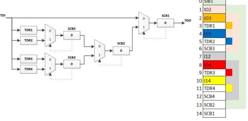
2.2.1 Hierarchy Array
Retargeting requires processing on the network model (ICL) for generating specific scan vectors. Thus the retargeting engine also proposed an on-chip version of ICL which is referred to as Hierarchy Array (H-Array). For example, figure 2.6 shows the H-Array representation of a reconfigurable scan network. The color on the right side of the table represents the network that is included if the same color is activated. For example,SIB1(green) will include the whole scan network when it is activated.
MeanwhileIO3 will only includeTDR1, etc.
2.2.2 Retargeting Engine Interface
Retargeting engine interacts with the IJTAG scan network, therefore it has IJTAG ports interface : SI,RST,Sel,CE,SE,UE,TCK andSO(figure 2.7). Other than the
IJTAG related ports, it has seven other ports. Those seven ports comprise of : 1. RegValue: provide the value for a register (instrument);
2. RegID: provide the value of register ID corresponding to the register index in the H-Array;
3. Concurrent: define the concurrent group of commands;
4. Read/Write: define the read or write of an access request (1 for read, 0 for write); 5. ReadID : return the read ID of a register corresponding to the register index in the H-Array;
6. ReadValue: return the read value of a register (instrument); 7. Error : Return an alert if an error occurs;
2.2. RETARGETINGENGINE 11
2.2.3 How Retargeting Engine Works
Retargeting engine works by first receiving access requests for one or more registers (instruments). Each access request needs to provide the operations (write or read) onRead/Writeport, register value (used for write value) onRegValueport and
regis-ter ID (correspond to H-Array) onRegID port. Retargeting engine executes a group
of access requests concurrently. A group of access requests is formed while the
Concurrent port stays HIGH. So several access requests that are requested while
theConcurrent port HIGH are considered to be in the same group. After a group of
access requests is formed and Concurrent port goes LOW, the retargeting engine
starts to generate scan vectors for the access requests. Finally, the retargeting en-gine returns ReadID and ReadValue if there are read access requests unordered,
because the retargeting engine produces effective scan vectors that may access embedded instruments not in order.
Figure 2.8: Example of a group of concurrent access requests
For example, figure 2.8 shows the waveform of a group of access requests for retargeting engine. This example uses the same H-Array that has shown before in figure 2.6. These access requests comprise of writing 0b0010 toTDR1, writing
0b1000 toTDR2, read from TDR2 and read fromTDR1, while theConcurrent port
stays HIGH. WhenConcurrent port goes to LOW, retargeting engine interprets it as
the end of a group of access requests and starts to generate scan vectors for these access requests. Since the returning of read access requests are unordered, it is possible to get the value ofTDR1first followed byTDR2 although the orders are the
2.3 Compiler
Compiler is a computer program that reads a program written in one language (source language) and translates it into another language (target language) [1] (fig-ure 2.9). The target language of a compiler is generally a machine executable language (machine code). The first complete compiler was implemented by John Backus who compiled FORTRAN into IBM 704 computer in 1957.
Figure 2.9: Compiler [1]
2.3.1 Compiler Phases
As a translator from source language into another language, a compiler works in several phases. Alfred Aho in the infamous dragon book [1], defined six phases of
a compiler. It consists of :
1. Lexical Analyzer : Reads the characters in the source program and returns stream of tokens;
2. Syntax Analyzer : Imposes hierarchical structure on the token stream;
3. Semantic Analyzer : Ensures the declarations and statements are semanti-cally correct;
4. Intermediate Code Generator : Generates intermediate representations of the source program (optional);
5. Code Optimizer: Improves the source-represented code in order to produce faster machine code (optional);
6. Code Generator: Generates target code.
For example, a program that counts a position from initial position and rate is
shown in figure 2.10. Lexical Analyzer changes the position, initial and rate into
id1, id2 andid3 respectively. Then the Syntax Analyzer produces the correct parse
tree and the Semantic Analyzer fills the parse tree with correct types. Next the Intermediate Code Generator generates intermediate representations of the parse
tree. Furthermore, the Code Optimizer improves the intermediate representations
2.4. CROSSCOMPILER 13
Figure 2.10: Example of phases in compiling a program [1]
2.4 Cross Compiler
[image:29.595.96.530.87.320.2]Cross compiler is a compiler that can generate a machine code for another platform other than the platform where the compiler is running [10]. This approach is used to compile a machine code for a platform that is not capable to run a compiler for itself. The history of cross compiler dated back in 1979 when it was impossible to compile ALGOL 68 to Z80 CPU due to insufficient memory. Then ALGOL 68 code was compiled in other platform to generate ZCODE for Z80 CPU.
Chapter 3
Analysis of HW-SW Co-Design
[image:31.595.228.395.415.737.2]An on-chip IJTAG dependability processor is a dedicated processor for executing a dependability application. While executing a dependability application, the proces-sor needs to access embedded instruments on the IJTAG network. This makes the on-chip IJTAG dependability processor falls into Application-Specific Instruction set Processor (ASIP) category. Hence, ASIP design methodology [2] is required as a framework to design an on-chip IJTAG dependability processor from hardware and software sides.
Figure 3.1: ASIP Design Methodology [2]
The input of ASIP design methodology is an application and the design con-straints. The application is a dependability application written in PDL. Section 2.1.2 explained that PDL consists of PDL level 0 and 1, hence PDL level 1 extends Tcl scripting language that enables what programming languages can do such as math-ematical and logical operations along with branches, loops, statements, etc. This thesis will implements all PDL operations in PDL level 1 to be able to execute what programming languages can do. Within PDL there are several commands that in-stantiate retargeting. Thus, there is a previous work that proposed an on-chip retar-geting which is referred to as retarretar-geting engine [9]. Hence the design requirements of an on-chip IJTAG dependability processor comprise of : enable to execute PDL and re-use the retargeting engine as a co-processor. As for design constraints, since the on-chip IJTAG dependability processor is a dependability system of an SoC, it must be very reliable. Such condition can be achieved by having a simple processor as possible that has lower probability of malfunctioning transistors.
ASIP design methodology comprises of 4 steps that cover :
1. Application Analysis: Analyze what kind of application that the processor can do.
2. Architectural Design : Explore possible architectures using step 1 as the given design constraints.
3. Instruction Set Generation : Generates instruction sets for an on-chip IJTAG dependability processor.
4. Software and Hardware Synthesis : Machine code generator and processor design.
This chapter explains the first 3 steps, meanwhile the hardware synthesis and software synthesis will be discussed in the next chapter as hardware and software implementations.
3.1 Application Analysis
In this thesis PDL becomes an important part because it is used to write the depend-ability application. PDL level 1 as an extension of Tcl sciprting language can be used to define mathematical and logical operations, along with expressions, statements, procedure calls, branches, etc. Hence in order to execute PDL, at least the hard-ware and softhard-ware parts of an on-chip IJTAG dependability processor needs to be able to provide those operations.
3.1. APPLICATIONANALYSIS 17
Table 3.1: PDL commands [7]
Command Purpose
iPDLLevel Identify PDL level
iPrefix Specify hierarchical prefix
iReset Reset the network
iWrite Queue data to be written iRead Queue data to be read iScan Queue data to be scanned
iOverrideScanInterface Indicate the capture, update and broadcast behavior to be im-posed on a list of scan interfaces
iApply Execute queued operations
iClock Specify a system clock which is required to be running
iClockOverride Override definition of system clock when it is generated on-chip iRunLoop Issue a number of clocks
iProc Wrapper for a PDL
iCall invoke a PDL procedure
iProcsForModule Identify the module in the ICL with which subsequent iProcs are associated
iUseProcNameSpace Use namespace for subsequent iCalls iNote Send text to runtime
iMerge Allow merging of iCalls
iTake Disallow other merge threads from modifying a model resource iRelease Re-allow other merge threads to modify a model resource iState Document the current state of the network
iGetReadData Return the value from most recently applied iRead operation iGetMiscompares Return the XOR of the value from most recently applied iRead
operation
iGetStatus Return the decimal number of iApply miscompares that have oc-cured since the last time iGetStatus was issued
iSetFail Return the message string to the controlling program to indicate an unexpected condition
From those 7 commands iRunLoop, iGetReadData and iPDLLevel commands are only able to be executed in the software side. In the implementation of iRunLoop, it can instantiate No Operation (NOP) instructions to make a waiting state until the required time is fulfilled (explaied later in section 5.6). iGetReadData command only enables the data that has just been fetched for further processing, this can be implemented by moving the data from the retargeting engine into main processor. Finally iPDLLevel does not need any instructions, this can be done in compiler level to check whether the PDL level is correct. Nonetheless iReset, iWrite, iRead and iApply require serious software implementations, but these commands also require to be generated as instructions in the hardware side. Because these commands interact with the retargeting engine directly.
Table 3.2: Implementation of PDL commands Command Implemented in
iPDLLevel SW
iReset SW-HW
iWrite SW-HW
iRead SW-HW
iApply SW-HW
iRunLoop SW
iGetReadData SW
Meanwhile, the other 17 PDL commands are not going to be implemented in this thesis with specific reasons. iPrefix, iUseProcNameSpace, iProcsForModule, and iProc commands are not necessary because the retargeting engine substitutes the ICL with H-Array, this also affects on the implementation of iCall command since iProc command is not implemented. iOverrideScanInterface and iState commands are optional because overriding and documentation are not fundamental. iTake, iMerge and iRelease commands enable threading for parallel processing, these commands are optional for improving the performance later. iClock and iClockOver-ride commands are not necessary to be implemented, because this thesis assumes to only have one clock source, the system clock. iScan is not implemented be-cause it behaves similar to iWrite and iRead but in more detail, thus iScan can be substitued with iWrite and iRead commands. Finally, iNote, iGetStatus, iGetMiscom-pares and iSetFail commands behave as notification system for the user which are not applicable since an on-chip IJTAG dependability is an embedded processor.
Thereby, the requirements to execute PDL comprise of :
3.2. ARCHITECTURALDESIGN 19
2. Being able to perform iReset, iRead, iWrite and iApply commands for retargeting engine co-processor.
3. Being able to perform iRunLoop, iGetReadData and iPDLLevel commands in the software side.
3.2 Architectural Design
Architectural design explores possible architecture based on the requirements of : executing PDL and re-use retargeting engine as a co-processor. The requirements to execute PDL has been explained on section 3.1. There are many processor types that meet such requirements such as Intel, ARM, Power PC, LEON and MIPS processors. Thus most of it falls under proprietary rights that requires a license to produce, use and/or synthesize. Only the early generation of MIPS and LEON that is available.
The only constraint of an on-chip IJTAG dependability processor is the hard-ware design should be as simple as possible in terms of area. Compared to early generation of MIPS, LEON processor requires vast area which does not meet the constraint. Since the early generation of MIPS was developed in 1985, until now researchers around the world has explored several variants from the early genera-tion of MIPS, such as Mini MIPS [11], Fault tolerant MIPS [12] and Single cycle 32 bits MIPS [5]. From these three options Single Cycle 32 bits MIPS offers the sim-plest architecture from the remaining options. Hence the design of an on-chip IJTAG dependability processor is based on the architecture of Single cycle 32 bits MIPS.
Single cycle 32 bits MIPS covers what general embedded processor can do. It can handle mathematical and logical operations, jumps, branches, load and store. Statements are done by assigning a value to a register, while loops and procedure calls are handled by performing jumps into a specific address. Single cycle 32 bits MIPS is also able to integrate retargeting engine as a co-processor by following MIPS specification [4]. This section will explains the analysis of how single cycle 32 bits MIPS can meet the design requirements without violating the constraint.
3.2.1 Fixed Point Representation
technology shows that FPU is 70 % larger than the whole single cycle 32 bits MIPS processor (Table 3.3). It is clear that integrating FPU is not an option for the sake of simplicity. Hence there is another option for a processor without FPU to calculate real numbers by changing the number representation into fixed point in the software side.
Table 3.3: Area comparison Single Cycle 32 bits MIPS & FPU
Hardware Areaµ2
Single Cycle 32 bits MIPS 193551.73
FPU [13] 331635.98
3.2.2 Software Emulated Operations
Arithmatic Logic Unit (ALU) is a digital circuit that can perform mathematical and logical operations. It is the main building block of a processor. The ALU of modern processors can perform complex mathematical and logical operations. In this case, it can process complex operations extremely fast. However it consumes enormous areas than a simple ALU that can only do add and shift operations.
Table 3.4: Single cycle 32 bits MIPS ALU support [5]
3.3. INSTRUCTIONSETGENERATION 21
32 bits MIPS. And the second approach is to emulate those required operations in the software side.
Multiplication and division are complex operations. Multiplication hardware com-prises of adders and shift registers. Divider hardware is even more complex than multiplication hardware, because it needs to handle exclusive cases such as divi-sion by zero and remainders. The main reason to use single cycle 32 bits MIPS processor is that it offers the simplest processor for the hardware of dependability system. Therefore, the second option is preferable, multiplication and division op-erations will be emulated in the software side. This solution also applies for other complex operations that are required such as square root and power.
3.3 Instruction Set Generation
Instruction set connects the hardware and the software sides. The software side compiles a PDL file into a set of instructions and the hardware side executes this set of instructions. This thesis uses MIPS instruction set from [3] [4]. However there are PDL requirements to generate iReset, iRead, iWrite and iApply commands into instructions that has been discussed in section 3.1 (table 3.2), therefore the MIPS instruction set needs to be extended. Before that, MIPS instruction set must be investigated first.
Majority of MIPS instructions fall into three categories: R-Type, I-Type and J-Type [3]. Register-J-Type (R-J-Type) instructions are used when all the data values are located in registers. Immediate-Type (I-Type) instructions are used when the instruc-tions must operate with an immediate value. Finally Jump-Type (J-Type) instrucinstruc-tions are used to perform a jump to an address.
Figure 3.2:MIPS instruction formats [3]
Each instruction type has its own instruction format (figure 3.2). All instructions have an opcode part on the first 6 bits of its most significant bits, where the rest
may differ for each type. With Register Destination (RD), Register Source (RS)
simultaneously for its operations. The R-Type instructions also have a shif t part
for shifting amount and a f unct part for defining the function for its operations. On
the other side, I-Type allocates its least significant 16 bits to an immediate value. Meanwhile, J-Type allocates its least significant 26 bits outside of opcodefor a jump
address.
Figure 3.3: MIPS Co-Processor Type Instruction Formats [4]
Outside of R, I and J-types, MIPS processors also support another type that is co-processor instructions. These instructions enable MIPS main processor to command its co-processors and exchange data between them [4]. The opcode
of processor type is ’0100XX’ where the last two bits refer to a specific co-processor (figure 3.3). The format of co-co-processor type instructions depend on its co-processor. For example, figure 3.4 depicts how Move From Co-Processor (MFC) instructions for co-processor 0, 1 and 2 have different formats. MFC0 moves a data to register RT in the main processor from register RD in co-processor 0 with
spe-cificsel. MFC1 also moves a data to registerRT in the main processor from register F S in co-processor 1, this data movement is used between MIPS processor with
FPU co-processor. Nonetheless, MFC2 moves a data to register RT in the main
processor, but the implementation part in the co-processor side depends on the
co-processor designer to implement it.
Figure 3.4:MFCX instruction formats [4]
3.3. INSTRUCTIONSETGENERATION 23
general MIPS architectures that employ co-Processor 0 and 1. Since retargeting en-gine enables write and read into an the IJTAG network, it needs to be able to move data to and from the co-processor. From co-processor point of view there are two sources/destinations for data movements which are main processor and memory (figure 3.5). Move a data from co-processor to MIPS processor can be handled with MFC instruction and move a data to co-processor from MIPS processor can be han-dled with Move To Co-Processor (MTC) instruction. For data movements between memory and co-processor, Store Word Processor (SWC) and Load Word Co-Processor (LWC) instructions can be used to store and load the data respectively. In the co-processor side, a register file will be added to hold the data and to ease data movements.
Figure 3.5:Co-Processor Data Movement
Figure 3.6: Mapping iWRITE instruction to retargeting engine
To fulfil PDL requirements the hardware needs to generate iWrite, iRead, iAp-ply and iReset PDL commands into MIPS instructions. As explained in section 2.2, retargeting engine requires two data (RegID and RegValue) to process an iWrite
Figure 3.7: Mapping iREAD instruction to retargeting engine
which can be placed inRT andRD becauseRS has been reserved forspecial part
(figure 3.3). In the instruction format, iWRITE instruction takes the usual place of
RT and RD for representing RegID and RegValue (figure 3.6). Meanwhile iRead
command only requires one data (RegID), so the iREAD instruction can take usual
place of RT for representing RegID (figure 3.7). Finally iApply and iReset
com-mands need no data, so iAPPLY and iRESET instructions can be implemented by
opcode and special only. Although generating iAPPLY instruction is just simply add
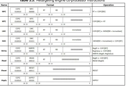
a new instruction, but the real work is in the software side that will be explained in section 5.6. Table 3.5 shows the instructions along with its formats and operations for retargeting engine co-processor.
3.4. DISCUSSION 25
3.4 Discussion
This chapter describes the analysis of hardware and software co-design of an on-chip IJTAG dependability processor. It uses ASIP design methodology [2] that com-prises of 4 steps : Application Analysis, Architectural Design, Instruction Set Gener-ation and Software-Hardware Synthesis. This chapter only covers the first 3 steps and leaves the last step for the implementation chapters later.
The input of ASIP design methodology is application and design constraints. In this thesis the application is a dependability application that is written in PDL. PDL has two levels 0 and 1. PDL level 1 is developed as an extension of Tcl that can be used to define mathematical and logical operations, expressions, statements, procedure calls and branches. This thesis treats all PDL commands as PDL level 1. Within PDL there are several commands that instantiate retargeting. Thus, there is a previous work that proposed an on-chip retargeting referred to as retargeting engine [9]. Hence the design requirements of an on-chip IJTAG dependability processor are : executing PDL and re-use the retargeting engine as a co-processor. There is only one design constraint which is the hardware design must be very reliable, such condition can be achieved by having a simple processor as possible that has lower probability of malfunctioning transistors.
On the Application Analysis step, the requirements for PDL is explained. Since dependability application is written in PDL, it inherits what PDL can provide. PDL level 1 as an extension of Tcl can be used to define mathematical and logical op-erations, expressions, statements, procedure calls and branches. Moreover PDL has 24 PDL commands (not part of Tcl) that are IJTAG related. This thesis only implements 7 commands which are fundamental to use IJTAG : iWrite, iRead, iAp-ply, iReset, iRunLoop, iPDLLevel and iGetReadData commands. Hence only iWrite, iRead, iApply and iReset commands that will be generated into instructions because it will interact directly with the retargeting engine.
On the Architectural Design step, single cycle 32 bits MIPS processor is cho-sen as the base of an on-chip IJTAG dependability processor, because single cycle 32 bits MIPS processor offers the simplest and open source processor architec-ture. To meet the design constraints which are having a simple hardware design, co-processor 0 and 1 are not included. Hence, real number operations will be com-pensated in the software side. Complex arithmetic operations such as division, mul-tiplication, power and square root are not implemented in the ALU, but it will be emulated in the software side as well to keep the hardware design as simple as possible.
mathematical, logical, jumps, branches and what common processor can do. The requirement for re-using retargeting engine co-processor also requires instruction set design. First the retargeting engine is placed in co-processor 2 so that it does not alter general MIPS architectures. Then it is followed with generating iWrite, iRead, iApply and iReset commands as MIPS co-processor type instructions for IJ-TAG related operations. Finally other co-processor instructions are added for data movement from and to co-processor such as MFC, MTC, SWC and LWC instruc-tions.
From those ASIP design methodology, hardware and software design require-ments can be concluded. Hardware design requirerequire-ments comprise of :
1. Implement retargeting engine as MIPS co-processor
2. Implement the co-Processor type instructions for retargeting engine co-processor.
Software design requirements comprise of :
1. Enable to translate PDL syntaxes into MIPS machine code 2. Map PDL commands into co-processor type instructions 3. Use fixed point representation
4. Compensate complex hardware operations by emulating multiplication, division, square root and power operations in the software side.
Chapter 4
IJTAG Dependability Processor
As explained in chapter 3, the hardware side of an on-chip IJTAG dependability pro-cessor design based on a single cycle 32 bits MIPS [5]. The analysis on that chapter produces hardware requirements to extend the design of a single cycle 32 bits MIPS to :
1. Implement retargeting engine as MIPS co-processor
2. Implement the co-Processor type instructions for retargeting engine co-processor.
This chapter explains how the initial design of single cycle 32 bits MIPS is ex-tended to achieve those previous hardware requirements. It starts with brief expla-nation about a single cycle 32 bits MIPS. Then it is followed by hardware design and is closed with a discussion. The result of this chapter is a hardware design of an on-chip IJTAG dependability processor.
4.1 Single Cycle 32-bits MIPS
MIPS stands for Microprocessor without Interlocked Pipeline Stages. The research of MIPS was started in 1981, led by John L. Hennessy. It yielded the first MIPS pro-cessor in 1985. Nowadays, the first generation of MIPS becomes the most studied processor that can be accessed easily in [3]. This ignites researchers around the world to investigate and produce many variants of first generation MIPS, such as Mini MIPS [11], Fault tolerant MIPS [12] and Single cycle 32 bits MIPS [5].
4.1.1 MIPS Stages
MIPS is a Reduced Instruction Set Computer (RISC) that suits for general proces-sor. There are 5 operations that each instruction holds which are : Instruction Fetch (IF); Instruction Decode (ID); Execute (EX); Memory Access (MEM); and Write
Figure 4.1: MIPS stages [3]
Back(WB). Those stages are done in pipeline manner (figure 4.1). On the orange highlighted clock cycle, MIPS processor executes WB for instruction 1, MEM for instruction 2, EX for instruction 3, ID for instruction 4 and IF for instruction 5.
Single ccle 32 bits MIPS processor is a 32 bits RISC processor that preceded modern MIPS architectures. Single cycle 32 bits MIPS executes all five stages (IF, ID, EX, MEM and WB) in a single clock cycle (figure 4.2). In return, this architecture can not work in high frequency clock.
Figure 4.2: Single Cycle MIPS stage [5]
4.1.2 MIPS Register
MIPS processor has 32 general purpose registers. These registers are placed in a register file. MIPS assembly language employs a convention for use of registers. This convention must be followed by MIPS assembly language programmers in order to avoid unexpected behaviours of module that is written by different people. These 32 general purposes registers has its own usage [8] (table 4.1). Register$0is
hard-wired into 0 and is not allowed for holding data. Register$atis a temporary register
that its use is limited to assembler. Register $v0 and $v1 are used to hold return
4.1. SINGLECYCLE32-BITSMIPS 29
calls subprograms. Register $s0 - $s7 are saved registers that is preserved when
MIPS processor calls subprograms. Register $k0 and $k1 are reserved by kernel
and are restricted to use. Finally register $gp, $sp, $f p and$ra are used for global
[image:45.595.92.538.202.438.2]pointer, stack pointer, frame pointer and return address respectively.
Table 4.1: MIPS register [8]
Register Number Conventional Name Usage
$0 $zero Hard-wired to 0
$1 $at Assembler temporary
$2-$3 $v0,$v1 Return values from functions $4-$7 $a0 -$a3 Arguments to functions
$8-$15 $t0 -$t7 Temporary registers, not preserved by subprograms $16-$23 $s0 -$s7 Saved registers, preserved by subprogram
$24-$25 $t8,$t9 More temporary data, not preserved by subprograms $26-$27 $k0,$k1 Reserved by kernel. Do not use
$28 $gp Global pointer
$29 $sp Stack pointer
$30 $fp Frame pointer
$31 $ra Return address
4.1.3 MIPS Co-Processor
MIPS R2000, the first generation of MIPS, is able to embed four co-processors. This specification is still preserved until the latest model of MIPS architectures [4]. The first two co-processors have been reserved in MIPS architectures (figure 4.3). Co-Processor 0 handles traps, exceptions, interrupt service routines and virtual mem-ory. Meanwhile, co-Processor 1 handles floating point operations. This configuration leaves two more slots to put co-processors in it.
MIPS co-processors may have a register file in it. There are no strict naming convention for register file for co-processors. Hence this thesis will use the common register naming that is generally used in MIPS reference [4]. MIPS reference [4] address a register in main processor with the conventional name that is shown in table 4.1. When addressing a register in co-processor, it starts with ’CPR’ followed by a bracket that consists of co-processor number and the register number. For example addressing register number 9 in co-processor 3 is written :
Figure 4.3: MIPS R2000 [3]
[image:46.595.151.419.81.402.2]4.2 Extending Single Cycle 32 bits MIPS
Figure 4.4: Single Cycle 32 Bits MIPS [5]
4.2. EXTENDINGSINGLECYCLE32 BITSMIPS 31
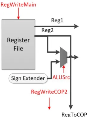
data movements are required from and to co-processor that employ MTC, MFC, SWC and LWC instructions. Also in section 3.3, it is known that RS part is used
for special, so the data can only be placed in RT and RD. Thus the input data to
co-processor comes from the output ofReg2, becauseReg2is connected toRT and RD. According to section 3.3, register file will be added into the retargeting engine
co-processor, hence it needs a control signal to enable write into register file in the co-processorRegW riteCOP2. So when an MTC2 instruction is executed the data
will pass the Reg2 into the co-processor 2 and RegW riteCOP2 signal needs to be
[image:47.595.239.384.256.450.2]active (figure 4.5).
Figure 4.5: Extending for MTC
Figure 4.6: Extending for MFC
[image:47.595.230.397.519.686.2]choose betweenW riteBack, the initial path for writing to register file in main
proces-sor, andCOP DataOut, the output of co-processor, with select signalCOP T oM ain.
So that when an MFC2 instruction is executed the data will pass the COP DataOut
intoRegW ritethat needs activeCOP T oM ainselect signal (figure 4.6).
Then when a data is stored from co-processor to data memory, it needs to be placed into the input data of the memory. Hence a multiplexer is required that can choose between Reg2, the initial path for writing to data memory in main processor,
and COP DataOut, the output of co-processor, with select signal COP T oM em. So
that when an SWC2 instruction is executed the data will pass theCOP DataOutinto
the input of data memory that needs activeCOP T oM emselect signal (figure 4.7).
Figure 4.7: Extending for SWC
Figure 4.8: Extending for LWC
Finally when a data is loaded to co-processor from data memory, it needs to be placed into the output data of the memory. M emT oReg select signal needs
4.2. EXTENDINGSINGLECYCLE32 BITSMIPS 33
single cycle 32 bits MIPS for MTC2, there is an input signal RegT oCOP that was
added before. So a multiplexer is required that can choose between RegT oCOP
andW riteBackwith select signalM ainT oCOP. So that when an LWC2 instruction
is executed the data will pass the W riteBack afterM emT oReg signal is active and
then it will pass toCOP DataInafter theM ainT oCOP signal is active. However this
operation needsRegW riteCOP2 signal to be activated too so that writing into the
co-processor register file is able (figure 4.7).
Lastly, since there are 4 new instructions that is dedicated for the retargeting engine co-processor (iWRITE, iREAD, iAPPLY and iRESET), theninstructionsignal
[image:49.595.189.438.286.723.2]needs to be connected into the retargeting engine co-processor as well. Figure 4.9 shows the diagram block of an on-chip IJTAG dependability processor hardware.
4.3 Retargeting Engine Wrapper Design
Retargeting is a compulsory operation in order to access embedded instruments on the IJTAG network. This thesis uses an on-chip retargeting engine that has been proposed by [9] for handling the on-chip retargeting. To embed the retargeting engine into a co-processor for single cycle 32 bits MIPS, the design of a wrapper for retargeting engine is required which will be placed in co-processor 2 as explained in section 3.3.
Section 2.2 explained that retargeting engine works by first receiving access re-quests to one or more instruments. Then it starts to work when theConcurrent
sig-nal is changed from HIGH to LOW. This condition is important to be considered in order to use the retargeting engine. According to section 3.3, these access requests are instructions. However due to theConcurrent signal condition, connecting the
re-targeting engine directly with the instructions is not possible. For example after the retargeting engine get an access request for writing 0b0010 toT DR3, the main
pro-cessor can not directly provide next access requests (figure 4.10). Because the main processor needs to move the data from main processor to co-processor (explained in section 3.3). On the other hand the retargeting engine has already interpreted it as a start to generate scan vectors due to the change in the concurrent signal (figure 4.10). To solve this problem, it is best to put an instruction buffer in the wrapper. In this manner the retargeting engine wrapper can send the buffered instruction as a group of concurrent instructions into the retargeting engine when iAPPLY instruction is received.
Figure 4.10:Concurrency problem on retargeting engine
When retargeting engine has finished accessing embedded instruments, retar-geting engine returnsReadIDandReadValueif there is an access request for
4.3. RETARGETINGENGINEWRAPPERDESIGN 35
Since the connection between instruments on the IJTAG network might be a com-plex connection, the retargeting engine will generate effective scan vectors for the access requests. However the results may return the data unordered, which in the example is depicted by the return values ofT DR3followed byT DR5(figure 4.11).
Figure 4.11: Retargeting Engine Returns Unordered Data
To solve the unordered returning values, the information in the instruction buffer can be used to arrange these unordered returning values. Moreover in section 3.3 and 4.2, it has been discussed that a register file will be added to the retargeting engine co-processor precisely in the retargeting engine wrapper. Since the returning data will be used in the main processor later, it is better to place the data into the wrapper register file right away. Thus wrapper controller is required to check the returning values according to the instruction buffer and place the returning order in the register file (figure 4.12).
Figure 4.12: Arrange The Unordered Returning Values
controller for controlling the wrapper and arranging the unordered returning values into the wrapper register file.
Figure 4.13: Retargeting engine wrapper block diagram
Figure 4.14: Retargeting Engine wrapper flow chart
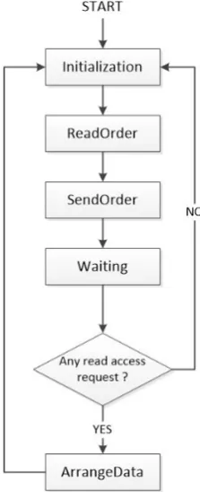
4.4 Retargeting Engine Wrapper Workflow
Consider the behavior of the retargeting engine, The works of retargeting engine wrapper comprise of several phase. Figure 4.14 shows the flow chart of retargeting engine wrapper, which are :
4.4. RETARGETINGENGINEWRAPPERWORKFLOW 37
2. ReadOrder: read an incoming order and put it to buffer,
3. SendOrder : send the buffered orders into retargeting engine, if iApply order is detected,
4. Waiting: wait the retargeting engine until it finishes accessing embedded instru-ments,
[image:53.595.98.532.232.587.2]5. ArrangeData : fetch and arrange the incoming data according to the instruction buffer into wrapper register file.
Figure 4.15:Reading an iWrite access request
Initializationphase resets the instruction buffer and prepares for reading access
requests from the incoming instructions in instruction port. While in ReadOrder
phase, the wrapper is ready to read access requests for specific instructions. For example figure 4.15 shows the steps of an access request for writing 0b0010 into
T DR3starts in PDL, machine code and hardware. It starts with the main processor
sends the RegID followed by RegValue and finally followed by an iWRITE
instruc-tion. ReadOrder phase ends when there is an iAPPLY command, then it changes
re-targeting engine, in this way access requests can be send concurrently. After all the instructions in the instruction buffer was sent, the wrapper waits until the retargeting engine finishes accessing the embedded instruments in the Waiting phase. When
the retargeting engine has finished, if there is no access request for reading, the wrapper goes to the Initialization phase and sets register 1 in wrapper register file
to 1 as an acknowledge signal. However, if there is an access request for reading, the wrapper goes to the ArrangeData phase. ArrangeData phase reads the
incom-ing data and arranges it accordincom-ing to the instruction buffer into wrapper register file as explained in section 4.3 and sets register 1 in wrapper register file to 1 as an acknowledge signal.
Other than iWRITE instruction, the hardware requirements also requires the re-targeting engine co-processor to be able to execute iREAD, iRESET and iAPPLY. Ex-ecuting iREAD instruction is similar to exEx-ecuting iWRITE instruction but without Reg-Value. On the other hand, executing an iRESET instruction is done by forcing the RST port to HIGH in the output of retargeting engine wrapper port. Finally
execut-ing an iAPPLY instruction is done by providexecut-ing a flag for retargetexecut-ing engine wrapper controller to start sending order into the retargeting engine. It has been explained in section 2.1.2 that accessing embedded instruments take non-deterministic of time. In the hardware side this non-deterministic is handled by Waiting phase in wrapper
controller, so that the software side also needs to handle this condition too.
4.5 Discussion
In this chapter, the hardware design of an on-chip IJTAG dependability processor has been explained. The design based on single cycle 32 bits MIPS that has been described in chapter 3. The hardware design aims to achieve the hardware require-ments which are implement retargeting engine processor and implement the co-processor type instructions for retargeting engine co-co-processor. The hardware de-sign starts by extending the single cycle 32 bits MIPS to enable data movements MFC2, MTC2, SWC2 and LWC2 instructions. Then it is followed by enabling the iWRITE, iREAD, iRESET and iAPPLY in the retargeting engine co-processor.
Retargeting engine process a group of concurrent instructions. Thus it is not suitable to connect the retargeting engine into decoded instructions directly, con-sequently a wrapper design for retargeting engine is required. To make sure the concurrency is preserved, instruction buffer is necessary to queue the instructions before it goes into the retargeting engine. When the retargeting engine finishes ac-cessing embedded instruments, it will returnReadValue andReadID unordered as
4.5. DISCUSSION 39
can be placed in wrapper register file that has been explained in section 3.3. The hardware of retargeting engine wrapper comprises of a register file, an instruction buffer, a wrapper controller and a retargeting engine.
Chapter 5
PDL Cross Compiler
Chapter 3 analyzes the hardware and software co-design for an on-chip IJTAG de-pendability processor. The results are hardware and software design requirements. This chapter focus on building a PDL cross compiler to achieve the software require-ments, which are :
1. Enable to translate PDL syntaxes into MIPS machine code 2. Map PDL commands into co-processor type instructions 3. Use fixed point representation
4. Compensate complex hardware operations by emulating multiplication, division, square root and power operations in the software side.
PDL cross compiler compiles PDL scripting language into a machine code, which in this thesis focus on MIPS machine code only. Building a PDL cross compiler starts with an analysis on how to build a cross compiler for PDL. Then it is followed with a brief explanation about ANTLR tool that is used as compiler framework while building a PDL cross compiler. Afterwards it describes PDL cross compiler design and is closed with a discussion. Additional section is added for explaining how to use the PDL cross compiler. The result of this chapter is software design of a PDL cross compiler.
5.1 Analysis on Building PDL Cross Compiler
PDL cross compiler translates a PDL program into MIPS machine code. According to section 3.1, this thesis considers all PDL operations to be PDL level 1 which extends Tcl scripting language. Tcl scripting language is designed to be interpreted than to be compiled. An interpreter directly executes the operations specified in the source program on inputs supplied by the user [1]. Thus the fundamental difference is interpreter does not produce a machine code. On the other hand a compiler takes

![Figure 3.1: ASIP Design Methodology [2]](https://thumb-us.123doks.com/thumbv2/123dok_us/9808836.482104/31.595.228.395.415.737/figure-asip-design-methodology.webp)
![Table 3.1: PDL commands [7]](https://thumb-us.123doks.com/thumbv2/123dok_us/9808836.482104/33.595.109.530.103.626/table-pdl-commands.webp)
![Table 4.1: MIPS register [8]](https://thumb-us.123doks.com/thumbv2/123dok_us/9808836.482104/45.595.92.538.202.438/table-mips-register.webp)
![Figure 4.4: Single Cycle 32 Bits MIPS [5]](https://thumb-us.123doks.com/thumbv2/123dok_us/9808836.482104/46.595.151.419.81.402/figure-single-cycle-bits-mips.webp)