An Efficient Implementation of Low Power
Three Input Xor/Xnor Gate
*K.SNEHA **Mr.U.VENU ***Mr.G.BABU
*M.TECH Dept of ECE,VAAGDEVI COLLEGE OF ENGINEERING
**Asst. prof Dept of ECE, VAAGDEVI COLLEGE OF ENGINEERING
***Asso. prof Dept of ECE, VAAGDEVI COLLEGE OF ENGINEERING
Abstract:
In this paper, we propose a new three input
XOR/XNOR circuit to reduce the delay and
power consumption as these circuits is basic
building blocks of many arithmetic circuits.
This paper evaluates and compares the
performance of various XOR-XNOR
circuits. We start with selecting a basic cell
including three independent inputs and two
complementary outputs. Next we combine
this basic cell with various correction and
optimization techniques to build a perfect
XOR-XNOR circuit with full swing
operation. The performance of the
XOR-XNOR circuits based on systematic cell
design methodology process models at all
range of the supply voltage is evaluated by
the comparison of the simulation results
obtained from MICRO WIND. The
simulation results demonstrate that the
proposed circuits are superior in terms of
speed, power consumption and power-delay
product (PDP) with respect to other designs.
I.INTRODUCTION
While the growth of the electronics
market has driven the VLSI industry
towards very high integration density and
GHz operating frequencies, critical concerns
have been arising to the severe increase in
power consumption and the need to further
reduce it. Moreover, with the explosive
growth demand and popularity of portable
electronics is driving designers to strive for
smaller silicon area, higher speed,longer
battery life, and more reliability. Power is
one of the premium resources a designer
tries to save when designing a system. The
XOR-XNOR circuits are basic building
blocks in various circuit
especially-Arithmetic circuits (Full adder, and
multipliers), Compressors, Comparators,
Parity Checkers, Code converters,
Error-detecting or Error-correcting codes, and
Phase detector circuit in PLL. We focus on
XOR–XNOR circuits as they are often used
to obtain optimized performances for full
adders. Balanced XOR–XNOR circuits
along with multiplexers are also the main
components of compressors in parallel
multiplication circuits. Also these circuits
play an important role in comparator and
parity checker blocks. Balanced XOR–
XNOR circuits, which serve as critical
components in balanced complimentary
outputs, eliminate power dissipated by the
glitches. In any type of logic design, the non
full swing outputs play a decisive role in cell
weak drivability. Full swing outputs impact
multi-stage structured arithmetic circuit
performance. Therefore designers consider
achieving full swing output operations as an
important factor in arithmetic circuit basic
block design.
The performance of the complex
logic circuits is affected by the individual
performance of the XOR-XNOR circuits
that are included in them [1]-[6].Therefore,
careful design and analysis is required for
XOR-XNOR circuits to obtained –full
output voltage swing, lesser power
consumption and delay in the critical path.
Additionally, the design should have a lesser
number of transistors to implement
XOR-XNOR circuits and simultaneous generation
of the two non-skewed outputs. In this paper
a PTL based XOR and XNOR circuits were
considers. Despite the saving in transistor
count, the output voltage level is degraded at
certain input combinations. The reduction in
voltage swing, on one hand, is beneficial to
power consumption. On the other hand, this
may lead to slow switching in the case of
cascaded operation. We propose and
compare new XORXNOR circuit designs
simultaneously with full output voltage
swing. The NMOS and PMOS transistors
are added to the basic circuits to alleviate the
threshold voltage loss problem commonly
encountered in pass transistor logic design.
We see many published papers that compete
in designing better circuits [7]- [12]. Such
studies mostly rely on creative design ideas
but do not follow a systematic approach. As
a
consequence, most of them suffer from
some different disadvantages [8].
1) They are implemented with logic styles
that have an incomplete voltage swing in
some internal nodes, which leads to static
power dissipation.
2) Most of them suffer from severe output
signal degradation and cannot sustain low
voltage operation.
3) They predominantly have dynamic power
consumption for non balanced propagation
delay inside and outside circuits, which
results in glitches at the outputs.
Therefore, a well-organized design
methodology can be regarded as a strong
solution for the challenge. Cell design
methodology (CDM) has been presented to
design some limited functions, such as
two-input XOR/XNOR and carry–inverse carry
in the hybrid-CMOS style [13]–[15]. The
predominant results persuade us to improve
CDM through two stages: 1) generating
more complex functions and 2) rectifying
some remaining flaws. The flaws in
previously published CDM include
containing some manual steps in the design
flow and generating a large number of
designs in which the predominant ones
would be determined after the completion of
simulations. CDM is matured as systematic
CDM (SCDM) in designing the three-input
XOR/XNORs for the first time. It
systematically generates elementary basic
cell (EBC) using binary decision diagram
(BDD), and wisely chooses circuit
components based on a specific target.
Therefore, after the systematic generation,
the SCDM considers circuit optimization
based on our target in three steps: 1) wise
selection of the basic cell; 2) wise selection
of the amend mechanisms; and 3) transistor
sizing. We consider the power-delay product
(PDP) as the design target. This method has
some advantages.
1. It increases the driving capability and
avoids the degradation on the output
2. It uses only less number of transistors in
the critical path which results in less delay
and power- delay product(PDP).
3. The dynamic consumption optimization
comes from the fact of well-balanced
propagation delay.
4. Power-ground-free main structure leads to
power reduction.
5. The methodology has high flexibility in
target and systematically consider it in the
three design steps. This can lead to efficient
circuits in terms of performance, power,
PDP, EDP, area, or a combination of them.
II.EXISTING WORK
In this section, we will see the
three-input XOR/XNOR circuits to examine their
high performance[ 16]. In complementary
CMOS logic [16], the pull-down and pull-up
networks used in the circuit perform the
function in a complementary way. It has
high noise margin and no static power
consumption. In the CMOS with
transmission gate ,[16]there is a advantage
of using less number of transistors. In
complementary pass-transistor, it has a good
output driving capability and pass-transistor
logics gain their speed over the CMOS due
to their high logic functionality.
The XNOR-XOR circuit by using
CMOS transistor and compare it with the
proposed design of XNOR-XOR circuit
using transmission gate with CMOS inverter
circuit. Figure-1[16] shows the XNORXOR
combine gate using CMOS transistor circuit.
There are total sixteen transistors used in
which 8transistors are PMOS and rest are
the NMOS transistors. The NMOS transistor
can give the “LOW” signal completely, but
it has very poor performance at “HIGH”
signal. Similarly PMOS transistor can gives
the “HIGH” signal completely, but poor
performance at “LOW” signal .
The concept of transmission gates
and CMOS inverter[17]. The CMOS
inverter is driving the transmission gate to
achieve the perfect output voltage swing. P
and Q are given as the input of transmission
gates through CMOS inverter. Output of
transmission gates gives the XNOR output
and using an inverter we get the XOR
output. The transmission gate allows to
passes the signal through it, when the enable
signal of transmission gate is high. The
transmission gate has a n-channel device and
situated on the bottom of the p-channel
MOS. When zero signals apply to the enable
(i.e. en) pin the transmission gate is off, and
no signal is transferred through it. When
enable signal is asserted high, the input
signal appears to the output.
III. PROPOSED WORK
1. INTRODUCTION OF CELLS
In this section we introduce different
basic cells which are used as a basis for
designing various circuits. To pro-vide
better understanding we first introduce the
elementary structure, referred to as the
elementary basic cell.
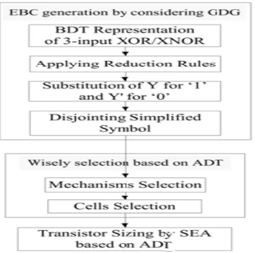
2. The Elementary Basic Cell
In order to generate the EBC of
three-input XOR/XNOR circuits, four steps
are taken. Initially, three-input XOR and its
complement is represented by one binary
decision tree (BDT) [18] in order to share
common sub circuits.
The step is followed by applying reduction
rules to simplify the BDT
representation[19]. These include
elimination, merging, and coupling rules.
The result of applied reduction rules to the
tree is shown in Fig. (c). as the inputs into
the first level are 0’s and 1’s of the
function’s truth table, the 0 and 1 can be
replaced by the Y and Y’ respectively. Then
the simplified symbol can be divided into
two distinct symbols: 1) the plus sign with
the x input control and 2) the minus sign
with the x‟ input control. The result of
applying steps 3 and 4 is shown in Fig.(d).
The EBC, which is extracted from the above
Fig a: SCDM process for designing efficient Fig b:BDT representation of three-input
Three-input XOR/XNOR XOR/XNOR function
Fig e: EBC
MECHANISMS
Different mechanisms are
optimization mechanisms to resolve non full
swing [inverter and feedback ],correction
mechanisms to resolve high impedance[pull
up-down network and feedback ], or the
combinations of them [bootstrap-pull
up-down, feedback pull up-up-down,
bootstrap-feedback , inverter bootstrap-feedback, and
inverter-pull up-down].
Introduction of Feedback Networks
All circuits with complementary
outputs have the ability to optionally
determine the state of an output or amplify it
through the use of another output and a
suitable transistor. Transistor or transistors
which are placed between the two outputs to
influence the second output through
activating the first one, are called feedback
networks. This feedback network is placed
between the two complementary out-puts
and causes the high impedance output states
to be eliminated and replaced by the desired
levels. Also, it is possible to ensure full
swing operation at the outputs. As different
basic cell versions presented in this work
come with different short comings, the
required feedback net-work should be
different.
We use four different feedback
networks and they are: Fp, Fn, Fc and Fnp.
Fp is a feedback network using two PMOS
transistors. Fn is a feedback network with
two NMOS transistors. Fc is a
complementary feedback network and Fnp
includes NMOS and PMOS transistors
placed between the two complementary