Compact Multilayer Hybrid Coupler Based
on Size Reduction Methods
Young Kim1, * and Youngchul Yoon2
Abstract—This paper presents a compact multilayer hybrid coupler based on a microstrip via-transition and short transmission line with a capacitor on each side to reduce circuit size. The microstrip via-transition is connected to two microstrip lines in different layers to configure a sandwich structure. To reduce the passive component circuit size, the design method uses a microstrip via-transition and a short transmission line with capacitors on each side. To validate the microstrip via-transition and short transmission line with capacitor, a multilayer hybrid coupler is implemented at a center frequency of 2 GHz. The measured characteristics agreed well with the simulation results, and above 90% circuit-size reduction compared with conventional couplers was realized.
1. INTRODUCTION
The LTE system of modern wireless communication requires high-speed data processing and compact circuit size. To satisfy these industry demands, integration technologies have been developed, such as system on a chip (SOC) and MMIC etc. [1–3].
Many methods of vertical transitions in planar microwave circuits have been researched Vertical via-hole structures [4, 5] are most commonly used in integrated circuit designs. Because a via-hole transition has the characteristic of a low pass filter, design for high frequency is limited. Aperture-coupled transition [6, 7] can change the shape of an aperture or a microstrip terminal and obtain improved bandwidth, but it cannot be used as an appropriate design method. Finally, cavity-coupled transitions [8, 9] have been presented to transfer signals through several layers with a relatively narrower bandwidth.
In addition, various methods have been proposed to effectively reduce the size of the branch line hybrid couplers [10–17]. The size-reduction methods are T-mode approach using open stub with high-low impedance [10], artificial transmission lines [11], printed distributed capacitor [12], high-impedance transmission lines and interdigitated shunt capacitor [13], and coupled-line section [14], etc.
In this paper, we propose a multilayer compact hybrid coupler based on microstrip via-transition and short transmission line with a capacitor to realize circuit-size reduction. Because the conventional hybrid coupler consists of fourλ/4 transmission lines, its circuit-size reduction is limited. To reduce a
λ/4 transmission line, we use a multilayer sandwich configuration to connect the transmission line in different layers using a microstrip via-transition. In addition, because theλ/4 transmission line converts an arbitrary short-length transmission line using capacitors at both end side, the proposed component can be reduced more compared with the configuration presented in [18].
Figure 1 shows the multilayer sandwich configuration with a microstrip via-transition.
Received 28 October 2014, Accepted 13 December 2014, Scheduled 26 December 2014 * Corresponding author: Young Kim ([email protected]).
1 School of Electronic Engineering, Kumoh National Institute of Technology, 61 Daehak-ro, Gumi, Gyungbuk, Korea. 2Department
2. THEORY AND DESIGN
Figure 1 shows that the proposed sandwich configuration with a microstrip via-transition consists of two microstrip lines with the same width, a ground plane in the middle layer, via-holes to connect the two microstrip lines that exist in different layers, and a slot to separate the ground plane and via-hole. To realize good electrical performance of the sandwich configuration, the microstrip-via transition should operate with low loss, high return loss, and at a wide frequency bandwidth.
To obtain the desired transmission line performance using the microstrip-via transition, we sweep the slot size to realize optimum characteristics. In Figure 1, the microstrip-via transition has two parameters, via-hole diameter d and distance s between the via and ground, in order to satisfy the transmission line characteristics of low insertion loss and matching for sandwich configuration. The microstrip-via transition consists of a via-hole between two transmission lines on an epoxy PCB with dielectric constantεr= 4.3 and thicknessh= 0.787 mm. In this case, we fix the diameter of the via-hole to d= 0.4 mm and the sweep slot size to between 0.2 and 0.5 mm.
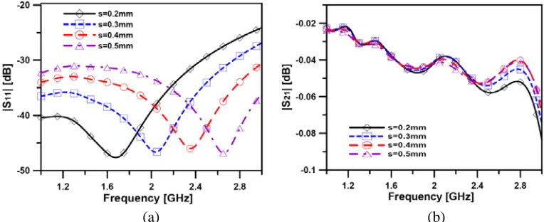
Figures 2(a) and (b) show theS-parameters of the slot size variation when the distance between the
Figure 1. Proposed sandwich configuration with a microstrip via-transition.
(a) (b)
Figure 2. S-parameters of the slot size variation in a sandwich configuration, (a)|S11|and (b) |S21|.
(a) (b)
via-holes and ground is varied froms= 0.2 mm tos= 0.5 mm. In addition, the sandwich configuration with a microstrip-via transition shows good performance at an operating frequency of 2 GHz. We design the via-hole diameter to d= 0.4 mm and the distance between the via-hole and ground tos= 0.3 mm to obtain an optimum transmission line with via-transition.
In addition, the circuit size reduction method uses a reduced-size transmission line (λg/4) with capacitors at both end sides. The λg/4 transmission line can be replaced by a transmission line of characteristic impedance Z and electrical length θ and shunt capacitances C at either end. Figure 3 shows the λg/4 transmission line and the equivalent circuit of a reduced-size transmission line with capacitors at both end sides. In Figure 3, the two circuit parameters become the same if the values of reduced size circuit parameterZ and C are chosen as follows:
Z = Zo
sinθ, ωC =
cosθ
Zo (1)
where Z is the impedance value of the reduced-size transmission line, C the shunt capacitance of the reduced-size transmission line, θthe electrical length of the reduced-size transmission line,Zo theλg/4 transmission line impedance value, λg the guided wavelength of design center frequency, and ω the angular frequency of design center frequency.
Because a conventional hybrid coupler has four λg/4 transmission lines with different impedance values, we designed a multilayer hybrid coupler with a sandwich configuration consisting of a transmission line and a short transmission line with capacitors at both end sides. This design uses Microwave Office from AWR Corporation.
3. SIMULATION AND EXPERIMENTAL RESULTS
To show the validity of the proposed compact multilayer hybrid coupler, we designed three hybrid couplers. In the first case, in order to show the validation of the microstrip-via transition and the reduction of circuit size, a 50-Ω λg/4 transmission line conventional hybrid coupler was converted into twoλg/8 transmission lines using microstrip via-holes with sandwich configuration. In the second case, in order to reduce the circuit size, both the transmission line of short electrical length ( λg/4) with shunt capacitances at either end and the microstrip-via transition are used. A 35-Ω λg/4 transmission line conventional hybrid coupler was converted into a 70-Ω transmission line with electrical length of 30◦ and both end-side capacitors had a capacitance value of 1.60 pF. The 50-Ω λg/4 transmission line conventional hybrid coupler was the same as that in the first case. Finally, in the third case, to design smaller than second case hybrid coupler, we are used a microstrip-via transition with reduced-size circuit method. A 50-Ω λg/4 transmission line conventional hybrid coupler was converted to a 70-Ω transmission line with an electrical length of 22.5◦ and both end-side capacitors had a capacitance value of 3.0 pF. The 35-Ωλg/4 transmission line of conventional hybrid coupler was the same as that in the second case. The simulation and fabrication were performed at a center frequency of 2 GHz. The compact multilayer hybrid coupler constituted the transmission lines using an epoxy substrate with
εr= 4.3 and thickness h= 0.787 mm.
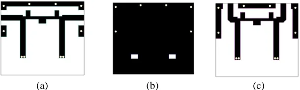
Figure 4 shows the top, middle and bottom PCB layouts of the multilayer hybrid coupler in the
(a) (b) (c)
second case. The top layer pattern is connected to the bottom layer transmission line pattern using a via-hole with a slot in the middle layer.
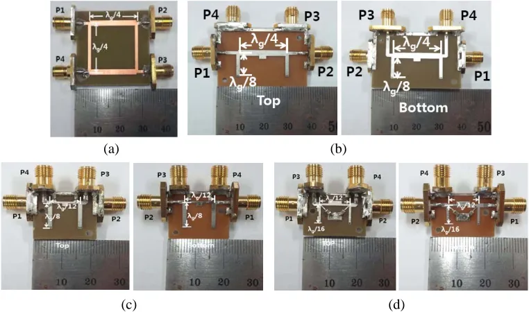
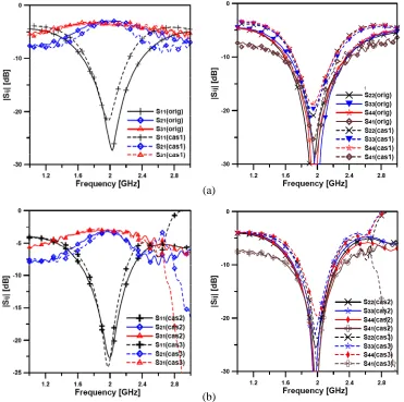
Figure 5 also shows the fabricated multilayer hybrid coupler for the three cases, in addition to the original hybrid coupler. The sizes of the hybrid couplers are as follows: original case (λg/4×λg/4), Case 1 (λg/4×λg/8) for only the transmission line with a sandwich configuration, Case 2 (λg/12×λg/8) for the mixed configuration with a small-section transmission line with capacitors at the end sides, and Case 3 (λg/12×λg/16) for only small section transmission line with sandwich configuration. λg represents the guided wavelength at 2 GHz with dielectric constant εr = 4.3. The figure shows that the circuit size is reduced to 50% in Case 1, 83% in Case 2, and 92% in Case 3 compared with the original hybrid coupler. Figure 6 shows the measured results. Table 1 lists the summary of the measuredS-parameters for the four cases. The data show that the characteristics of the four hybrid couplers under different design methods are the same. Table 2 shows the comparison of the reported branch-line hybrid coupler.
(a) (b)
(c) (d)
Figure 5. Top and bottom photographs of the implemented reduced size multilayer hybrid coupler. (a) Original. (b) Case 1. (c) Case 2. (d) Case 3.
Table 1. Summary of the measured S-parameters in the four cases at 2 GHz.
S11 (dB) S21 (dB) S31 (dB) S22 (dB) S33 (dB) S44 (dB) S41 (dB) Original −26.2 −2.95 −3.70 −24.2 −47.2 −29.6 −27.1
Case 1 −21.2 −3.21 −3.32 −19.2 −18.5 −17.6 −22.8 Case 2 −22.7 −3.36 −3.09 −24.8 −26.5 −35.1 −34.2 Case 3 −22.9 −3.19 −3.1 −23.8 −21.1 −19.6 −29.1
Table 2. Comparison of the reported branch-line hybrid coupler.
[10] [11] [12] [13] [14] This work
Frequency (GHz) 2.45 0.915 3.5 0.8365 0.9 2.0
Measured|S21|,|S31|(dB) 3.1/3.2 3.42/3.72 3±1 3.9±0.1 3±0.5 3.19/3.1
Isolation (dB) 36.2 40.0 35 28.9 40 29.1
Percentage of reduction 64.2 73 62 73.2 90.4 92
(a)
(b)
Figure 6. MeasuredS-parameters of the proposed compact multilayer hybrid coupler. (a)S-parameters of the original and Case 1 hybrid coupler. (b)S-parameters of Case 2 and Case 3 hybrid coupler.
4. CONCLUSION
This paper has presented a compact multilayer hybrid coupler with a transmission line with sandwich configuration and a small-section transmission line with end-side capacitors. Compared with the original hybrid coupler, the proposed hybrid coupler showed a maximum size reduction of 92%. The characteristics of the compact hybrid coupler remained the same. This design method can be used to reduce the component sizes of RF and microwave devices.
ACKNOWLEDGMENT
This paper was supported by Research Fund, Kumoh National Institute of Technology.
REFERENCES
1. Patti, R. S., “Three-dimensional integrated circuits and the future of system-on-chip designs,”
Proceeding of The IEEE, Vol. 94, No. 6, 1214–1224, Jun. 2006.
3. Kim, Y., S.-H. Sim, and Y.-C. Yoon, “Multilayer compact hybrid coupler based on vertical microstrip transition,” 2013 Asia-Pacific Microwave Conference Proceedings, 914–916, 2013. 4. Lopez-Berrocal, B., E. Marquez-Segura, I. Molina-Fernandez, and J. C. Gonzalez-Delgado, “A
circuit model for vertical multilayer transitions in coplanar waveguide technology,” Progress In Electromagnetics Research B, Vol. 41, 51–76, 2012.
5. Casares-Miranda, F., C. Viereck, C. Camacho-Penalosa, and C. Caloz, “Vertical microstrip transition for multilayer microwave circuits with decoupled passive and active layers,” IEEE Microw. Wireless Compon. Lett., Vol. 16, No. 7, 401–403, Jul. 2006.
6. Gauthier, G. P., J.-P. Raskin, L. P. B. Katehi, and G. M. Rebeiz, “A 94-GHz aperture-coupled micromachined microstrip antenna,” IEEE Trans. Antenn. Propag., Vol. 47, No. 12, 1761–1766, Dec. 1999.
7. Loffler, D., E. Gschwendtner, and W. Wiesbeck, “Apterture coupling versus connectors for the transition between T/R-modules and radiations in large phased arrays,”Antenna and Propagation Society International Symposium, Vol. 4, 2770–2773, Jul. 1999.
8. Lafond, O., M. Himdi, J. Danial, and N. Haese-Rolland, “Microstrip/thick-slot/microstrip transition in millimeter waves,” Microw. Opt. Technol. Lett., Vol. 34, No. 2, 100–103, Dec. 2003. 9. Swierezynski, T., D. McNamara, and M. Clenet, “Via-walled cavities as vertical transitions in
multilayer millimeter-wave circuits,” Electron. Lett., Vol. 39, No. 25, 1829–1831, Dec. 2003. 10. Elhiwaris, M. Y. O., S. K. A. Rahim, U. A. K. Okonkwo, and N. M. Jizat, “Miniaturized size branch
line coupler using open stubs with hig-low impedances,” Progress In Electromagnetics Research Letters, Vol. 23, 65–74, 2011.
11. Wang, C. W., T. G. Ma, and C. F. Yang, “Miniaturized branch-line coupler with harmonic suppression for RFID applications using artificial transmission lines,”IEEE/ MTT-S Inter. Dig., 29–32, 2007.
12. Jung, S. C., R. Negra, and F. M. Ghannouchi, “A design methodology for miniaturized 3-dB branch-line hybrid couplers using distributed capacitors printed in the inner area,”IEEE Trans. Microwave Theory &Tech., Vol. 56, No. 12, 2950–2953, Dec. 2008.
13. Tsai, K. Y., H. S. Yang, J. H. Chen, and Y. J. E. Chen, “A miniaturized 3 dB branch-line hybrid coupler with harmonics suppression,” IEEE Microw. Wireless Compon. Lett., Vol. 21, No. 10, 537–539, Oct. 2011.
14. Kim, J. and J. G. Yook, “A miniaturized 3 dB 90◦ hybrid coupler using coupled-line section with spurious rejection,”IEEE Microw. Wireless Compon. Lett., Vol. 24, No. 11, 766–768, Nov. 2014. 15. Eccleston, K. W. and S. H. M. Ong, “Compact planar microstripline branch-line and rat-race
couplers,”IEEE Trans. Microwave Theory & Tech., Vol. 51, No. 10, 2119–2125, Oct. 2003. 16. Tang, C. W. and M. G. Chen, “Synthesizing microstrip branch-line couplers with predetermined
compact size and bandwidth,”IEEE Trans. Microwave Theory &Tech., Vol. 55, No. 9, 1926–1934, Sep. 2007.
17. Wang, J., B. Z. Wang, Y. X. Guo, L. C. Ong, and S. Xiao, “A compact slow-wave microstrip branch-line coupler with high performance,”IEEE Microw. Wireless Compon. Lett., Vol. 17, No. 7, 501–503, Jul. 2007.