ISSN(Online): 2320-9801 ISSN (Print) : 2320-9798
I
nternational
J
ournal of
I
nnovative
R
esearch in
C
omputer
and
C
ommunication
E
ngineering
(An ISO 3297: 2007 Certified Organization)
Vol. 4, Issue 10, October 2016
High Speed Carry Skip Adder Using
Kogge-Stone Parallel Prefix Adder
R.Ezhilarasi1, T.Perarasi2
Student (M.E -VLSI Design), Dept. of ECE, KVCET, Anna University, Tamil Nadu, India1 Associate Professor, Dept. of ECE, KVCET, Anna University, Tamil Nadu, India2
ABSTRACT: In this paper, we propose a carry-skip adder (CSKA) structure, that has a higher speed compared with the conventional carry skip adder (Conv -CSKA). The speed enhancement is achieved by applying new adder schemes to improve the efficiency of the normal CSKA. In the conventional structure of CSKA consists of a chain of ripple carry adder (RCA) block and 2:1 multiplexer. In the proposed structure, parallel prefix adder network is used to improve the speed and energy parameters. In addition, the proposed structure uses AND-Invert (AOI) and OR-AND-Invert (OAI) gates for the skip logic. These compound gates consist of fewer transistors, have a lower delay, area, and smaller power consumption compared with those 2:1 multiplexers. In the Proposed system, the Kogge-Stone adder is used. Kogge-stone adder is a type of parallel prefix adder that has a lower fan-out at each stage. In addition, the energy-delay product was the lowest among structures considered in this paper, Kogge-stone parallel prefix adder with the considerably smaller area and delay. The result that is obtained using ModelSim simulations reveal the operation of the Kogge stone adder and also reveal the energy efficiency of the proposed structure.
KEYWORDS: AND-OR-Invert logic, carry skip adder (CSKA), energy efficiency, energy-delay product, Kogge-Stone adder, Modelsim.
I.INTRODUCTION
ISSN(Online): 2320-9801 ISSN (Print) : 2320-9798
I
nternational
J
ournal of
I
nnovative
R
esearch in
C
omputer
and
C
ommunication
E
ngineering
(An ISO 3297: 2007 Certified Organization)
Vol. 4, Issue 10, October 2016
In this paper, we propose a modified structure for high speed carry skip adder. The conventional CSKA uses a 2:1 multiplexer for skip logic, it was introduced in [1]. In this paper, give the attractive features of CSKA structure. The contributions of this paper can be given below,
1) The modified CSKA structure can be implemented by using a combination of parallel prefix adder and AOI skip logic. The modification provides us with the ability to use Kogge stone adder.
2) Proposing a modified CSKA structure is not use the normal ripple carry adder, instead of using this Kogge stone adder is replaced, which is modified in this paper.
3) Application of the modified structure into a floating point adder unit.
II. PRIOR WORK
The existing works on carry skip adder are discussed in this section and then the modified structure is discussed. A novel strategy to design carry-skip adders is proposed. It distributes bits into different groups.
A. CARRY SKIP ADDER:
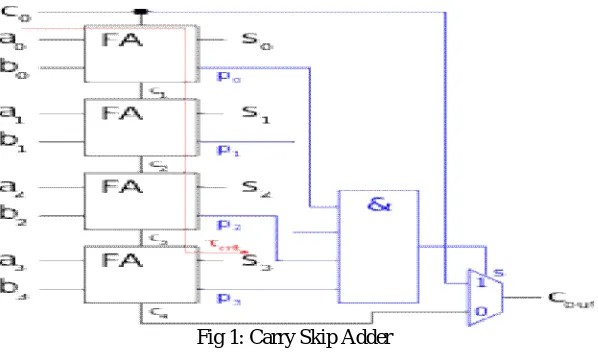
A CSKA consists of full adder gates and multiplexer logic this configuration strongly affects the speed. These full adder blocks are connected by 2:1 multiplexers. A below Figure (1) shows a normal carry skip adder.
Fig 1: Carry Skip Adder
Instead of the constant block size, we can use a variable block size to improve the performance of the CSKA. The number of bits can be further increased the propagation delay of the CSKA, An adder should be considered optimal if it is not possible to add bits without increasing the delay.
B. CONVENTIONAL CARRY SKIP ADDER:
The Conventional carry skip adder (Conv-CSKA) structure consist of the ripple carry adder blocks (RCA) and multiplexers. Each Ripple carry adder to produce a carry and it will be fed into the multiplexer block for skip logic. At each stage inputs of the multiplexer are the carry input of the stage and the carry output of its RCA stage. Consider this is an N-bit RCA so it contains N cascaded Full adders (FAs), which lead the worst propagation delay. This propagation delay belongs to the two inputs X and Y. The below expression shows the dependencies between propagation delay and inputs for N-bit RCA,
= ⊕ = 1 For i =1,…, N
Where Pi is the propagation delay, Xi and Yi are inputs or two numbers to be added. Fig.2 shows the structure of Conventional carry skip adder. This CSKA can be implemented using two methods one is fixed size stage (FSS) and variable size stage (VSS). These two methods are discussed in detail in the following section.
i) FSS-CSKA:
ISSN(Online): 2320-9801 ISSN (Print) : 2320-9798
I
nternational
J
ournal of
I
nnovative
R
esearch in
C
omputer
and
C
ommunication
E
ngineering
(An ISO 3297: 2007 Certified Organization)
Vol. 4, Issue 10, October 2016
stage (M × TCARRY). b) The path of the intermediate multiplexer ((Q-1) × TMUX), Where Q is an integer (Q=N/M). c)
The path of the full adder chain in the last stage (M-1) × TCARRY+ TSUM. Td = [M × TCARRY] +
[(
(N/M)-1) × TMUX]
+ [(M-1) × TCARRY+TSUM] (1)
The optimum value of M based on (1) is calculated and propagation delay may be (0.5Nα)1/2.α is equal to TMUX/TCARRY.
ii) VSS-CSKA:
In previous case block size is fixed but in this type variable block size is used to improve the speed of the CSKA. By lowering the delays of the first and last blocks of ripple carry adder paths improve the speed of the operation.
Fig.2.Conventional carry skip adder (Conv-CSKA)
The speed can be improved by lowering the delays of the first and third terms in (1).In conventional CSKA uses a multiplexer for skip logic. This variable size stage allows the other type of skip logic. So the equation for critical path written in more general form by replacing TMUX by TSKIP. The below equation reveals that large portion of delay
due to skip logics,
Topt = TCARRY + (2√N/α -1) TSKIP +TSUM (2)
C. HIGH-SPEED ENERGY EFFICIENT CARRY SKIP ADDER (CI-CSKA):
The above sections clearly present that delay mainly depends on the skip logic. Reducing the delay of multiplexer skip logic may reduce the propagation delay of Conv-CSKA. This structure is based on the concatenation and incrementation methods. This type is denoted by CI-CSKA. In this, the multiplexer skip logic can be replaced by And-Or-Invert (or) Or-And-Invert compound gates. These AOI/OAI compound gates consist of fewer transistors. The power consumption is less in this skip logic when compared to normal multiplexer logic [14]. In this structure, carry propagates through the skip logics and it produces complemented output. The structure has a lower propagation delay with a smaller area. The inverting gates of AOI and OAI are available in standard libraries; this is the reason of using this logic. In this way, increasing power consumption and delay is eliminated. The first skip logic uses the AOI logic then the next skip logic should use the OAI logic. In Conv-CSKA structure, the skipping structure increases the delay in the critical path.
In the Conv-CSKA, the multiplexer logic is not able to bypass the zero carry input until the zero carry input propagates from the RCA block. By using the concatenation approach this problem can be solved. The area and delay of this structure are mainly depending on the AOI/OAI compound gates. Static AOI and OAI compound gates use 6 transistors when the static 2:1 multiplexer uses 12 transistors. It’s clearly shown that number of transistors get reduced in modified skip logic so that the area and delay are reduced [14], [15].
ISSN(Online): 2320-9801 ISSN (Print) : 2320-9798
I
nternational
J
ournal of
I
nnovative
R
esearch in
C
omputer
and
C
ommunication
E
ngineering
(An ISO 3297: 2007 Certified Organization)
Vol. 4, Issue 10, October 2016
In FSS implementation (FSS-CI-CSKA), there are Q=N/M stages with the size of M. In VSS implementation (VSS-CI-CSKA), the size of the stages, which are M1 to MQ can be calculated using some methods.
Fig.3 shows the structure of CI-CSKA. In this structure, skip logic uses AOI and OAI compound gates.
Fig.3.modified structure (CI-CSKA)
In addition to this, an incrementation block is used. A and B are the inputs to the RCA blocks. In the first stage, zero carry and inputs are applied to the first RCA block. The carry output of the RCA fed into the AOI/OAI block. Final OAI gate produce carry output. The sum output is passed through the incrementation block to produce the addition output.
III. PROPOSED WORK
As mentioned in above section the speed of the normal carry skip adder improved by using incrementation and concatenation methods. The proposed work is also using these methods. Reducing the skip logic delay may reduce the overall propagation delay. The proposed system introduces the parallel prefix network to reduce the delay in variable latency CSKA.
In prior work Brent-Kung adder is used for the parallel prefix network. In addition to this several parallel prefix, adders are there, Kogge-Stone adder, Han-Carlson adder and Lynch-Swartzlander spanning tree adder. In the proposed system, we use the Kogge-Stone adder. It is a parallel prefix form carry look-ahead adder. It is the fastest adder when compared to Brent-Kung adder. For this reason, we choose this adder for proposed work.
For the proposed work parallel prefix network is included in between the stages of RCA as shown in Fig.3. This parallel prefix network combined with processing units is referred to as nucleus stage. The modified CSKA structure with parallel prefix network is shown in Fig.4. In this structure consist of two processing networks and parallel prefix adder network. The processing networks are used for different purposes. First one is used for pre-processing step and the second one is used for post-processing step. An input from the second RCA block is given to the parallel prefix network and the output of this network is fed to the third RCA network. This is a main modification in the proposed system.
The critical path from the first stage of RCA to last stage of RCA is termed as Long latency path (LLP). The path from the first stage of RCA to post processing network is termed as Short latency path 1 (SLP1) and the path from preprocessing unit to the last stage of RCA is termed as Short latency path 2 (SLP2).These two paths are considered for a calculation of critical path in the overall structure.
ISSN(Online): 2320-9801 ISSN (Print) : 2320-9798
I
nternational
J
ournal of
I
nnovative
R
esearch in
C
omputer
and
C
ommunication
E
ngineering
(An ISO 3297: 2007 Certified Organization)
Vol. 4, Issue 10, October 2016
Fig.4.modified CSKA with parallel prefix adder
The carries are generated vertically and these output bits are XOR’d with the initial propagate bits after the input to produce the sum output. This is a more efficient adder especially the power consumption of this adder is significantly low when compared to other adders. As shown in below adder the carry input is given into first vertical stage, this first stage performs the XOR’d operation. A carry may be considered as 0 or 1.In this example, it is taken as 0.
The functioning of Kogge-Stone adder (KSA) is divided into three parts. These are1) Pre-processing, 2) Carry look ahead network, 3) Post processing. In a Pre-processing step, propagate and generate signal bits are generated for the pair input bits A and B.
Pi = Ai XOR Bi
Gi = Ai AND Bi
A carry look ahead block differentiates Kogge-Stone adder from others. This is the main difference to make this adder has more high performance. This step produce carries for each bit and it uses group propagate and generates given by the equations,
Pi:j = Pi:k+1 AND Pk:j
Gi:j = Gi:k+1 OR (Pi:k+1 AND Gk:j)
Post processing is the final step of this KSA and it is also common to all adders of this carry look ahead families. Sum bits are generated by using below equation,
Si=Pi XOR Ci-1
Fig.5. Example of 8-bit Kogge-Stone adder structure
ISSN(Online): 2320-9801 ISSN (Print) : 2320-9798
I
nternational
J
ournal of
I
nnovative
R
esearch in
C
omputer
and
C
ommunication
E
ngineering
(An ISO 3297: 2007 Certified Organization)
Vol. 4, Issue 10, October 2016
IV. RESULTS AND DISCUSSION
In this section, the simulation outputs of the proposed carry skip adder are explained. The carry skip adder can be simulated using Modelsim 6.4a and synthesized using ISE design suite. The below Fig.6 shows the output of modified high speed carry skip adder. The output of this high-speed CSKA also gives same output of ordinary adders. But by using this modified high-speed carry skip produce the output with minimum delay time. In the proposed system, we explain the Example of 4-bit Kogge-Stone adder. This output taken for overall output of modified high speed carry skip adder. Here the values are given only for A and B. The carry may be either zero or one. The design functionality has been verified using Xilinx ISE design suite 14.5.Energy-delay product of Kogge-stone adder is small so that the energy of the modified high-speed adder is less when compared to the Conv-CSKA.
Fig.6.Simulation output of Modified CSKA using Modelsim 6.4a.
The technology schematic shows the detailed architecture of modified high speed carry skip adder. This can be viewed by using Xilinx ISE suite. The technology schematic of this modified carry skip adder is shown in below Fig.7.This is for detailed architecture; here it shows all the connections and parameters in the structures. These two schematics are viewed by the use of ISE suite. The power (energy) and time are taken from design summary produced by the ISE.
ISSN(Online): 2320-9801 ISSN (Print) : 2320-9798
I
nternational
J
ournal of
I
nnovative
R
esearch in
C
omputer
and
C
ommunication
E
ngineering
(An ISO 3297: 2007 Certified Organization)
Vol. 4, Issue 10, October 2016
Fig.8 RTL schematic
The RTL schematic is a Register Transfer Level schematic, which shows the transistor level design of the circuit. The below Fig.8 shows the RTL schematic of a modified high speed carry skip adder. Here there are three blocks one is a Kogge-stone adder block, the second one is an incrementation block and an interior block is an And-Or-Invert and Or-And-And-Or-Invert skip logic block.
V. CONCLUSION
In this paper, a structure called modified high speed carry skip adder (CSKA) was proposed. The main advantage of this paper is its ability to add two inputs with minimum delay time. This reduction in delay time can be achieved by using a parallel prefix adder network (PPA). This parallel prefix adder is inserted in the middle stages of RCA chain. The Kogge-Stone adder is used for this parallel prefix network. In addition to this, the power consumption of this structure is reduced by using AND-Or-Invert and Or-And-Invert gates for skip logics. An incrementation scheme increases the speed of the structure. These two modifications make this modified carry skip adder more efficient.
R
EFERENCES1. Milad Bahadori, Mehdi Kamal, Ali Afzali-Kusha, Senior Member, IEEE, and Massoud Pedram, Fellow, IEEE “high-speed and energy efficient carry skip adder operating under a wide range of supply voltage levels”1063-8210 ©
2. R. Zlatanovici, S.Kao, and B.Nikolic, “Energy–delay optimization of 64-bit carry-look-ahead adders with a 240 ps 90 nm CMOS design example,” IEEE J. Solid-State Circuits, vol. 44, no. 2, pp. 569–583,Feb.2009.
3. S. K. Mathew, M. A. Anders, B. Bloechel, T. Nguyen, R. K. Krishnamurthy, and S. Borkar, “A 4-GHz 300-mW 64-bit integer execution ALU with dual supply voltages in 90-nm CMOS,”IEEE J. Solid-State Circuits, vol. 40, no. 1, pp. 44–51, Jan. 2005.
4. V. G. Oklobdzija, B. R. Zeydel, H. Q. Dao, S. Mathew, and R. Krishnamurthy, “Comparison of high-performance VLSI adders in the energy-delay space,” IEEE Trans. Very Large Scale Integr. (VLSI)Syst., vol. 13, no. 6, pp. 754–758, Jun. 2005.
5. B. Ramkumar and H. M. Kittur, “Low-power and area efficient carry select adder,” IEEE Trans. Very Large Scale Integr. (VLSI) Syst., vol. 20, no.2, pp.371–375, Feb.2012.
6. M. Vratonjic, B. R. Zeydel, and V. G. Oklobdzija, “Low- and ultra low-power arithmetic units: Design and comparison,” in Proc. IEEEInt. Conf. Comput. Design, VLSI Comput. Process. (ICCD), Oct.2005, pp.249–252.
7. C. Nagendra, M. J. Irwin, and R. M. Owens, “Area-time-power tradeoffs in parallel adders,” IEEE Trans. Circuits Syst. II, Analog Digit. Signal Process, vol. 43, no. 10, pp. 689–702, Oct. 1996.
8. Y. He and C.-H. Chang, “A power-delay efficient hybrid carry look ahead/carry-select based redundant binary to two’s complement converter,”
IEEE Trans. Circuits Syst. I, Reg. Papers, vol.55, no.1, pp.336–346, Feb.2008.
9. C.-H. Chang, J. Gu, and M. Zhang, “A review of 0.18 μm full adder performances for tree structured arithmetic circuits,” IEEE Trans. Very Large Scale Integr. (VLSI) Syst., vol. 13, no. 6, pp. 686–695, Jun. 2005.
ISSN(Online): 2320-9801 ISSN (Print) : 2320-9798
I
nternational
J
ournal of
I
nnovative
R
esearch in
C
omputer
and
C
ommunication
E
ngineering
(An ISO 3297: 2007 Certified Organization)
Vol. 4, Issue 10, October 2016
11. M. Lehman and N. Burla, “Skip techniques for high-speed carry propagation in binary arithmetic units,” IRE Trans. Electron. Comput, vol. EC-10, no. 4, pp. 691–698, Dec. 1961.
12. “Design and Performance Analysis of Various Adders using Verilog” Maroju SaiKumar, Dr. P. Samundiswary, IJCSMC, Vol. 2, Issue. 9, September 2013.
13. Koren, Computer Arithmetic Algorithms, 2nd ed. Natick MA, USA: A K Peters, Ltd. , 2002.
14. J. M. Rabaey, A. Chandrakasa, and B. Nikolic, Digital Integrated Circuits: A Design Perspective, 2nd ed. Englewood Cliffs, NJ, USA: Prentice-Hall, 2003.
15. Nan Gate 45nm Open Cell Library. [Online]. Available: http://www.nangate.com/, accessed Dec. 2010.
16. Y.-S. Su, D.-C. Wang, S.-C. Chang, and M. Marek-Sadowska, “Performance optimization using variable-latency design style,” IEEE Trans. Very Large Scale Integr. (VLSI) Syst., vol. 19, no. 10, pp.1874–1883, Oct. 2011.
17. Y. Chen, H. Li, J. Li, and C. - K. Koh, “Variable-latency adder (VL-adder): New arithmetic circuit design practice to overcome NBTI,” in Proc. ACM/IEEE Int. Symp. Low Power Electron. Design (ISLPED), Aug. 2007, pp. 195–200.
BIOGRAPHY
R.Ezhilarasi is an M.E scholar in VLSI design in the Electronics and Communication Department, Karpaga Vinayaga College of Engineering and Technology, Affiliated to Anna University. She received B.E degree in 2015 from Anna University, Chennai, Tamil Nadu, and India. Her research interests are Modern VLSI and System on Chip.