ABSTRACT
TEDESCO, JOSEPH LEO. Electrical Characterization of Transition Metal Silicide Nanostructures Using Variable Temperature Scanning Probe Microscopy. (Under the direction of Robert J. Nemanich.)
Cobalt disilicide (CoSi2) islands have been formed on Si(111) and Si(100) through UHV deposition and annealing. Current-voltage (I-V) and temperature-dependent current-voltage (I-V-T) curves have been measured on the islands using conducting atomic force microscopy (c-AFM) with a doped diamond like carbon cantilever. Thermionic emission theory has been applied to the curves and the Schottky barrier heights, ΦB, and ideality factors, n, for each island have been calculated. Barrier heights and ideality factors are evaluated as functions of temperature, island area, and each other. While all islands were prepared in UHV conditions, one set was removed from UHV and measurements were performed in ambient conditions while the other set remained in UHV. The islands measured in ambient conditions were known as “air-exposed samples” due to the fact that the surface was assumed to be passivated upon exposure to atmospheric conditions. The islands measured in UHV were known as “clean samples” because the surface was not passivated. Air-exposed samples were CoSi2 islands on Si(111) and exhibited a negative linear
height as a function of decreasing island area was detected in all samples. This trend is attributed to increased hole injection and generation-recombination in the smaller islands, but it may also be due to effects caused by increased spreading resistance as the island size decreases. Non-linearity in activation energy plots, as well as correlations between
decreasing barrier height and decreasing island area-to-island periphery ratio, are attributed to generation-recombination. These measurements indicate that the Schottky barrier height decreases and ideality factor increases with decreasing temperature, even if there is no direct linear correlation between ΦB and n. These temperature-dependent relationships are
attributed primarily to hole injection and generation-recombination, with barrier height inhomogeneity as a minor effect.
Titanium silicide (TiSi2) islands have been formed by UHV deposition of titanium on atomically flat Si(100) and Si(111). Scanning tunneling microscopy (STM), scanning
Electrical Characterization of Transition Metal Silicide
Nanostructures Using Variable Temperature
Scanning Probe Microscopy
by
Joseph Leo Tedesco
A dissertation submitted to the Graduate Faculty of North Carolina State University
in partial fulfillment of the requirements for the Degree of Doctor of Philosophy
Physics
Raleigh, North Carolina 2007
APPROVED BY:
DEDICATION
BIOGRAPHY
Joseph Leo Tedesco was born on June 20, 1979 to Patrick and Cecile Tedesco of Virginia Beach, VA. He has one sister, Marie, who was born just over three years later. His early childhood was spent, as most young boys’ early lives should be, with playing outside and going to school. He was a good student, and despite a penchant in the early grades for not finishing his work, he enjoyed learning and was naturally curious. He played soccer and baseball, but he knew that his future never lay in the athletic world.
He developed an interest in math and science early on, and his career aspirations extended from them, moving from writer (still an interest), to architect, to architectural engineer. In the eighth grade, he developed an interest in astrophysics and that was that. He graduated from Tallwood High School in Virginia Beach, VA in June of 1997, and that Fall began his studies at the University of Virginia with the intention of studying astrophysics. He quickly reached the conclusion that while he enjoyed astrophysics and found it interesting, he did not want to make it a career. Over the next few years, he happened upon condensed matter physics, and decided that he liked the field enough that he could spend his life in the field. With that in mind, he applied to several graduate schools, all of which had strong research programs in condensed matter, and was accepted to North Carolina State University. After graduating from the University of Virginia, he moved to Raleigh, and joined the
Surface Science Lab on June 25, 2001.
During his time at the University of Virginia, not only did he happen upon the field of condensed matter physics, but he also found the woman who would become his wife,
finally began dating and became inseparable. They were engaged in April of 2001 and married in June of 2004.
In the meantime, he had been working for Dr. Nemanich as a member of the Surface Science Lab and taking classes. He passed the Ph.D. Qualifying Examination in April and May of 2003. This was when the Qualifier consisted on four hour tests in the both morning and afternoon, on Monday, Wednesday, and Friday.
ACKNOWLEDGMENTS
Throughout this entire process, I have had the complete and total support of my wonderful wife, Stephanie. Her love has made all the difference in things being bearable or not. And her occasional motivational foot in the rear helped me to get a move on and get into the lab. It’s not that I’m not motivated, but sometimes it takes a little bit of time for me to get going. Her pushing me was an immense help. Additionally, her tactic of allowing me to “not exist” when it came to housework and cooking and things of that sort so that I could finish my defense and dissertation was invaluable. I thank her for everything she did.
My parents, Patrick and Cecile, and my wife’s parents, Orville and Barbara Mullins, were also constant sources of support. They never stopped believing in me, and they always encouraged me. They never grew tired of hearing about what I was doing. I thank them for that and for helping me to feel that I was working toward something. I also want to thank my sister, Marie, and my brother-in-law, Jeff, for always making it sound like what I was doing was so complicated and impressive.
I also want to thank my little dog, Baby Pup, for always being there to provide constant love and the need to go for a walk. It’s hard to be unhappy when you get home and your dog runs up to you and jumps up and down. She also helped keep me grounded by wanting to go for those walks, regardless of what was going on. She provided love and joy and I want to thank her for that.
broke. I know that you learn a lot about something by repairing it, but you can also learn a lot without breaking things. So, I thank him for putting up with the slow periods of research that seemed to dominate the early part of my career.
I would also like to thank Dr. Jack Rowe, who stepped in as my day-to-day advisor when Dr. Nemanich left NC State to become the chair of the Physics Department at Arizona State University. He had different ideas than Dr. Nemanich, and different experiences in the field, and so he provided a different outlook on my research. I thank him for that.
I also thank the other members of my committee, Dr. Thomas Pearl and Dr. Carlton Osburn. They helped out and provided insight into my research. Their advice helped to steer me in the directions I needed to go.
The Nemanich group has always been like a small army, and as such its members are numerous. Nevertheless, there are a few who I feel deserve special thanks. I would like to thank Dr. Jaehwan Oh, for introducing me to STM and for teaching me how to operate the Small System. I would also like to thank Dr. Matt Zeman, for always being willing to talk about research and for putting up with the entropy that surrounded my desk when we shared an office. I would also like to thank Dr. Brian Rodriguez for guidance pertaining to AFM and research in general. A thank you goes to Dr. Anderson Sunda-Meya for his advice during the heteroepitaxy meetings. A quick thank you also goes to Dr. Jamie Perkins for being willing to talk about just about physics or research, which helped to pass the time, particularly during long experiments.
Hartlieb, Tom Blair, Andrew DeAndrade, Jacquie Hanson, Jon Waldrep, Brendan Shields, Mike Shields, Franz Koeck, Dr. Yunyu Wang, Eugene Bryan, Dr. Jacob Garguilo, Dr. Ted Cook, Dr. Charlie Fulton, Dr. Jaesob Lee, Erica Robertson, Dr. Brian Coppa, Dr .Will MeCouch, Dr. Yingjie Tang, Jiyoung Chung, Xinhua "Wendy" Kong, Liegh Winfrey, Dr. James Burnette, Jennifer Walters-Huening, Luke Bilbro, Dr. Joshua Smith, Xin Li, Dong Wu, Stefan Habicht, Marcel Himmerlich, Carsten, Nina Malchus, Andreas Sandin, and Zhengang Wang.
When I first arrived at NC State in 2001, someone else in the department from outside the Nemanich group (I don’t remember who, it may have even been a faculty member) told me that the Nemanich group was like a clique. It’s not hard to see how one would come to that conclusion. During my graduate career, the Nemanich group always had at least a dozen members (and usually more) and we spent much of our time around each other doing
research, and not out around other members of the graduate school. This wasn’t a universal truth, but I found that it was pretty close to one. Therefore, the vast majority of friends I gained at NC State came from within the Nemanich group. However, there are a few friends that came from outside the group. I count Veda Bharath, Nancy Santagata, Matt Walker, Sharon Kiesel, Matt Lewis, Dave Baker, Brian Davis, Franklin DuBose, Bev Clark, and Dr. Simon Lappi among my friends from outside the group. I’m sure that I have forgotten several other people that I consider friends. Please don’t take it personally. I thank each one of you.
weren’t around for whatever reason. I would also like to thank Jenny Allen for helping coordinate matters with the graduate department and make sure I had all my ducks in a row. She was also one of the nicest people.
I would also like to give an extremely grateful thank you to Tim Harvell, Frank, Mike, and the other members of the PAMS Machine Shop since 2001. They were an immense help to my research and didn’t complain when I came in with a part that had to be done within two days or when I came in with metric dimensions on my drawings. They were master machinists and took care of everything I needed fabricated or repaired.
I would also like to thank the service engineers from Omicron Nanotechnology. Dave Wynia was invaluable installing the Multiprobe P and teaching me how to use it. He was also available to answer questions and offer assistance. Matt Roberts was also an invaluable aid in offering support and answering questions. Alex Skripnik was also helpful in answering questions and solving problems.
I’m sure that there are many others who I should be thanking who I have left of this list. Believe me when I say that it is not an intentional insult. So, to all of you, thank you.
And last, but by no means least, I would like to thank God, who managed to find time to watch over and guide me, despite having a very busy schedule of taking care of the
TABLE OF CONTENTS
List of Figures ... xiii
List of Tables ... xix
Chapter 1: Introduction ... 1
1.1. Motivation ... 1
1.2. Scope of the Dissertation ... 3
References ... 5
Chapter 2: Theoretical Background ... 6
2.1. Introduction ... 6
2.2. Scanning Probe Microscopy ... 6
2.2.1. Scanning Tunneling Microscopy ... 7
2.2.1.1. Tunneling Tip... 7
2.2.1.2. Sample... 12
2.2.1.3. Other Considerations ... 13
2.2.2. Atomic Force Microscopy ... 13
2.2.2.1. Contact Mode Atomic Force Microscopy ... 14
2.2.2.2. Conducting Atomic Force Microscopy ... 16
2.3. Additional Surface Analysis Techniques ... 18
2.3.1. Scanning Tunneling Spectroscopy ... 18
2.3.1.1. Current Imaging Tunneling Spectroscopy (CITS) ... 21
2.3.2. Auger Electron Spectroscopy ... 22
2.3.3. Low Energy Electron Diffraction ... 23
2.4. Summary of Relevant Transition Metal Silicides ... 25
2.4.1. Cobalt ... 25
2.4.1.1. Formation of CoSi2... 25
2.4.1.2. Interfacial Coordination ... 26
2.4.2. Titanium ... 27
2.4.2.1. Formation of TiSi2 ... 28
2.5. Metal-Semiconductor Interfaces ... 28
2.5.1. Basic Characteristics of Metal and Semiconductor Surfaces ... 29
2.5.2. Schottky Barrier ... 30
2.5.2.1. Models of Schottky Barrier Formation ... 31
2.5.2.1.1. Schottky-Mott Model ... 31
2.5.2.1.2. Metal-Induced Gap States (MIGS) Model ... 32
2.5.2.1.3. Schottky Barrier Inhomogeneity Model ... 33
2.5.3. Current Transport across the Schottky Barrier ... 34
2.5.3.1. Thermionic Emission ... 35
2.5.3.2. Thermionic Field Emission (TFE) ... 37
2.5.3.3. Field Emission ... 38
2.5.3.4. Recombination in the Depletion Region ... 38
2.6. Single Electron Tunneling (SET)... 40
2.6.1 Coulomb Blockade... 45
2.6.2. Coulomb Staircase ... 46
References ... 48
Figures... 54
Chapter 3: Experimental Facilities and Procedures ... 65
3.1. Introduction ... 65
3.2. UHV Systems... 65
3.2.1. Multiprobe P Surface Science System ... 66
3.2.2. Small System ... 75
3.2.3. Integrated Surface Analysis and Growth System (ISAGS) ... 79
3.3. Ambient Systems ... 81
3.3.1. Atomic Force Microscopy (AFM) Systems ... 82
3.3.1.1. Autoprobe CP-Research... 82
3.3.1.2. Autoprobe M5 ... 84
3.3.2. Testing Station ... 85
3.4. Experimental Procedures ... 87
3.4.1. Sample Preparation Procedures ... 87
3.4.1.1. Substrates for room temperature c-AFM study ... 87
3.4.1.2. Substrates for variable temperature c-AFM study ... 89
3.4.1.3. Substrates for SET study ... 92
3.4.2. STM/AFM Procedures ... 93
3.4.2.1. Room temperature c-AFM study ... 93
3.4.2.2. Variable temperature c-AFM study ... 94
3.4.2.3. SET study ... 95
References ... 97
Figures... 100
Chapter 4: Current-Voltage Measurements of Cobalt Disilicide Islands using Conducting Atomic Force Microscopy ... 114
4.1 Abstract ... 114
4.2. Introduction ... 115
4.3. Experimental ... 116
4.3.1. Air-exposed surfaces ... 117
4.3.2. Clean surfaces ... 119
4.4. Results ... 122
4.4.1. CoSi2/Si(111) ... 122
4.4.1.1 Electrical Characteristics of Air-exposed Surface Islands ... 122
4.4.1.2. Interfacial Structure of Air-exposed Surface Islands ... 123
4.4.1.3. Electrical Characteristics of CS111 Islands ... 124
4.4.2. CoSi2/Si(100) ... 125
4.5. Discussion ... 126
4.5.1. Common Phenomena ... 126
4.5.3. Air-exposed Surface Islands ... 130
4.5.3.1. Island Shape and Interfacial Structure ... 130
4.5.3.2. Schottky Barrier Height Relationships ... 131
4.5.4. Clean Surface Samples ... 132
4.5.4.1. Room Temperature Barrier Height Relationships for CS111 ... 132
4.5.4.2. Room Temperature Barrier Height Relationships for CS100 ... 132
4.5.4.3. Fermi Level Pinning ... 133
4.5.4.4. Temperature Dependent Analysis ... 134
4.5.4.5. Interfacial coordination ... 135
4.6. Conclusion ... 136
References ... 138
Figures... 142
Chapter 5: Variable Temperature Scanning Tunneling Microscopy and Spectroscopy of Titanium Silicide on Si(100) and Si(111) ... 159
5.1 Abstract ... 159
5.2. Introduction ... 160
5.3. Experimental ... 163
5.4. Results ... 166
5.4.1. Tunneling spectra of TiSi2 islands and confirmation of SET ... 166
5.4.2. Coulomb staircase at room temperature ... 167
5.5. Discussion ... 168
5.5.1. Analysis via the orthodox model ... 168
5.5.2. Discrepancies with predictions of the orthodox model ... 170
5.5.3. Absence of SET ... 172
5.6. Conclusion ... 177
References ... 178
Figures... 182
Chapter 6: Summary ... 188
6.1. Introduction ... 188
6.2. Conclusions of work concerning CoSi2 ... 189
6.3. Conclusions of work concerning TiSi2... 192
References ... 195
Tables ... 197
Chapter 7: Future Research ... 198
7.1. Introduction ... 198
7.2. Schottky Barrier Height Measurements ... 198
7.2.1. Interfacial Structure of a Nanocontact and Its Ideality Factor ... 198
7.2.2. Impact of Surface States ... 199
7.3. Single Electron Tunneling Measurements ... 200
7.3.1. Effect of Doping Concentration on SET ... 200
7.3.2. Interfacial Effects on SET ... 201
7.4. Linear Transport Properties of Nanowires ... 203
7.4.1. Conductance Quantization ... 204
7.4.2. Size Dependence of Nanowire Electrical Characteristics ... 205
7.5. Conclusion ... 206
References ... 208
LIST OF FIGURES
Figure 2.1: Simplified schematic view of an STM [6]. ... 54 Figure 2.2: STM error signal image of a Si(111):7×7 surface that exhibits step bunching. Scan size: 30 nm × 30 nm. Note that there is evidence of atomic resolution in the individual steps within the step bunch [21]. ... 55 Figure 2.3: (a) Basic operational principle of the AFM [26]. (b) Basic schematic of c-AFM measurements presented in Chapter 4... 56 Figure 2.4: STS data recorded on a TiSi2 nanoisland grown on Si(111). Note that small changes in the structure of the I-V curve can lead to pronounced peaks in the V
dV dI − ⎟ ⎠ ⎞ ⎜ ⎝ ⎛
of the DBTJ. (c) Band diagram of the DBTJ. Note that the example band diagram shows features an n-type semiconductor, however, the theory would be successful with a p-type semiconductor, as well. ... 63
Figure 2.11: Simplified diagrams of I-V and V dV dI − ⎟ ⎠ ⎞ ⎜ ⎝
⎛ curves that demonstrate SET
signatures. (a) Simplified (i) I-V curve and (ii) V dV dI − ⎟ ⎠ ⎞ ⎜ ⎝
⎛ curve for the Coulomb blockade.
(b) Simplified (i) I-V curve and (ii) V dV dI − ⎟ ⎠ ⎞ ⎜ ⎝
⎛ curve for the Coulomb staircase. ... 64
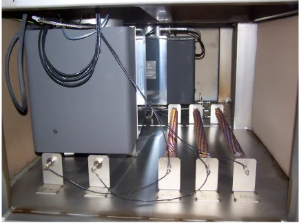
Figure 3.1: Multiprobe P Surface Science System. Labeled arrows identify the three main UHV chambers, the preparation and analysis chambers, as well as the chamber housing the microscope. The unlabeled arrows indicate the magnetic probes used to transfer samples and tip carriers between chambers. ... 100 Figure 3.2: Space underneath the Multiprobe P containing the ion pumps. The ion pump in the foreground is for the analysis chamber while the far ion pump is for the preparation chamber. To the right of the analysis chamber ion pump and each ion pump are heating coils used during bakeouts... 101 Figure 3.3: Multiprobe P bakeout cover in place. Note that the transfer arm is covered with its own custom insulated cover, indicated by an arrow, because it extends outside of the confines of the bakeout cover. A similar insulated cover is placed on the other transfer arm (with the magnetic probes removed), allowing the transfer arms to be baked with the rest of the chamber. ... 102 Figure 3.4: Crucibles used in the EFM 3T. (a) Custom-made molybdenum crucible used for the evaporation of cobalt. (b) Commercial crucible, manufactured by Focus, used for
evaporating gold. Note that the arrow indicates a small piece of molybdenum that is designed to prevent the ceramic liner from charging while the gold source is bombarded with electrons during evaporation. The component that is circled is the barrel connector used for mounting the crucible inside the EFM 3T. ... 103 Figure 3.5: The microscopy half of the analysis chamber. Note that the wobblestick is
Figure 3.6: Sample cartidges for use with the Multiprobe P Surface Science System. The tab used for maneuvering samples with the wobblestick is indicated on the stainless steel sample plate and is the same for all sample cartridges. Note that some ceramic top plates are
discolored due to extreme heat during annealing. a) Sample plate. There are two types of flat metal samples plates: molybdenum and stainless steel. b) Cooling sample cartridge. This type of sample cartridge has no electrical contacts in order to minimize thermal losses, but can only operate at either room temperature or ~25 K because samples cannot be counter-heated without electrical contacts. c) Resistive heating sample cartridge. This type of sample cartridge, despite its name, contains a PBN heater for radiatively heating samples. d) Direct current heating sample cartridge. e) Direct current heating sample cartridge with additional tantalum foil pieces for c-AFM studies. The tantalum pieces are typically separated by ~1 mm during use. f) Direct current heating sample cartridge with a silicon wafer piece
Figure 3.12: Configuration of the ISAGS in 2000 [24]. Note that double chambers are piggy-backed and transferring to the second chamber from the transfer line required transferring through the first chamber. ... 111 Figure 3.13: Current configuration of the ISAGS. Note that chambers with slashes (i.e. AES/LEED) are not piggy-backed, but have multiple functionalities. Also, the BCN
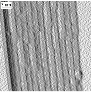
Microwave chamber is currently not present, but is included in the plans for the ISAGS. .. 112 Figure 3.14: a) STM image of Si(111):7×7 surface handled with stainless steel tweezers. Scan size: 125 nm. Tip bias: +1.0 V. Tunneling setpoint: 1.0 nA. b) STM image of Si(100):2×1 surface handled with ceramic tweezers. Scan size: 250 nm. Tip bias: +1.0 V. Tunneling setpoint: 1.0 nA. c) STM image of Si(100): 2×1 surface handled with stainless steel tweezers. Scan size: 200 nm. Tip bias: +1.5 V. Tunneling setpoint: 1.0 nA. The ordered lines of vacancies on the Si(100) surface have been attributed to nickel contamination from the stainless steel tweezers. ... 113 Figure 4.1: AFM image of CoSi2/Si(111) islands from Air-exposed sample. (a) AFM
topographical scan. Scan size: 3.0 μm. Note that triangular and non-triangular islands grow in the vicinity of each other, however, the majority of non-triangular islands appear to have irregular hexagonal shapes. (b) Error signal of the scan shown in (a). (c) AFM topographical scan. Scan size: 3.0 μm. Note that there are non-triangular islands that are not hexagonal in shape, such as the circled island. (d) Error signal of the scan shown in (c). ... 142 Figure 4.2: CoSi2/Si(111) islands from CS111. (a) AFM topographical scan. Scan size: 10.0 μm. (b) Error signal of the scan in (a). (c) AFM topographical scan of a close-in image of the lower right region of the scan in (a). Scan size: 3.0 μm. (d) Error signal of the scan in (c). 143 Figure 4.3: The relationship between Schottky barrier height, ΦB, and ideality factor, n, for CoSi2 islands on Air-exposed sample. The data points are divided between those islands that are triangular in shape (▲) and those that are non-triangular in shape (●). A thick line (▬) marks the value of ΦB reported in the literature for bulk CoSi2/n-Si(111) [53]. The two islands that are outliers are indicated with AFM error signal scans to indicate their
that darker colors in the topographical scans (and brighter colors in the error signals) indicate the surface is recessed into the substrate. ... 146 Figure 4.6: Ambient temperature Schottky barrier height and ideality factor for CoSi2 islands on CS111. As in Figure 4.3, the data points are divided between those islands that are
triangular in shape (▲) and those that are non-triangular in shape (●). ... 147 Figure 4.7: Ambient temperature areal relationships for CoSi2 islands on CS111. (a) ΦB as related to island area and (b) n as related to island area. The data points for both (a) and (b) are divided between those islands that are triangular in shape (▲) and those that are non-triangular in shape (●). ... 148 Figure 4.8: ΦB as a function of temperature for CoSi2 islands on CS111. (a) ΦB(T) for
triangular islands and (b) ΦB(T) for non-triangular islands. ... 149 Figure 4.9: Ideality factor as a function of temperature for CoSi2 islands for CS111. (a) n(T) for triangular islands and (b) n(T) for non-triangular islands. ... 150 Figure 4.10: Activation energy plot for CoSi2 islands on CS111. (a) Activation energy plot for triangular islands. (b) Activation energy plot for non-triangular islands. ... 151 Figure 4.11: CoSi2 islands on CS100. (a) AFM topographical scan of the islands. Scan size: 20.0 μm. Note that the islands are rectangular and the tapered appearance of some of the islands is an image processing artifact. (b) Error signal of the image shown in (a). (c) Detail of rectangular islands. Scan size: 3.0 μm. Note that these islands do not appear in (a). (d) Error signal of the image shown in (c)... 152 Figure 4.12: Room-temperature Schottky barrier height and ideality factor for CoSi2 islands on CS100. ... 153 Figure 4.13: Room temperature areal relationships for CoSi2 islands on CS100. (a) ΦB as related to island area and (b) n as related to island area. ... 154 Figure 4.14: Temperature dependent electrical characteristics of CoSi2 islands on CS100. (a) ΦB(T) measurements and (b) n(T) measurements. ... 155
Figure 5.1: a) Simplified drawing of DBTJ in these experiments. b) Diagram of the band structure associated with the DBTJ structure shown above. Note that this represents the band structure for the equilibrium case (V=0) when ND ~ 1017 cm-3. ... 182 Figure 5.2: TiSi2 islands grown on silicon surfaces. (a) STM image of TiSi2 islands on a Si(100) surface. Scan size: 150 nm. Tip bias: +1.0 V. Tunneling setpoint: 1.0 nA. (b) STM error signal image of TiSi2 islands shown in (a). (c) STM image of TiSi2 on a Si(111) surface. Scan size: 150 nm. Tip bias: +1.0 V. Tunneling setpoint: 1.0 nA. (d) STM error signal image of TiSi2 islands shown in (c). ... 183 Figure 5.3: Image and line scans of TiSi2 islands on Si(100). (a) STM image of TiSi2 islands on n-type Si(100):2×1. Scan size: 150 nm. Tip bias: +1.0 V. Tunneling setpoint: 1.0 nA. (b) Line scan of island labeled by numbers 1 – 3. (c) Line scan of island labeled by numbers 4 – 6. (d) Line scan of island labeled by numbers 7 – 9. ... 184
Figure 5.4: (a) I-V and V dV dI − ⎟ ⎠ ⎞ ⎜ ⎝
⎛ curves of the island labeled “2” in Figure 5.3(b). (b) I-V
and V
dV dI − ⎟ ⎠ ⎞ ⎜ ⎝
⎛ curves of the island labeled “5” in Figure 5.3(c). (c) I-V and V
dV dI − ⎟ ⎠ ⎞ ⎜ ⎝ ⎛
curves of the island labeled “8” in Figure 5.3(d). ... 185 Figure 5.5: Distribution of islands sizes for round islands grown on (a) Si(100) surfaces and (b) Si(111) surfaces. ... 186 Figure 5.6: (a) STM image of TiSi2 islands close together. Scan size: 40 nm. Tip bias: +1.0 V. Tunneling setpoint: 1.0 nA. The distance between islands 1 and 2 is ~2.5 nm while the distance between islands 2 and 3 is ~1.3 nm. (b) I-V and V
dV dI − ⎟ ⎠ ⎞ ⎜ ⎝
⎛ curves recorded from
LIST OF TABLES
Chapter 1:
Introduction
1.1. Motivation
In 1965, Gordon Moore of Fairchild Semiconductor made the bold prediction that the number of transistors that could be put on a microchip would double approximately every two years [1]. This exponential increase would lead to increases in processor speed and memory capacity, as well as decreases in overall device size. His prediction was born of his observations of the state of the semiconductor device industry to that point. Nevertheless, looking back over the years, his prediction has held up remarkably well. However, the trend that Moore predicted may be nearing an end.
The trend has been facilitated by ever-smaller transistors that allow for ever-faster processor designs. The basic structure and composition of these transistors has remained essentially the same. As a result, there are problems that may arise with the current
technology long before reaching the absolute physical limits imposed by quantum mechanics. [2]. Silicon-based integrated circuits are rapidly approaching operational limits because of issues with heat dissipation, power density requirements, and current leakage. In order to solve these problems, the semiconductor industry is moving in the direction of using
The International Technology Roadmap for Semiconductors (ITRS) has predicted that the current device structure will endure and that decreases in size and advances in speed will continue into the future [4]. Nevertheless, research is being performed to investigate the possibility of utilizing new device structures in order to take advantage of
previously-inaccessible physical phenomena. One such area of research into new device structures is research into single-electron devices [5-7].
Single electron devices will most likely utilize nanostructures as their base
components because nanostructures offer a variety of advantages, from their ability to self-assemble and be used in “bottom-up” device construction [8] to their novel electrical
properties. Self-assembly and nanostructure dynamics have been studied extensively [9-12], but in order to fully incorporate nanostructures into future device structures, the electrical characteristics must be studied further. In order to accurately study the characteristics of single nanostructures, a technique must be used that is capable of probing on a scale of several nanometers. This suggests that scanning probe microscopy will be an ideal technique.
transport processes occurring at the nanoscale CoSi2/Si interface. Furthermore, an investigation into variable temperature single electron tunneling (SET) from TiSi2
nanoislands will be presented. Together with the Schottky barrier height study, the variable temperature SET investigation will deepen the understanding of the electrical characteristics of these silicide nanostructures.
1.2. Scope of the Dissertation
This dissertation has been organized to follow a logical progression from beginning to end. An effort was made for this dissertation to build from an initial level, introduce the experimental studies, and draw conclusions from those studies.
As is the case for any experimental study, it is supported by the theoretical
information arrayed throughout the literature. Chapter 2 takes this vast array and condenses it into a more reasonable form. It contains the necessary background information to understand the experimental work presented later in the dissertation. The review includes the theory behind the relevant experimental techniques of scanning probe microscopy, spectroscopy, and surface analysis. It also presents an introduction to the theory behind the phenomena presented in later chapters. To that end, the review presents only the barest information regarding silicide nanostructure growth, instead focusing on electrical characterization.
Chapter 4 presents the investigation concerning variable temperature electrical characterization of CoSi2 islands. Schottky barrier heights and ideality factors are presented for CoSi2 islands grown via self-assembly on Si(111) and Si(100) substrates. The barrier heights and ideality factors were calculated from I-V curves measured at room temperatures and below. The data gathered from these islands is presented, and the temperature
dependence allows for a thorough examination of the current transport phenomena occurring in the CoSi2 islands.
Chapter 5 presents the investigation of SET in TiSi2 nanoislands grown on Si(111) and Si(100) substrates. The study presented in Chapter 5 differs from previous studies of SET in TiSi2 nanoislands because it contains a variable temperature component, whereas previous investigations of SET in TiSi2 nanoislands were only performed at room
temperature [13-14]. I-V and V dV
dI −
⎟ ⎠ ⎞ ⎜ ⎝
⎛ curves are presented, along with the analysis of
them that confirms the presence of SET. SET was not observed as often as expected, and Chapter 5 also contains an analysis of the reasons for this lack of observed SET.
References
[1] G.E. Moore, Electronics 38 (1965). [2] S. Lloyd, Nature 406 1047 (2000).
[3] R.K. Ashok, private communication (2007).
[4] Semiconductor Industry Association, International Technology Roadmap for Semiconductors at http://public.itrs.net (International SEMATECH, Austin, TX, 2007). [5] H. Ahmed and K. Nakazato, Microelectron. Eng. 32 297 (1996).
[6] S. Altmeyer, K. Hofmann, A. Hamidi, S. Hu, B. Spangenberg, and H. Kurz, Vacuum 52 295 (1998).
[7] K.K. Likharev, P. IEEE 87 606 (1999). [8] C.M. Lieber, MRS Bull. 28 406 (2003).
[9] M. Zinke-Allmang, L.C. Feldman, and M.H. Grabow, Surf. Sci. Rep. 16 377 (1992). [10] W.-C. Yang, M.C. Zeman, H. Ade, and R.J. Nemanich, Phys. Rev. Lett. 90 136102 (2003).
[11] M.C. Zeman, Ph.D. dissertation, North Carolina State University, Raleigh, NC (2007). [12] A. Sunda-Meya, Ph.D. dissertation, North Carolina State University, Raleigh, NC (2007).
[13] J. Oh, V. Meunier, H. Ham, and R.J. Nemanich, J. Appl. Phys. 92 3332 (2002).
Chapter 2:
Theoretical Background
2.1. Introduction
Experimental physics does not exist in a vacuum. While physical phenomena are often discovered experimentally before the theories that explain them are developed,
experiment and theory are nevertheless intimately intertwined. Well-conceived experiments tend to have a rigorous theoretical underpinning. The studies undertaken in this dissertation are no different. The following sections of this chapter contain the theoretical background necessary to interpret and understand the experimental results remainder of this dissertation.
2.2. Scanning Probe Microscopy
surface of interest, to collect data with a spatial resolution beyond the diffraction limit. It is this combination of raster scanning and utilizing a probe-sample interaction in the near-field regime, which lies at the center of scanning probe microscopy.
Scanning probe microscopy is used in many fields of study, but it is the electrical characterization of nanostructures that is the focus of this dissertation. In this dissertation, scanning tunneling microscopy (STM), as well as atomic force microscopy (AFM) and its derivative technique, conducting atomic force microscopy (c-AFM), are used to probe the electrical properties of transition metal silicide nanostructures.
2.2.1. Scanning Tunneling Microscopy
First invented in 1981 by Gerd Binnig and Heinrich Rohrer of IBM Zurich [2-5], the scanning tunneling microscope (STM) relies on quantum mechanical tunneling of electrons to study the material in question, with the potential to image with atomic scale resolution. The STM utilizes a sharpened metal tip positioned several Å above the sample under inspection. The mechanism used to probe the sample is quantum mechanical tunneling. The only true requirement is that the tip and the sample both be made of conductive material, because a tunneling current must be established between them when they are brought close together. A simple schematic of an STM [6] is shown in Figure 2.1. Several books and numerous review articles have been published related to STM [7-11].
2.2.1.1. Tunneling Tip
reason transition metals may be superior choices for use as STM tips due to the fact that their d-band electron orbitals are more pointed than the s-, p-, or f-band orbitals [9,12]. In addition to the electrical characteristics of the metal, considerations must be made as to the
environment that the tip will encounter, whether that environment will be ultrahigh vacuum (UHV) conditions, ambient conditions, or somewhere in between the two. In UHV
conditions, tungsten tends to be the material of choice; however, tungsten readily oxidizes in air and would form an oxide layer, WO3, that would prevent tunneling and STM. For this reason, platinum-iridium (and not tungsten) is often used in ambient STM because platinum does not oxidize readily. The presence of the iridium in the alloy provides strength to allow the tip to maintain its shape. The lack of rigidity is the primary reason why softer metals, such as pure platinum and gold, do not make good STM tips even though they do not readily oxidize [13].
Metal tips can be prepared in a number of ways [14-17], with two of the most common being mechanical cutting and electrochemical etching. With mechanical cutting, a piece of metal wire is manually cut with a pair of wire cutters to form a sharpened end. With electrochemical etching, the wire is partially submerged in some electrolyte and is biased. Though a wide variety of aqueous solutions can be used as the electrolyte [15], studies in this dissertation utilized 0.5 M KOH. During the electrochemical etching process, the wire
however, it has been observed that the bottom end that fell into the solution is sometimes the better tip [8]. Using the AC self-terminating method, the tip is inserted into the electrolyte and biased, generating a current that is constantly monitored by the feedback loop. In this method, the wire material is completely etched away from the bottom end of the wire up to the wire-electrolyte interface. As the wire cross-section is etched away, the current decreases until it reaches a pre-set value, at which time the bias is removed and etching presumably stops. It has been shown, however, that if the tip is left in contact with the electrolyte following etching, there is residual etching of the tip (and tip blunting), even without bias being applied [17].
Once the tip has been etched and is loaded into the STM, a bias voltage is applied to it while the sample is grounded or vice versa. Regardless of where the bias is applied, the voltage differential creates an electric field, which causes electrons to quantum mechanically tunnel either from the sample to the tip (if the tip is biased positively) or from the tip to the sample (if the tip is biased negatively). The direction of tunneling is reversed if the bias voltage is applied to the sample. These tunneling electrons generate a current, which is known as the tunneling current. However, the electrons must satisfy Schrödinger’s equation as they tunnel across the tip-sample gap, whether it be in vacuum or ambient conditions. Thus,
Ψ(z) = Ψ0e-κz, (2.2.1)
where z is the width of the tunneling barrier, in this case the width of the gap (or the tip-sample distance) and
κ =
(
)
=
E V
m −
2
where m is the mass of the electron, V is the potential across the gap (the applied bias), and E is the energy of the electron. The probability of the electrons successfully crossing the gap becomes known as the tunneling current and is proportional to the tip-sample distance,
I ~ e-2κz. (2.2.3)
What this equation effectively means for STM is that because for most tip materials κ
~1, the tunneling current increases (decreases) by about an order of magnitude for every decrease (increase) of the tip-sample distance by 1 Å. This exponential dependence on
distance allows for precise vertical measurements. Additionally, precise lateral measurements are possible as well. Due to the fact that [8]
I(x) = I0exp ⎟⎟
⎠ ⎞ ⎜⎜
⎝ ⎛ −
R x
2 2κ 2
, (2.2.4)
where R is the radius of curvature of the tip, for tip radii on the atomic scale, the lateral resolution is well under 1 Å. Coupled with the fact that ~90% of the tunneling current passes between the two atoms of the tip and sample that are in closest proximity, and for a
reasonably sharp tip, atomic resolution is attainable. This theory has been simplified by Tersoff and Hamann [18-19] by assuming that the tunneling tip is composed entirely of s-wave states, and in this case, the tunneling current is found to be proportional to the surface local density of states at the tip Fermi level. In other words, the lateral resolution ∆x can be found using the equation,
∆x ~ 2
(
R+z)
Å, (2.2.5)where R and z are the same as in Eqs. 2.2.4 and 2.2.1, respectively.
lateral resolution [8]. However, to more fully understand the relationship between the tip and the technique, one must first begin by reassessing the barrier through which the electrons tunnel. Eq. 2.2.3 is the solution for a symmetric barrier, however, in reality, the barrier would become asymmetric due to the presence of image forces in the sample as the tip approached it. The image force would generate a more rounded barrier, and the expression for tunneling current would become
I(z) ~ ptpsexp
( )
z κ , (2.2.6)Where pt is the electronic structure of the tip and ps is the electronic structure of the sample [20]. With this correction, however, the vertical behavior of the tunneling current remains the same.
The computer software controlling the approach process continuously monitors the tunneling current. Once it has reached a pre-set value, known as the tunneling setpoint, the tip stops approaching. The distance that the tip is removed from the sample surface once it stops moving is dependent on the setpoint, the applied bias, and the sample (whether it be metal or semiconductor), however, for a setpoint on the order of 1 nA, the tip-sample distance is typically less than 1 nm.
accordingly, but the tip will remain constant relative to its starting position. This mode carries with it the inherent danger that the tip could crash into a large feature because its height is greater than the tip-sample distance.
2.2.1.2. Sample
At this point it is appropriate to discuss the role that the sample plays in STM. As stated above, the sample must be conductive, so as to be able to generate a tunneling current between it and the tip when a bias is applied. Furthermore, in order to have atomic resolution, it is necessary to have a sample with flat areas. The surface of the sample may contain steps, such as the steps on silicon or gold surfaces. Regardless of the steps, the area between the steps must be flat in order to afford the best opportunity for achieving atomic resolution. Once the tunneling tip is positioned above the sample and the feedback loop is engaged, the height above will be adjusted in order to maintain the tunneling current near the tunneling setpoint and the tip is rastered back and forth over the sample. Because of this consideration, it may seem that atomic resolution cannot be achieved on a surface with many closely spaced terraces because the tip will constantly be in motion relative to the surface as it adjusts its height above the sample; however, this is not the case, as shown in Figure 2.2 [21].
2.2.1.3. Other Considerations
Also essential for achieving atomic resolution is a high quality vibration isolation system [8-9]. Initially, vibration isolation was achieved using magnetic levitation of a superconducting bowl cooled by liquid helium [22]. This method of levitation is no longer used, having been replaced by other methods, such as spring suspension and rare earth magnet eddy current damping. An alternate method of vibration isolation that was developed in the early days of STM was the stack plate-elastomer system, which consists of a stack of metal plates separated by viton rubber pieces [8]. The main advantage of the stacked plate-elastomer system is that it requires very little space, and reasonable vibration isolation can be achieved in a volume of ~1000 cm3. The main disadvantage of this type of vibration isolation system is that it is only effective for frequencies exceeding ~50 Hz [8]. For low-frequency vibrations, such as those due to building vibrations [23], it is necessary to employ an additional spring suspension system for further vibration isolation. The vibration isolation systems employed in the studies presented in this dissertation are discussed in Chapter 3.
2.2.2. Atomic Force Microscopy
tip-sample interactions than STM. The basic operating principle of the AFM is shown in Figure 2.3(a). Numerous books and review articles have been written that discuss atomic force microscopy [10,26-30].
2.2.2.1. Contact Mode Atomic Force Microscopy
All AFM techniques can be separated into one of two primary modes: contact mode and noncontact mode. Noncontact mode AFM was not used during this study, and thus, will not be reviewed. In contact mode AFM, however, the cantilever, usually made from either silicon or silicon nitride, is brought into contact with the surface, where it senses the van der Waals forces, electrostatic forces, and magnetic forces from the surface atoms and is
deflected [30]. As the cantilever is rastered across the surface, it is constantly deflected by these forces of the atoms and bends moves up and down. A laser is reflected off the back surface of the cantilever (generally, a reflective coating is deposited on the back surface to enhance the reflectivity of the cantilever) and on to a photodetector. A computer monitors the movements of the reflected laser spot, which are related to the deflections of the cantilever. From these movements, a contour map of the atomic positions can be determined.
F = k∆z, (2.2.7) and the resonant frequency of the cantilever, fr, is,
fr =
m k
π
2 , (2.2.8)
where m is the mass of the cantilever.
True atomic resolution is not typically obtained in contact mode AFM because the tip is in contact with multiple atoms at once and under those conditions it is impossible to image single atoms. If the dimensions of the tip were on the order of a single atom, the attractive forces would lead to pressures of ~GPa and cause plastic deformation of the tip and sample in order to increase the contact area and reduce the pressure [30]. Regardless, an estimate of the contact diameter Rcd can be made using,
Rcd = ⎪⎭ ⎪ ⎬ ⎫ ⎪⎩ ⎪ ⎨ ⎧ ⎥ ⎥ ⎦ ⎤ ⎢ ⎢ ⎣ ⎡ ⎟ ⎟ ⎠ ⎞ ⎜ ⎜ ⎝ ⎛ − + ⎟ ⎟ ⎠ ⎞ ⎜ ⎜ ⎝ ⎛ − 3 2 2 1 1 2 RF E E s s t t ν ν
, (2.2.9)
where R is the radius of the tip, F is the applied force, υt and υs are the Young’s moduli of the probe tip and the sample, and Et and Es are the Poisson ratios of the probe tip and the sample. In ambient conditions, Rcd ~ 2 – 10 nm, while in UHV conditions, Rcd ~1 – 4 nm [30]. This lateral resolution is obviously too large to image atoms because atomic dimensions are ~0.2 nm).
2.2.2.2. Conducting Atomic Force Microscopy
Conducting atomic force microscopy (c-AFM) is a descendant of contact mode atomic force microscopy and utilizes a conducting cantilever to measure the electrical characteristics of the surfaces with which it comes in contact. The basic principle behind c -AFM is identical to standard contact mode -AFM, however the key difference between standard contact mode AFM and c-AFM lies in the utility of the conductive cantilever. Any cantilever that is conductive can be used in c-AFM. There are several different possibilities for conductive cantilevers that will work for c-AFM, ranging from doped silicon cantilevers to metal-coated cantilevers to doped diamond-coated cantilevers. Aside from being
conductive, there are other considerations that must be made when considering the nature of the cantilever.
[23] indicated that between two cantilevers that differ only in the value of k, the stiffer cantilever more accurately reflected electrical characteristics measured using a macroscopic tungsten probe. The cantilevers used in the previous study that exhibited accurate electrical characteristics had k values of 17 N/m [23]. The cantilevers used in the study presented in Chapter 4 have k values of 42 N/m. A diagram representing the apparatus used in the studies presented in Chapter 4 is shown in Figure 2.3(b).
The other factor that must be considered for c-AFM cantilevers is one of durability. While a standard AFM cantilever can be effective until its tip is blunt (and perhaps even long after that if high resolution is not required), a conducting cantilever is useless for c-AFM measurements after its conductive coating is worn away. The length of time required for this wear to occur depends on the composition of the conductive material and the force with which the cantilever is scanned across the surface. By scanning with a higher normal force, the frictional force on the cantilever will be greater and the wear on the conductive coating will be greater. Similarly, if high forces will be applied to the cantilever while stationary, such as to penetrate an oxide layer, then the frictional force, and corresponding wear, on the conductive layer will be greater. Therefore, if the experiment under consideration called for electrical characterization of oxidized surfaces, a highly durable cantilever would be
cantilevers in previous studies [23]. Silicon cantilevers coated with a layer of doped diamond (CDT) were also tried and were found to be as effective as doped diamond-like carbon cantilevers. The DDESP cantilevers were chosen over the CDT cantilevers because the DDESP cantilevers delivered electrical characteristics of a series of large area platinum contact pads that more closely matched results from a macroscopic tungsten probe. Doped silicon cantilevers were also tried, but were not found to be effective in studying the electrical characteristics of the islands studied in this dissertation.
2.3. Additional Surface Analysis Techniques
Several methods of surface analysis exist in addition to scanning probe microscopy, many of which significantly pre-date the invention of the STM. Each method is predicated on analyzing the behavior of the surface and the electrons associated with that surface in order to learn information about the electrical, chemical, and topographical properties of that surface. Three surface analysis methods (beyond those explained above) were utilized in this study, Scanning Tunneling Spectroscopy (STS), Auger Electron Spectroscopy (AES), and Low Energy Electron Diffraction (LEED).
2.3.1. Scanning Tunneling Spectroscopy
used to study the features of the surface density of states and it has been found that the normalized differential conductance curve is largely the same as the bulk band structure of the material [33]. Additionally, by using STS, shifts in the position of the Fermi level as a function of doping may be ascertained as well as the difference between the bulk band gap and surface band gap of silicon [34]. Furthermore, surface chemical reactivity has been studied by STS [35-36], as has the conductivity of nanostructures [37-40], and single electron effects [41]. Several review articles and books [1,9,11,42-44] have been published with extensive information about the technique, however, what follows is a brief summary of the relevant points.
At its core, STS is a simple technique. The feedback loop of the STM is temporarily disabled, meaning that the tunneling tip is held at a fixed point a constant distance away from the sample surface. While the tip is at a constant height, the bias voltage is varied through a range (usually of a few volts), and the current generated by the bias voltage is recorded. This procedure generates a current-voltage (I-V) curve, from which a great deal of information can be gathered. The I-V curve can be manipulated in order to generate the differential
conductance curve, V dV dI − ⎟ ⎠ ⎞ ⎜ ⎝
⎛ , as well as the normalized differential conductance curves,
V V I dV dI − ⎥ ⎥ ⎥ ⎥ ⎦ ⎤ ⎢ ⎢ ⎢ ⎢ ⎣ ⎡ ⎟ ⎠ ⎞ ⎜ ⎝ ⎛ ⎟ ⎠ ⎞ ⎜ ⎝ ⎛
, both of which can be used to glean more electronic information regarding the
When the bias voltage range is lower than the work functions of the tip and sample,
the structure in the V dV dI − ⎟ ⎠ ⎞ ⎜ ⎝
⎛ curves can be correlated with the surface density of states.
Thus, at low voltages, STS is generally an effective means of surface state spectroscopy [10]. However, care must be taken because structure in the surface density of states may be due to true surface states or from critical points in the surface-projected bulk band structure.
Regardless, interpretation of the low-voltage differential conductance curves is based on the WKB approximation for the tunneling current (with eV > 0 for positive bias and eV < 0 for negative bias),
I(V) = r E t r eV E T E eV r dE
eV
s( , ) ( , ) ( , , )
0
+ −
∫
ρ ρ , (2.3.1)where ps(r,E) is the electronic structure of the sample at position r and energy E and pt(r,-eV+E) is the electronic structure of the tip at position r and energy E relative to the Fermi level. The transmission probability T(E,eV,r) is,
T(E,eV) = ⎟⎟
⎠ ⎞ ⎜ ⎜ ⎝ ⎛ − + +
− z m s t eV E
2 2
2 2
exp ϕ ϕ
= , (2.3.2)
Where z is the tip-sample distance and φs and φt are the work functions of the sample and tip, respectively. Eq. 2.2.8. can be differentiated to give,
∫
−+
= s t eV s t dE
dV r eV E dT eV E r E r r eV eV T r eV r dV dI 0 ) , , ( ) , ( ) , ( ) , , ( ) 0 , ( ) , ( ρ ρ ρ
ρ . (2.3.3)
From the preceding equations, it becomes evident that the tunneling probability is greatest for electrons that are the Fermi level of the electrode that is negatively biased [10].
approximation gives a monotonically increasing function of applied voltage [10] that acts as a smooth background on to which spectroscopic information is applied. Thus, any structure
in the V
dV dI − ⎟ ⎠ ⎞ ⎜ ⎝
⎛ curve can be ascribed to changes in the surface state density. Therefore, the
differential conductance measurements provide a measure of the density of states at a
particular location as a function of energy. A representative sample of I-V and V dV dI − ⎟ ⎠ ⎞ ⎜ ⎝ ⎛
curves is shown in Figure 2.4.
2.3.1.1. Current Imaging Tunneling Spectroscopy (CITS)
As stated above, STS can be used to determine the density of states as a function of energy and I-V curves can be recorded simultaneously with topography. Current imaging tunneling spectroscopy (CITS) is a method of STS that takes advantage of both of these facts to generate an image of the density of states by recording an I-V curve at every raster point in the image. This allows for a complete map of the electronic structure of the sample under study. By recording I-V data at every raster point, this data could be compiled in a manner to create a series of images of the tunneling current at a series of voltages, allowing the surface states to be seen. In fact, CITS was used to study the Si(111):7×7 surface and revealed the atomic location and geometric origin of the surface states [45-46], as shown in Figure 2.5. The differences in electronic structure between different atomic terraces have also been determined using CITS [47].
feedback loop is disabled and the tip ideally remains at a constant height, the stabilization voltage may change slightly, leading to small variations in the tip-sample distance [48]. If
care is taken to account for these possibilities, and with careful examination of V dV
dI
− ⎟ ⎠ ⎞ ⎜ ⎝ ⎛
curves and images, CITS can reveal a wealth of information regarding the density of states and surface conductances of the sample [49].
CITS is immensely useful, however, it is time consuming and leaves users with a tremendous amount of data to sift through, i.e. an image composed of 256 lines and 256 rows contains 65,536 raster points, meaning that a CITS scan of such an image would generate 65,536 independent I-V curves.
For the purposes of the single electron tunneling studies pursued in this dissertation, a variant of CITS was developed where an I-V curve was recorded at every fourth point on every fourth line (the image size used in that study was 400 lines by 400 rows). Doing this shortened the time required for data collection by a factor of four, and it still allowed for a dense array of points to be collected from each nanostructure, as shown in Figure 2.6.
2.3.2. Auger Electron Spectroscopy
higher level or out of the sample completely.
The primary electrons exit the sample after losing their energies in a well-defined event. AES is performed by collecting this spectrum of emitted electrons N(E). The spectrum of N(E) is then differentiated and a series of peaks is revealed. The positions of the sharp features in the differentiated signal reveal the chemical identity of the sample because the differentiated spectrum of each particular element is unique. By comparing the collected spectrum with spectra recorded in the literature [52], it is possible to determine what is present on the surface. It is also worth noting that the intensity of the AES signal is related to the quality of the sample surface; a very smooth sample surface will produce a larger AES signal than a rough sample surface [52].
It is also possible to do quantitative analysis of the surface using AES. The AES spectra will change depending on the amount of material present on the surface. By carefully measuring the AES spectra and deposition amounts, it is possible to correlate changes in the shape and intensity of the peaks in an AES spectrum with the amount of material on the surface [56]. Additionally, it is possible to determine atomic concentrations by utilizing known Auger sensitivity factors and comparing the peak amplitudes to known standards [52].
2.3.3. Low Energy Electron Diffraction
the atomic lattice on the surface. Furthermore, by using 60 – 100 eV incident electrons, the electrons sample the surface atoms and do not penetrate into the bulk. This is due to the fact that the mean free path of the electron is shortest in this energy range [56]. A retarding potential is applied to the grids of the LEED apparatus to ensure that only the elastically scattered electrons reach the screen.
The electrons are scattered in such a way that they satisfy the interference condition due to the crystal periodicity,
dsinθ = nλ, (2.3.4)
which is the typical Bragg condition. Due to this requirement, a sample that does not have a well-defined periodic surface will not exhibit a well-defined LEED pattern. For this reason, oxidized samples will generally not exhibit a LEED pattern, and samples with contamination (whether intentional or unintentional) will typically exhibit a different LEED pattern than would the same uncontaminated surface. For example, when the Si(111):7×7 surface is hydrogen passivated, the LEED pattern changes from a (111):7×7 pattern to a (111):1×1 pattern [57].
sometimes possible to determine information about the thickness of the coverage, depending on the material, as is the case with Ti on Si [53].
2.4. Summary of Relevant Transition Metal Silicides
Entire books and review articles have been written on the rich subject of the physical and electrical characteristics of silicides [59-64], and any attempt to cover the width and breadth of the subject here would be needless. Furthermore, due to their technological importance, articles have been written that have focused on all aspects of cobalt silicide and titanium silicide [65-66]. Therefore, the following information will be a brief summary of the details of cobalt silicide and titanium silicide most relevant to the studies in this dissertation.
2.4.1. Cobalt
The form of cobalt silicide studied here, CoSi2, has a cubic CaF2 (fluorite) crystal structure, a -1.2% lattice mismatch with silicon, a low chemical resistivity, and a resistivity of 10 – 20 μm-cm [59-65]. For these reasons (among others), it is the form of cobalt silicide most often used by the semiconductor industry [65,67]. This is the primary reason why CoSi2 was studied here, as opposed to one of the cobalt rich phases of cobalt silicide. However, in exploring the mechanism behind the formation of CoSi2, it is essential to discuss these other phases of cobalt silicide.
2.4.1.1. Formation of CoSi2
forms Co2Si. Upon further annealing to 350°C, the film becomes CoSi, and then at 650°C, CoSi2. Furthermore, once above 500°C, the film begins to break up and form islands, and the epitaxial quality of the film increases with increasing temperature [68-69]. By 700°C, the CoSi2 film has completely broken up to form crystallographically oriented islands [70].
There is one type of interface known to form between CoSi2 and Si(100) [59.71], while there are four primary types of interfaces that form between CoSi2 and Si(111), and they are known as type-A, type-B, type-C, and type-D [68-70]. Type-A CoSi2 films have the same orientation as the silicon substrate, whereas type-B CoSi2 films are rotated by 180° about the <111> axis normal to the substrate [78]. Furthermore, the epitaxial relationships between type-C CoSi2 and silicon are (001)CoSi2||(111)Si and [-110]CoSi2||[-110]Si [78]. Type-D CoSi2 is a bulk-like termination similar in structure to type-A CoSi2 [73]. All four types of CoSi2 are grown through cobalt deposition followed by annealing. Also, while type-C type-CoSi2 was once thought to be the result of surface contamination during growth when it was first discovered [72], it has since been reported by other researchers [70]. Type-A and type-B interfaces typically have a high density of pinholes in the surface if the CoSi2 is grown through deposition of cobalt on silicon followed by annealing, while co-deposition of cobalt and silicon avoids this problem [59]. Islands of CoSi2 annealed to 800°C and above have been found to have fully coherent type-B interfaces [73]. Because of this fact, the remainder of the discussion about CoSi2 on Si(111) will focus on the type-B interface.
2.4.1.2. Interfacial Coordination
surface states for different coordinations [63,74]. Reports have been presented of five-fold coordinated, seven-fold coordinated, and eight-fold coordinated interface structures
[61,63,71]. The coordination number of the interface refers to the number of nearest neighbor atoms for the cobalt atoms in the first layer at the interface. Theoretical analyses of the different type-B interfaces have indicated that the five-fold coordinated interface has an extremely high interfacial energy as compared to the seven-fold and eight-fold coordinated interfaces, and would most likely not form naturally [75]. It has been suggested that a seven-fold coordinated interface would exhibit a Schottky barrier of ~0.40 eV, while an eight-seven-fold coordinated interface would exhibit a barrier height of 0.65 – 0.70 eV [71].
There is less ambiguity concerning the interface between CoSi2 and Si(111). That interface has been shown to be six-fold coordinated, with no other known interfacial structures [75]. This interface is associated with the reported range of barrier heights of CoSi2/Si(100) of 0.68 – 0.80 eV [76].
2.4.2. Titanium
2.4.2.1. Formation of TiSi2
The reaction pathway between the deposition of titanium on silicon and the formation of a stable TiSi2 phase is complicated [77]. Following titanium deposition, upon annealing to 200 - 300°C, interdiffusion of the silicon into the titanium begins with agglomeration at the grain boundaries. The interdiffusion continues with annealing to 400°C. At 500°C, pockets of silicon and TiO form within the region of mixed titanium and silicon and at 600°C,
metastable C49 phase TiSi2 forms. For films with thicknesses below 10 nm, the C49 phase is stable until 800°C, when the C54 phase of TiSi2 begins to form [78].
Both the C49 and the C54 phases of TiSi2 have an orthorhombic crystal structure [65]. The C49 phase is metastable and has a resistivity of 60 μm-cm, while the C54 phase is the more stable high-temperature phase, and has a resistivity of 15 μm-cm [65]. The C49 phase is characterized by a rough interface between the TiSi2 film and the silicon surface, while the C54 phase of TiSi2 it is characterized by a smoother interface than the C49 phase [78]. Nanostructures of TiSi2 have been reported to be both phases [79-80]. It was suggested that the nanostructures of different phases do not differ greatly in their physical and chemical properties [79], but, this was not related to the electrical characteristics of nanostructures with differing phases.
2.5. Metal-Semiconductor Interfaces
2.5.1. Basic Characteristics of Metal and Semiconductor Surfaces
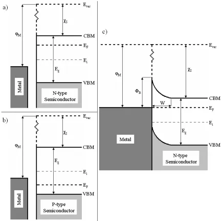
Metal surfaces and semiconductor surfaces both have a wide range of physics associated with them, independent of the other. Before venturing into understanding the theory behind what happens at the interface between a metal and a semiconductor, it is necessary to understand the basic characteristics of both types of surfaces. A band diagram of a metal-semiconductor interface is shown in Figure 2.7, and each of the relevant quantities is indicated in the diagram.
The metal surface is described by the work function of the metal, φM. The work function is the amount of energy necessary to raise an electron from the Fermi level to the vacuum level. The work function is determined from a combination of volume contributions and surface contributions. The volume contribution to the work function is the energy of the electron due to the crystalline lattice of the metal and the interaction of the electron with other electrons. The surface contribution takes into account dipole layers at the metal surface. The dipole layers often exist because the charge distribution around atoms at the metal surface is not symmetric and centers of positive and negative charge do not coincide,
resulting in a dipole layer. Additionally surface reconstructions or relaxations can lead to the formation of surface dipoles. Any change in the electron charge distribution on the surface will change the work function, thus, different crystallographic faces of the same crystal have varying work functions due to varying magnitudes of their dipole layers [81].
The semiconductor is defined by the presence of the band gap in the density of states. The width of the band gap, Eg, separates the valence band maximum (VBM) from the
between the CBM and the energy of the vacuum level (Evac) is also known as the electron affinity, χS, which is the difference in energy between an electron at the CBM and an electron at rest outside the surface of the semiconductor. For any non-zero temperature, there is a finite probability that electrons will be able to be excited into the conduction band. If states within the conduction band are occupied, then conduction is possible.
2.5.2. Schottky Barrier
Once the metal and semiconductor surfaces are brought into intimate contact, the electric fields in the two materials cause a transfer of electrons across the interface, leading to an alignment of the Fermi levels of the metal and semiconductor. While this has no
significant effect on the electronic structure of the metal, the same cannot be said for the semiconductor. When the semiconductor Fermi level aligns with the Fermi level of the metal, the band structure shifts due to internal electrical fields causing the bands to bend up or down, depending on the doping type of the semiconductor and its relationship to the Fermi level of the metal, as shown in Figure 2.7(c). This band bending leads to a barrier to
tunneling across the interface, known as the Schottky barrier. The band bending also leads to the formation of a region of uncompensated donors (or acceptors in p-type semiconductors) next to the metal because ND (or NA) is many orders of magnitude less than the density of electrons in the metal. This region of uncompensated donors (or acceptors) is known as the depletion region and it has a width, W [81].
ΦBn= φM – χS. (2.5.1) Similarly, for a p-type semiconductor,
ΦBp = (Eg + χS) – φM. (2.5.2)
However, the only substrates used in the studies presented in this dissertation were n-type silicon, therefore, for the remainder of this discussion, only the n-type barrier height will be considered. Thus, from this point, ΦBn = ΦB.
2.5.2.1. Models of Schottky Barrier Formation
While the basic physics describing the formation of the Schottky barrier are presented above, several different models have been created to further explain the formation and
behavior of the Schottky barrier, particularly as it relates to the full range of materials.
2.5.2.1.1. Schottky-Mott Model
2.5.2.1.2. Metal-Induced Gap States (MIGS) Model
The Metal-Induced Gap States (MIGS) model was developed by Heine in the 1960’s [87]. The MIGS model states that the electronic wave functions of the metal atoms do not simply cease to exist at the surface of the metal. Rather, they exponentially decay as
predicted by quantum mechanics. However, when the metal is brought into contact with the semiconductor, the metallic wave functions do not simply decay into free space, they penetrate into the semiconductor as far as the Thomas-Fermi screening length. In the semiconductor, the tails of the metallic wave functions induce electronic states in the band gap at energies below the Fermi level.
The induced electronic states form a continuum with a charge neutrality level (CNL), ECNL, which pins the Fermi level if the density of gap states is high enough. It has been shown that this is not the case and the screening potential of the MIGS continuum is limited [99].A semi-empirical formula has been derived for the Schottky barrier height that accounts for this limited screening (for an n-type semiconductor) [85-86],
ΦB = (EC – ECNL) + S(φM – ΦCNL), (2.5.3) where φM is the metallic work function, ΦCNL is the energy location of the CNL (ECNL) from the vacuum level, and S is the slope factor,
S =
(
CNL)
i MIGS i E D q δ ε ε 0 2 1 1 +, (2.5.4)
![Figure 2.3: (a) Basic operational principle of the AFM [26]. (b) Basic schematic of c-AFM measurements presented in Chapter 4](https://thumb-us.123doks.com/thumbv2/123dok_us/1399018.1172604/77.612.97.538.84.624/figure-basic-operational-principle-schematic-measurements-presented-chapter.webp)

![Figure 2.5: CITS images of occupied Si(111):7×7 surface states. (a) Adatom state at -0.35 V, (b) dangling bond state at -0.80 V, (c) backbond state at -1.7 V [49]](https://thumb-us.123doks.com/thumbv2/123dok_us/1399018.1172604/79.612.91.387.69.631/figure-images-occupied-surface-states-adatom-dangling-backbond.webp)
![Figure 2.8: Saddle point potential due to Schottky barrier height inhomogeneity model [108]](https://thumb-us.123doks.com/thumbv2/123dok_us/1399018.1172604/82.612.195.426.71.296/figure-saddle-point-potential-schottky-barrier-height-inhomogeneity.webp)