Analysis of Hexagonal Wide Slot Antenna with Parasitic Element
for Wireless Application
Barun Kumar, Bhupendra K. Shukla*, Ajay Somkuwar, and Om P. Meena
Abstract—A rigorous analysis of hexagonal slot with electromagnetically coupled parasitic element is presented in this article. The wide band feature of the antenna highly depends on the shape and location of the parasitic element and tuning stub. It is found that tuning and overlapping of resonating modes at lower frequency band are mainly achieved by parasitic element. The proposed antenna exhibits the bandwidth of 120.83% from 1.45 to 5.8 GHz for S11 < −10 dB. The parameters of the antenna and circuit model are studied. The role of individual resonators in circuit modeling is also explained. Series of equations for lower cutoff frequency and other resonating frequencies are deduced after inspecting the surface current distribution. At frequencies 2.27, 4.17, and 5.2 GHz, the simulated and measured far fields are compared.
1. INTRODUCTION
Basically, wide slot antenna possesses large number of resonating modes. In fact, the density of mode increases as frequency increases. Before effective tuning of resonating modes, wide frequency response and good impedance matching cannot be realized. The conceptual view of the non-overlapped modes is shown in Figure 1(a). The impedance of some modes likefr2,fr4,fr6are also not matched. Combination of tuning stub and parasitic element with wide slot antenna and overlapping the resonating modes (fr1,
fr2, fr3, fr4, fr5, fr6 and fr7), and wideband frequency response of the antenna can be achieved. Figure 1(b) displays the overlapping of resonating modes. Wide slot antennas become popular in wireless communication industry because of their wide impedance bandwidth, radiation pattern, and planar geometry. In addition, these antennas possess some virtues like low cost, light weight, and ease of integration with other microwave devices [1–4]. The main demerit of conventional planar antennas is narrow fractional bandwidth that restricts their wide use. The shape and area of slot play crucial role in planar antennas. Indeed, slot affects the current distribution and position of resonating modes. They also modify effective capacitance, inductance, and the phase velocity (vp = 1
√
LC) of the resonating modes (T M10, T M01, T M12 and T M20) [5–8]. A microstrip fed rotated slot antenna exhibits the
bandwidth of 48.8% and occupies the frequency span from 3.4 to 5.6 GHz for S11 < −10 dB [9]. The combination of simple feed line and wide slot does not show good impedance bandwidth. To improve the performance of the antenna, combination of wide slot and tuning stub can be used. Here, the tuning stub is responsible for impedance bandwidth and matching in the entire operating frequency band. Moreover, a wide slot antenna with a fan-shaped tuning stub is proposed which covers the frequency band from 1.55 to 5.66 GHz for S11 < −10 dB [10]. Some more reported tuning stubs are circular, elliptical, and fork-shaped [11–15]. The bandwidth of a wide slot antenna is critically affected when size of ground plane is comparable to slot size. To adjust the impedance matching in the wide frequency range, parasitic element is embedded. Shinde fabricated pentagonal slot with same shaped parasitic
(a) (b)
Figure 1. S11 characteristic of the slot loaded antenna. (a) Before tuning. (b) After tuning of modes.
element and achieved the fractional bandwidth of 77.72% for S11 < −10 dB [16]. Moreover, 108.7% impedance bandwidth was reported by Jan and Wang. They designed a rhombus slot antenna with a pair of parasitic elements [17]. A hexagonal slot with a hexagonal parasitic patch was reported by Rani and Pandey. This antenna covered the frequency span from 3.71 GHz to 12.15 GHz with one frequency notched band [18].
In this communication, an analysis of a hexagonal wide slot antenna is presented and discussed. We have chosen an irregular hexagonal slot because of following reasons 1) The tuning of the area of the slot, 2) Tuning of mutual coupling with parasitic element, 3) Tuning of impedance bandwidth. Section 2 describes the physical structure and parameters of the antenna. The development of the antenna and mathematical modeling are included in Section 3. The circuit behavior of the antenna and effect of elements are studied in Section 4. The impact of parameters on frequency response of the antenna is investigated in Section 5. The experimental results are discussed in Section 6. The frequency formulation of resonating frequencies and lower cutoff frequency are described in Section 7. The far field results are compared in Section 8.
2. ANTENNA CONFIGURATION
Figure 2 illustrates the physical structure of the hexagonal wide slot antenna with parasitic element which is designed on a commercially available FR-4 substrate. It is positioned on the azimuthal, and
Z axis is perpendicular to the tuning stub. The properties of chosen substrate are dielectric constant of 4.4, thickness of 1.6 mm, and loss tangent 0.02. The overall volume of antenna is 50 mm × 50 mm
Figure 2. The physical structure of hexagonal wide slot antenna with parasitic element.
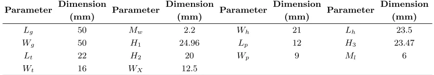
Table 1. Structural parameters and dimensions of hexagonal shaped wide slot antenna.
Parameter Dimension
(mm) Parameter
Dimension
(mm) Parameter
Dimension
(mm) Parameter
Dimension (mm)
Lg 50 Mw 2.2 Wh 21 Lh 23.5
Wg 50 H1 24.96 Lp 12 H3 23.47
Lt 22 H2 20 Wp 9 Ml 6
Wt 16 WX 12.5
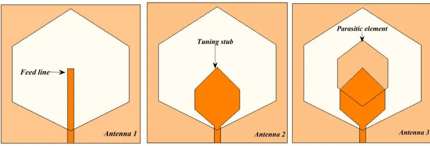
3. EVOLUTION OF THE HEXAGONAL WIDE SLOT ANTENNA
Figure 3 exhibits the development of the proposed antenna. As shown in Figure 3, a tuning stub and parasitic element are integrated in the consecutive steps. The comparedS11characteristic of antennas is displayed in Figure 4. Antenna 1 consists of feed line and irregularly shaped hexagonal slot. It exhibits the bandwidth (BW(%) = 200∗(fh−fl)/ (fh+fl)) of 29.70% from 2.15 to 2.9 GHz for S11<−10 dB with one resonating frequency at 2.48 GHz. This resonating frequency is produced due to feed line which can be estimated by following equations.
Lf eed=Ml+Lt∼= 28 mm (1)
ff eed= C
Lf eed√εr
∼
= 300
28∗√4.4 ∼= 2.57 GHz (2) where Lf eed is the length of feed line in antenna 1, and ff eed is the frequency generated by feed line. In antenna 2, a tuning stub is integrated with the feed line. Tuning stub plays two role 1) improves impedance matching at higher frequency band 2) produces new resonance frequencies. The fundamental frequency due to tuning stub can be computed by following steps [19, 20].
a) By equating the area of circle and irregular hexagonal patch
πr2
c = Ah (3)
rc = √Ah/π (4)
Figure 3. Development of hexagonal wide slot antenna with parasitic element.
Figure 4. Development of hexagonal wide slot antenna with parasitic element.
b) Calculation of effective radius and resonance frequency
rceff = (rc)
1 + 2h
πεrrc
ln
rc 2h
+ (1.41εr+ 1.77) 1/2
(5)
ft= 1.8412∗C0
2∗π∗rceff ∗√εr (6)
whererceff andεrare the effective radius of circle and dielectric constant of the substrate. The calculated value of rceff is 9.72 mm, and computed value of ft is 4.32 GHz. Antenna 2 covers the frequency band from 2.57 to 6 GHz forS11<−10 dB. In the next step, a parasitic element is added which is responsible for impedance matching in lower frequency band. This parasitic element changes the capacitance of the antenna and enhances the mutual coupling between wide slot and tuning stub. Antenna 3 exhibits the bandwidth of 119.14% from 1.52 to 6 GHz for S11 < −10 dB with four resonating frequencies at 1.66, 2.27, 4.25, and 6 GHz.
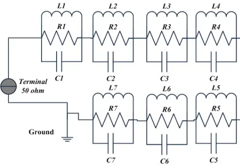
4. EQUIVALENT CIRCUIT MODEL
Figure 5. Circuit model of the rectangular patch antenna.
The values of L1,C1, and R1 can be calculated by the following equations.
C1 = LW ε0εe 2h cos
2πx0 L
(7)
R1 = Q
ω2 rC1
(8)
L1 = 1
C1ω2 r
(9)
Q = c
√
εe
4fh (10)
where L and W are the length and width of the patch. x0 and εe are the feed location and effective permittivity of the substrate. Q and h are the quality factor and height of the substrate, respectively. The input impedance of the rectangular patch antenna is given by
Zin =jωLprobe+ 1 1
R1 +
1
jωL1 +jωC1
(11)
A patch antenna exhibits a narrow impedance bandwidth. The above mentioned circuit model resonates only at single frequency. To create more resonating frequencies, a slot is embedded on patch which modifies the position of resonating frequencies. A wideband characteristic of the antenna is achieved by the overlapping of the resonating frequencies (see Figure 1). The circuit model of proposed hexagonal wide slot antenna is displayed in Figure 6 which is the cascaded connection of the seven parallel RLC circuit. The elements of the first and second resonators control the position of the lower cutoff and
first resonating frequencies. The impedance matching and position of the second resonant frequency are controlled by third and fourth resonators. The elements of the 5th resonator change the position of the third resonant frequency as well as impedance at mid and higher frequency bands. The elements of the 6th and 7th resonators control the impedance matching at higher frequency band. The total impedance of the proposed circuit model can be computed by the equation below.
Zin =
7
i=1
1 1
Ri +
1
jωLi +jωCi
(12)
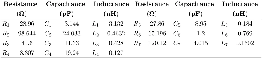
The values of all elements are listed in Table 2. The comparison of reflection coefficient characteristics is shown in Figure 7.
Table 2. Obtained values ofR,L,C.
Resistance (Ω)
Capacitance (pF)
Inductance (nH)
Resistance (Ω)
Capacitance (pF)
Inductance (nH)
R1 28.96 C1 3.144 L1 3.132 R5 27.86 C5 8.95 L5 0.184
R2 98.644 C2 24.033 L2 0.4632 R6 65.196 C6 1.2 L6 0.769
R3 41.6 C3 11.33 L3 0.428 R7 120.12 C7 4.015 L7 0.1602
R4 8.307 C4 19.24 L4 0.127
Figure 7. Comparison of frequency responses obtained from CST and circuit simulation.
5. TUNING OF PARAMETERS 5.1. Effect of Width of Feed Line
11
The simulated S11 characteristic vs frequency for different values ofLt and Wt is depicted in Figure 9. For Lt >24 mm, the overlapping area with parasitic element and effective capacitance of the antenna increase. Due to this, the impedance matching degrades at higher frequency band. Moreover, the width of tuning stub (Wt) critically affects impedance matching in the entire operating frequency band. This parameter also changes the effective capacitance of the antenna and mutual coupling between wide slot and tuning stub.
Figure 8. SimulatedS11 versus frequency for different value ofMw of the proposed antenna.
Figure 9. SimulatedS11 versus frequency for different value ofLt and Wt of the proposed antenna.
5.3. Impact of Parasitic Element on S11 Characteristic
Figure 10. Simulated S11 versus frequency for different value ofLp and Wp of the proposed antenna.
Figure 11. Simulated S11 versus frequency for different value ofLy and Wh of the proposed antenna.
and capacitance of the antenna. The position of resonating frequencies is changed due to the change in phase velocity (vp = 1
√
LC) of them. It is noticed that length of parasitic element controls the impedance matching at mid and higher frequency bands whereas the width of parasitic element does not affect the fractional bandwidth of the antenna significantly.
5.4. Impact of Hexagonal Wide Slot on S11 Characteristic
improved. The width of the slot affects the position of lower cutoff frequency and increases the path length of current vectors which are scattered around the wide slot.
6. RESULTS AND DISCUSSION
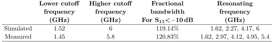
After numerical investigation of the proposed antenna, it is fabricated on an FR-4 substrate. The prototype of proposed antenna is illustrated in Figure 12. The frequency response of fabricated antenna is measured through Vector network analyzer N9923A in frequency range 1 to 6 GHz. The comparedS11 characteristic is displayed in Figure 13. This antenna exhibits five resonant frequencies and 120.83% fractional bandwidth. Table 3 represents the performance characteristics of the hexagonal wide slot antenna in terms of bandwidth and resonant frequencies. It is noticed that the measured and simulated reflection coefficient characteristics do not match at higher frequency band due to various reasons 1) connector and conductor loss, 2) variation of dielectric constant, 3) effect of ground plane which shifts the resonant frequency.
Figure 12. Schemetic view of fabricated hexagonal wide slot antenna.
Table 3. Bandwidth and resonating frequency of the hexagonal wide slot antenna.
Lower cutoff frequency
(GHz)
Higher cutoff frequency
(GHz)
Fractional bandwidth For S11<−10 dB
Resonating frequency
(GHz)
Simulated 1.52 6 119.14% 1.62, 2.27, 4.17, 6
Measured 1.45 5.8 120.83% 1.62, 2.97, 4.12, 4.95, 5.4
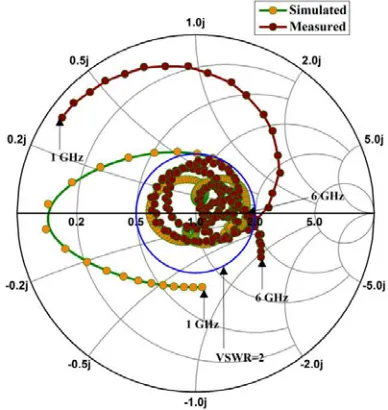
Figure 14 illustrates the compared input impedance characteristic of the antenna. It is noticed that multiple loops are formed inside of the VSWR circle. Formation of loop confirms the overlapping and mutual coupling of the modes.
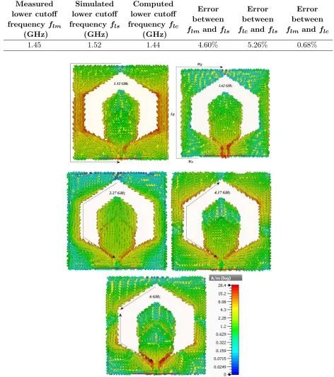
7. SURFACE CURRENT DISTRIBUTION
At frequencies 1.52, 1.62, 2.27, 4.17, and 6 GHz, the symmetric distribution of current vectors is displayed in Figure 15. It is noticed that current distribution becomes complicated at higher frequencies due to the presence of higher order modes. The lower cutoff frequency (1.52 GHz) is produced due to edges of the ground plane. The resonant length and lower cutoff frequency are computed by following equations
Lf =Lg+Wg 2 +
Wg
2 ∼= 100 mm (13)
fl= C
Lf√εr
∼
= 300 100∗√4.4
∼
Figure 13. The compared reflection coefficient characteristic versus frequency plots.
Figure 14. Compared input impedance of hexagonal wide slot antenna with parasitic element.
where εr is the dielectric constant of the substrate, and fl is the lower cutoff frequency. Lf is the resonant length for lower cutoff frequency. The estimated error between calculated, simulated, and measured lower cutoff frequencies is listed in Table 4.
After investigating the surface current distribution at frequency 1.62 GHz, it has been noticed that this frequency is generated due to edges of the ground plane. Frequency formulation for the first resonant frequency is given below
L1=Lg+Wg
Measured lower cutoff frequency flm
(GHz)
Simulated lower cutoff frequency fls
(GHz)
Computed lower cutoff frequency flc
(GHz)
Error between
flmand fls
Error between
flc and fls
Error between
flm and flc
1.45 1.52 1.44 4.60% 5.26% 0.68%
Figure 15. Schematic of surface current distribution at lower cut off frequency and other resonating frequencies.
f1= C
L1√εr
∼
= 300
87.5∗√4.4 ∼= 1.64 GHz (16)
simulated, and measured values of f1 are nearly equal. The current vectors are also scattered on the boundary of the hexagonal wide slot. A resonance frequency due to wide slot can be estimated by following equations
Lperimeter=H1+H2+H3∼= 68.43 mm (17)
f2= C
Lperimeter√εr
∼
= 300 68.43∗√4.4
∼
= 2.09 GHz (18)
whereLperimeter is the half perimeter of the hexagonal wide slot. An error of 7.29% is computed between calculated and simulated second resonant frequencies. To minimize the error, an effect of fringing is considered in the following equations.
Ahexagonal =Arectangular =Lrect∗Wrect (19)
where Ahexagonal and Arectangular are the areas of hexagonal and rectangular slots, respectively. Lrect andWrectare the length and width of the rectangular slot (see Figure 16). Here, the length of hexagonal slot is equal to the length of rectangular slot.
1764 = 44∗Wrect (20)
The calculated value of Wrect is 40.09 mm. The effective dielectric constant and fringing field length can be computed by following equations.
εeff = εr
+ 1 2 +
εr−1 2
1 + 12∗ h
Wrect
−0.5
∼
= 4.09 (21)
Lf ringing = h∗0.412∗(εr+ 0.3)∗(
Wrect
h + 0.258)
(εr−0.258)∗(Wrect
h + 0.8)
= 0.7393 mm (22)
The effective length of the slot and modified second resonant frequency are estimated by below equations.
Leff =Lrect−2∗Lf ringing ∼= 66.9514 mm (23)
f2 = C
Leff
√
εeff ∼=
300 66.9514∗√4.09
∼
= 2.22 GHz (24)
At frequency 4.17 GHz, two half wavelength variations of current vectors are investigated along the wide slot. This frequency is nearly equal to the second harmonics of 2.27 GHz. It is noticed that the broad frequency response near 4.2 GHz range is achieved after overlapping of two resonant frequencies 1) second harmonics of wide slot 2) fundamental frequency of tuning stub. The fundamental frequency produced by parasitic element is 3.87 GHz which can be calculated by Equations (3) to (6). At 6 GHz, three half wavelength variation of the current vectors has been investigated along the wide slot. This frequency is nearly equal to the third harmonics of 2.27 GHz.
At frequencies 2.27, 4.17, and 5.2 GHz far field has been simulated and measured in E plane and H plane. The comparison of far field patterns of proposed antenna is displayed in Figure 17. At frequency 2.27 GHz, the eight-shape pattern is investigated in E plane. In simulation, directional pattern is obtained in H plane which does not match the measured result. The reason may be radiating nature of coaxial cable at lower frequencies. At frequency 4.17 GHz, the shape of pattern almost matches the measured pattern in both planes. It can also be noticed that at 4.17 GHz, the pattern shape is changed in both planes. This occurs due to existence of some higher order modes. At frequency 5.2 GHz, the patterns in both planes are changed due to the presence of higher order modes. As frequency increases the higher order modes also increases (see Figure 15).
(a)
(b)
(c)
9. CONCLUSION
A hexagonal slot antenna with parasitic element has been investigated. The wide frequency response characteristic of this antenna is achieved by selecting proper dimension of the parasitic element and tuning stub. These two elements also control the impedance matching in the entire frequency band. For investigation, the circuit model is also proposed, and it is found that the position of resonant frequencies and impedance matching depend on the circuit elements. This antenna covers the bandwidth of 120.83% from 1.45 to 5.8 GHz forS11<−10 dB. A series of equations have been deduced for resonating frequencies. This frequency formulation is achieved after inspecting the surface current distribution. At frequencies 2.27, 4.17, and 5.2 GHz, the far field patterns are investigated. It is noticed that the shape of the pattern is changed due to the presence of higher order modes.
REFERENCES
1. Tang, M. C., R. W. Ziolkowski, and S. Xiao, “Compact hyper band printed slot antenna with stable radiation properties,”IEEE Transactions on Antennas and Propagation, Vol. 62, No. 6, 2962–2969, June 2014.
2. Shukla, B. K., N. Kashyap, and R. K. Baghel, “A novel design of Scarecrow-shaped patch antenna for broadband applications,” International Journal of Microwave and Wireless Technologies, Vol. 10, No. 3, 351–359, 2018.
3. Purohit, P., B. K. Shukla, and D. K. Raghuvanshi, “A novel design of hybrid open slot antenna with parasitic element for wideband applications,”Progress In Electromagnetics Research C, Vol. 90, 95– 107, 2019.
4. Eskandari, H. and M. N. Azarmanesh, “Bandwidth enhancement of a printed wide-slot antenna with small slots,”AEU-International Journal of Electronics and Communications, Vol. 63, 896–900, 2009.
5. Harackiewicz, F. J., A. Alazza, and H. R. Gorla, “Very compact open-slot antenna for wireless communication systems,” Progress In Electromagnetics Research Letters, Vol. 51, 73–78, 2015. 6. Kumar, B., B. K. Shukla, A. Somkuwar, and D. K. Raghuvanshi, “A study of hybrid wide slot
antenna with hybrid parasitic element for wideband applications,” Progress In Electromagnetics Research C, Vol. 89, 27–38, 2019.
7. Deshmukh, A. A. and K. P. Ray, “Formulation of resonance frequencies for dual-band slotted rectangular microstrip antennas,”IEEE Antennas and Propagation Magazine, Vol. 54, 78–97, 2012. 8. Deshmukh, A. A. and K. P. Ray, “Analysis of broadband variations of U-slot cut rectangular
microstrip antennas,” IEEE Antennas and Propagation Magazine, Vol. 57, 181–193, 2015.
9. Jan, J. Y. and J. W. Su, “Bandwidth enhancement of a printed wide-slot antenna with a rotated slot,” IEEE Transactions on Antennas and Propagation, Vol. 53, 2111–2114, 2005.
10. Yao, F. W., S. S. Zhong, W. Wang, and X. L. Liang, “Wideband slot antenna with a novel microstrip feed,” Microwave and Optical Technology Letters, Vol. 46, 275–278, 2005.
11. Zhong, Y. W., G. M. Yang, and L. R. Zheng, “Planar circular patch with elliptical slot antenna for ultrawideband communication applications,” Microwave and Optical Technology Letters, Vol. 57, 325–328, 2015.
12. Arya, A. K.. R. S. Aziz, and S.-O. Park, “Planar ultra-wideband printed wide-slot antenna using fork-like tuning stub,” Electronics Letters, Vol. 51, No. 7, 550–551, 2015.
13. Dastranj, A. and H. Abiri, “Bandwidth enhancement of printed E-shaped slot antennas fed by CPW and microstrip line,”IEEE Transactions on Antennas and Propagation, Vol. 58, 1402–1407, 2010.
14. Li, P., J. Liang, and X. Chen, “Study of printed elliptical/circular slot antennas for ultrawideband applications,” IEEE Transactions on antennas and Propagation, Vol. 54, 1670–1675, 2006.
enhancement for multiband wireless applications,” AEU-International Journal of Electronics and Communications, Vol. 69, 1489–1494, 2015.
17. Jan, J. Y. and L. C. Wang, “Printed wideband rhombus slot antenna with a pair of parasitic strips for multiband applications,”IEEE Transactions on Antennas and Propagation, Vol. 57, 1267-1270, 2009.
18. Rani, R. B. and S. K. Pandey, “A parasitic hexagonal patch antenna surrounded by same shaped slot for WLAN, UWB applications with notch at vanet frequency band,” Microwave and Optical Technology Letters,Vol. 58, 2996–3000, 2016.
19. Ray, K. P., M. D. Pandey, and S. Krishnan, “Determination of resonance frequency of hexagonal and half hexagonal microstrip antennas,”Microwave and Optical Technology Letters, Vol. 49, 2876– 2879, 2007.
20. Ray, K. P. and G. Kumar, “Determination of the resonant frequency of microstrip antennas,”Microwave and Optical Technology Letters, Vol. 23, 114–117, 1999.
21. Singh, A., M. Aneesh, and J. A. Ansari, “Analysis of microstrip line fed patch antenna for wireless communications,”Open Engineering, Vol. 7, 279–286, 2017.
22. Pawar, S. S., M. Shandilya, and V. Chaurasia, “Parametric evaluation of microstrip log periodic dipole array antenna using transmission line equivalent circuit,”Engineering Science and Technology, an International Journal, Vol. 20, 1260–1274, 2017.
23. Singh, A., M. Aneesh, K. Kamakshi, and J. A. Ansari, “Circuit theory analysis of aperture coupled patch antenna for wireless communication,”Radioelectronics and Communications Systems, Vol. 61, 168–179, 2018.
24. Devesh, T., J. A. Ansari, M. G. Siddiqui, and A. K. Saroj, “Analysis of modified square Sierpinski Gasket fractal microstrip antenna for wireless communications,” AEU-International Journal of Electronics and Communications, Vol. 94, 377–385, 2018.