Introduction
• Conventional optical receiver is not capable of handling rapid change of signal amplitude and clock phase alignment.
• Burst mode receiver is designed to handle such busty nature of packets.
• The receiver can quickly extract the decision threshold and determine the signal phase from a set of overhead bits placed at the beginning of each packet burst.
• Two NW terminals have impact on Burst mode receiver.
• Passive optical network (PON)
Passive Optical Networks (PONs)
• A passive optical network (PON) uses CWDM over a single bidirectional optical fiber.
• Only passive optical components guide traffic from the central office to the customer premises and back to the central office.
• In the central office, combined data and digitized voice are sent downstream to customers by using a 1490-nm wavelength.
• The upstream (customer to central office) uses a 1310-nm wavelength.
• Video services are sent downstream using a 1550-nm wavelength.
Active PON Modules
• The optical line termination (OLT) is located in a central office and controls the bidirectional flow of information across the network.
• An optical network termination (ONT) is located directly at the customer premises.
• The ONT provides an optical connection to the PON on the upstream side and to interface electrically to the local customer equipment.
• An optical network unit (ONU) is similar to an ONT, but is located near the customer and is housed in an outdoor equipment shelter.
Burst mode receiver
• Burst nature of the arrived packet is represented by amplitude and phase variation of the arrived packet from different ONTs
Unit: 7
WDM OPTICAL NETWORKS
• Considerable increase in traffic became a driving force for WDM and its evolution into dense WDM (DWDM).
• WDM refers to the technology of combining multiple wavelengths onto the same optical fiber.
• Each wavelength is a different channel.
• At the transmitting end, there are W independent transmitters. Each transmitter Tx is a light source, such as a laser, and is independently modulated with a data stream. The output of each transmitter is an optical signal on a unique wavelength λi , i = 1, 2, . . . , W.
• WDM: ~200 GHz spacing
Basic Principle
• WDM components are nothing but star couplers.(Wavelength divider or combiner)
• Principle role is to combine the powers from N inputs and divide the equally among M output ports.
• Techniques: Fused fibers, gratings, micro optic techniques, Integrated optics schemes.
• Example: 7×7, 1×19, 4×4 star couplers.
• For a N×N star coupler,
• Splitting Loss =
• Excess Loss =
10log10(𝑁
10log10 𝑃𝑖𝑛
𝑗=1 𝑀
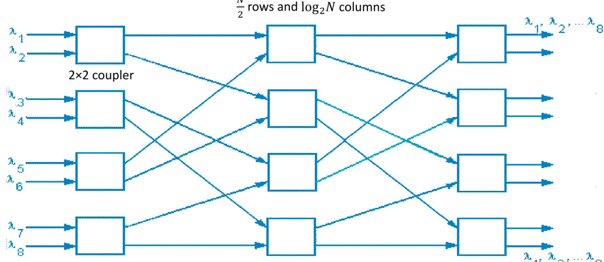
Realization of 8×8 star coupler using 2×2 coupler
Simplified structure
Fig. Realization of 8×8 star coupler using 2×2 3-dB coupler 2×2 coupler
𝑁
Simple calculation!!!
• No of 3-dB coupler required for a N×N star coupler
• If the fraction of power traversing is 𝐹𝑇 (0<𝐹𝑇<1), then fraction of loss power = (1-𝐹𝑇)
• Excess loss =
• Splitting loss = 10log(N)
• Total loss = −10log10(𝐹𝑇log2𝑁) + 10log10𝑁
=
𝑁𝑐 = 𝑁
2 . log2𝑁
−10log10(𝐹𝑇log2𝑁
−10log10 𝐹𝑇
log2𝑁
Problem:
• Consider a commercially available 32×32 single mode coupler made from cascading 3 dB fused fiber 2×2 couplers, where 5% of the power is lost in each element. Calculate total loss.
Need for Optical Isolator
• Optical isolators are devices that transmit light only in one direction. • If back-reflected and scattered light enters into the laser, the lasing
process will fluctuate and the output power of the laser will fluctuate. • But in fiber optic networks, most of the reflections are harmful to the
stability of the system which is especially true for lasers and optical amplifiers.
• Optical isolators play a vital role in fiber optic systems by stopping back-reflection and scattered light from reaching sensitive
Limitations of Polarization dependent Isolator
• Polarization state of the output beam of the laser should be exactly aligned to the transmission axis of the input linear polarizer.
• Any mismatch in the polarization state gives insertion loss.
Polarization independent Isolator – How it works?
• Regardless of the polarization state of the input beam, the output beam will propagate through the fiber with zero insertion loss.
• The reflected beam will be isolated from the source.
• It replaces the two linear polarizers using Birefringent wedge or crystal.
• ‘o’ – Ordinary Ray, ‘e’- Extra-ordinary Ray
Polarization independent Isolator (Contd..)
• The first wedge crystal splits the input beam into ‘e’ and ‘o’ rays which are linearly polarized and orthogonal to each other.
• Both the rays will be rotated by +45°. Second wedge axis is at 45° relative to first wedge. So the light rays are focused and emerge out from the wedge as single ray.
• For reflected ray the second wedge splits the beam into ‘e’ and ‘o’ ray. Due to Faraday rotator of +45°, ‘e’ ray becomes ‘o’ ray and ‘o’ ray becomes ‘e’ ray.
• The first wedge again separate out the two beams and diverges the rays.
Summary:
Polarization dependent Isolator Polarization independent Isolator
It is dependent on input signal polarization It is independent on input signal polarization
It uses fixed polarizers with specific rotation It uses Birefringent Crystal with specific rotation
Less flexible for usage More flexible for usage
More insertion loss Less insertion loss
MEMS
Introduction
• Micro-Electro-Mechanical Systems or MEMS Technology is a
precision device technology that integrates mechanical elements, sensors, actuators, and electronics on a common silicon substrate through micro fabrication technology.
Micro : Small size, micro fabricated structures
Electro : Electrical Signal/ Control
Mechanical : Mechanical functionality
Systems : Structures, Devices, Systems
• MEMS is also referred to as MST (Microsystems Technology in Europe) and MM (Micromachines in Japan). MEMS with optics is called
Introduction (contd..)
• IC- “Brain” of a system, MEMS- “Sense and limbs” of the brain
• These systems can sense, control and actuate on microscale, and function individually or in arrays to generate effects on macroscale.
• In MEMS devices, a three-dimensional spatial structure is formed on the
substrate and mechanical blocks are formed within that structure, A system is then created by fabricating electrical circuits that drive those mechanical blocks on the same substrate.
• This technology is targeted at devices that range in size from mm down to
General Structure
• In the most general form, MEMS consist of mechanical microstructures, microsensors, microactuators and microelectronics, all integrated onto the same silicon chip.
• Microsensors detect changes in the system’s environment by measuring mechanical, thermal, magnetic, chemical or electromagnetic information or phenomena.
• Microelectronics processes this information and signals the microactuators to react and create some form of changes to the environment.
References:
• WDM Operation: Keiser 4th Ed.
• Isolator : Note is uploaded to website • MEMS technology:
• http://www.engineersgarage.com/articles/mems-technology
• http://www.egr.msu.edu/classes/ece410/mason/files/MEMS%20overview.pdf