Copyright © 2013 IJECCE, All right reserved
Reconfigurable Area & Speed Efficient Decimator Using
DA Algorithm
Rajesh Mehra, Lajwanti Singh
Abstract–Decimator is an important sampling device used
for multi-rate signal processing in wireless communication systems. In this paper, a reconfigurable area & speed efficient multipliers less decimator is presented. DA has been use d to implement the proposed structure taking advantage of embedded LUT based structure of FPGAs. Efficient solution is designed using half band polyphase decomposition FIR structure. The proposed decimator has been designed with MATLAB Simulink and developed verilog code. Simulation is performed using ModelSim and functional verification is carried out using Xilinx synthesis tool (XST)10.1 and implemented on Spartan-3E based 3s500efg320-5 FPGA device. Improvement of 40% in speed and 50% in area has been observed as compared to MAC based approach.
Keywords–DA, Decimator, DSP, FIR, FPGA, LUT, XST.
I. I
NTRODUCTIONDigital signal processing is an area that has rapidly grown in the past 30 years. Advances in digital hardware and digital computers have spurred this growth. Current integrated circuit technology, namely very-large-scale integration (VLSI), made it possible to develop smaller, faster, and cheaper special-purpose digital processing. These circuits made it possible to construct digital systems capable of performing the complex digital signal processing tasks that are usually too difficult or too expensive to be performed by analog circuitry. Today, many of the functions usually performed by analog means are now realized by less expensive and more reliable digital hardware.
ASICs and DSP chips have been the traditional solution for high performance applications, now the technology and the market are imposing new rules. On one hand, high development costs and time-to-market factors associated with ASICs can be prohibitive for certain applications and, on the other hand, programmable DSP processors can be unable to reach a desired performance due to their sequential-execution architecture. In this context, FPGAs offer a very attractive solution that balance high flexibility, time-to-market, cost and performance [1].
FPGAs are essentially arrays of uncommitted logic and signal processing resources. These allow the designer to implement DSP functions using highly scalable, parallel processing techniques. Some of the most common functions performed by almost all DSP chips are Fast Fourier Transforms (FFTs), FIR filters, Interpolators, Decimators etc. Using FPGAs for hardware acceleration in wireless applications offers extensive processing power to realize promised portability of waveforms and reconfigurability [2]. Key advantages of FPGA are:
1) Their architectures are well suited for highly parallel implementation of DSP functions to enhance system performance.
2) User programmability allows designers to trade-off device area vs. performance by selecting the appropriate level of parallelism to implement their functions. By programming the FPGA to use more on-chip resources, designers can achieve higher performance. By using less resources (and accepting a corresponding lower performance), designers can optimize the design for low cost.
3) The other added advantage of FPGAs is its ability to integrate system logic. There are still plenty of resources left to handle traditional FPGA tasks such as the interfaces between other devices on the PC board. Both the system logic and the DSP functions can be implemented in one cost-effective fabric.
For designing efficient architectures for DSP functions (eg. FIR filters), researchers are working since long. Traditionally, the design methods were mainly focused in multiplier-based architectures to implement the Multiply-and- Accumulate (MAC) blocks that constitute the central piece in FIR filters and several DSP functions.
Fig.1. MAC Based Multiplier Implementation [3] This implementation requires MAC blocks, which is expensive in terms of area and is especially critical for high-order filters. This issue has been partially solved with the new generation of low-cost FPGAs that have embedded DSP blocks.
Copyright © 2013 IJECCE, All right reserved coefficients are represented by a combination of powers of
two in such a way that multiplication can be simply implemented with adder/subtractors and shifters [4].
The second type of multiplier-less method involves the use of memories (RAMs, ROMs) or Look-Up Tables (LUTs) to store pre-computed values of coefficient operations. These are called memory-based methods. Distributed Arithmetic (DA) appeared as a very efficient solution especially suited for LUT-based FPGA architectures.
II. DA B
ASEDD
ECIMATORDiscrete time systems with unequal sampling rates at various parts are called multi rate systems. Their function is to alter the rate of the discrete-time signals, by adding or deleting a portion of the signal samples [5]. The rate conversion requirement leads to production of undesired signals associated with aliasing and imaging errors. So some kind of filter should be placed to attenuate these errors. With Decimation, the sample rate of the discrete signal xi[k] can be decreased by the integer factor M. In the simplest case we can take every Mth sample of xi[k].
xo[k] = xi[k ·M]
This is a sampling process and can therefore cause aliasing. To prevent information loss below Fo, we have to reduce the information selectively. This is done by a low pass filter hM[k] of cut off frequency FCM. For the convolution in the time domain a filter sample rate of Fi is needed (Tf = Ti).
FCM = Fo/2 = Fi/2M HM(f) = {1 for FCM≥ │f│
0 for FCM≤ │f│≤ 2 FCM
By removing samples, the average signal energy per
sample is not changed and no amplification in the filter’s
pass band is needed. It is not necessary to filter xi over the whole time axis, since only every Mth sample is needed afterwards. Decimation can be described by the following block diagram:
Fig.2. Decimation process
DALUT Algorithm
DALUT algorithm is an efficient method for computing inner products when one of the input vectors is fixed. It uses look-up tables and accumulators instead of multipliers for computing inner products and has been widely used in many DSP applications such as DFT, DCT, convolution, and digital filters [3]. This technique, first proposed by Croisier is a multiplier-less architecture that is based on an efficient partition of the function in partial
terms using 2’s complement binary representation of data.
The partial terms can be pre-computed and stored in LUTs. The flexibility of this algorithm on FPGAs permits everything from bit-serial implementations to pipelined or full-parallel versions of the scheme, which can greatly improve the design performance.
In FIR filtering, one of the convolving sequences is derived from the input samples while the other sequence is derived from the fixed impulse response coefficients of the filter. This behavior of the FIR filter makes it possible to use DA-based technique for memory-based realization. It yields faster output compared with the multiplier-accumulator-based designs because it stores the pre computed partial results in the memory elements, which can be read out and accumulated to obtain the desired result [6].
The main problem with DA is that the requirement of memory/LUT capacity increases exponentially with the order of the filter, given that DA implementations need 2K
–words (K being the number of taps of the filter).
DALUT Addressing
DALUT Content
Fig.3.The Distributed Arithmetic Look-up Table
III. P
ROPOSEDD
ESIGN& S
IMULATIONA. Polyphase FIR filter
Polyphase decomposition is used to implement parallel processing for decimation. The number of parallel inputs is programmable and can be 2, 4 or 8. Since it is impossible to change dynamically the number of parallel input ports, the port data_in is large enough to accommodate the highest number of parallel inputs. For example, if the input data width is 10 bits and the number
of parallel inputs is 4 then the data_in port’s width will be
Copyright © 2013 IJECCE, All right reserved
B. MATLAB Based Simulation
When a decimation filter is designed, it is important to decide which type of filters will be used and where decimation will occur. Design flow for decimator filter implementation is shown in figure 4. We go through the same design flow to synthesize and simulate the proposed decimator structure.
Fig.4. Decimation Filter Implementation: Design Flow Following steps are followed to implement the proposed structure:
1) Define the filter specifications such as order, filter design, cut-off frequency and sampling frequency. 2) Calculate the filter coefficient using MATLAB FDA
Tool.
3) Apply DA Algorithm on filter Coefficients.
4) Configure the target FPGA, Virtex 2 based 3s500efg320-4 kit for real time debugging.
5) Check the DA Filter coefficients on target FPGA Chip. 6) Configure the target FPGA.
Equiripple based half band polyphase decimator is designed and implemented using MATLAB. Order of the proposed decimator filter is 66 & implementation cost has been calculated in terms & multiplies and MIPS. The Symmetric structure has shown reduced consumed number of multipliers. The Symmetric direct form FIR filter has consumed 50% less multipliers compared to transferred direct form FIR filter for providing cost and area efficiency [8].
In the decimator design MAC unit has been replaced with LUT unit which is proposed multiplier less technique. The size of the LUT grows exponentially with the order of the filter. Here 67 coefficients are divided in two sections with 34 and 33 coefficients respectively to perform using polyphase decomposition. Then 34 coefficients of one part have been processed by using (6 6 6 6 6 4) DALUT partitioning to limit the size of LUTs.
Fig.5. Various Output Response of FIR Polyphase Decimator
Basic form of DA is fully serial, operating on one bit at a time. If the input data sequence is W bits wide, then a FIR structure takes W clock cycles to compute the output. Symmetric and asymmetric FIR structures are an exception, requiring W+ 1 cycle, because one additional clock cycle is needed to process the carry bit of the pre-adders.
0 5 10 15 20
-120 -100 -80 -60 -40 -20 0
Frequency (kHz)
M
ag
ni
tu
de
(d
B
)
Magnitude Response (dB)
Direct-Form FIR Polyphase Decimator
0 0.2 0.4 0.6 0.8 1 1.2 -0.1
0 0.1 0.2 0.3 0.4 0.5
Time (mseconds)
A
m
pl
itu
de
Impulse Response
Direct-Form FIR Polyphase Decimator
0 0.2 0.4 0.6 0.8 1 1.2 0
0.2 0.4 0.6 0.8 1
Time (mseconds)
A
m
pl
itu
de
Step Response
Direct-Form FIR Polyphase Decimator
-1.5 -1 -0.5 0 0.5 1 1.5 2 -1
-0.5 0 0.5 1
Real Part
Im
ag
in
ar
y
P
ar
t
66
Pole/Zero Plot
Copyright © 2013 IJECCE, All right reserved The inherently bit serial nature of DA can limit
throughput. To improve throughput, the basic DA algorithm can be modified to compute more than one bit sum at a time. The number of simultaneously computed bit sums is expressed as a power of two called the DA radix. For example, a DA radix of 2 (2^1) indicates that one bit sum is computed at a time; a DA radix of 4 (2^2) indicates that two bit sums are computed at a time, and so on. To compute more than one bit sum at a time, the LUT is replicated. Processing more than one bit at a time introduces a degree of parallelism into the operation, improving performance at the expense of area.
IV. FPGA S
YNTHESIS& S
IMULATIONThe multiplier based and multiplier less decimator are implemented and synthesized on Spartan-3E based 3s500efg320-5 target device. Reference [3] shows a design in which, the author has designed and implemented a DA based decimator on Spartan-3E based 3s500efg320-4 target device. The design shows 23s500efg320-4% enhancement in speed by saving almost 50% of the resources as compared to MAC based design.
By keeping the same DALUT partioning of 34 coefficients (6 6 6 6 6 4) and modifying the speed grade, better results has been observed. The modelsim based simulated output of the proposed decimator with 16 bit precision is shown in fig.6
.
Fig.6. Simulated Decimator Output Speed Grade: -5
Minimum period: 14.348ns (Maximum Frequency: 63.857MHz) Minimum Input arrival time before clock: 8.997ns
Maximum output required time after clock: 4.040ns Maximum combinational path delay: No path found
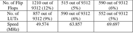
Table 1: Shows the area and speed comparision of MAC based and both DA based techniques. The proposed DA based design shows 40% enhancement in speed by saving almost 50 % of the resouces as compared to MAC based design.
Table 1: Resource utilization Logic
Utilization
Multiplier Approach
Multiplier Less Approach
[3]
Proposed Multiplier Less
Approach
No. of Slices
1055 out of 4656 (22%)
472 out of 4656 (10%)
512 out of 4656 (11%)
No. of Flip Flops
1210 out of 9312 (12%)
515 out of 9312 (5%)
590 out of 9312 (6%) No. of
LUTs
857 out of 9312 (9%)
590 out of 9312 (6%)
552 out of 9312 (5%) Speed
(MHz)
49.574 63.857 69.697
V. C
ONCLUSIONIn this paper, an optimized half band polyphase decomposition technique has been presented to implement the decimator for multi-rate applications. FIR filter of order 66 has been designed using Symmetric direct form structure which shows 50% reduction in multipliers and MIPS as compared to transposed form. Distributed Algorithm has been used to further enhance the speed by taking advantage of LUT structure of target FPGA. The proposed multiplier less approach has shown an improvement of 40% in speed by saving almost 50% resources of target device as compared to multiplier based approach. So DA based symmetric structure is well suited for cost effective implementation of decimator design.
A
CKNOWLEDGMENTThe authors would also like to thank Director, National Institute of Technical Teachers' Training & Research, Chandigarh, India and Director AICE, Jaipur, Rajasthan, India for their inspiration and support throughout this research.
R
EFERENCES[1] Patrick Longa, Ali Miri. “Area-Efficient FIR Filter Design on FPGAs using Distributed Arithmetic”, IEEE International Symposium on Signal Processing and Information Technology, pp: 248-252, 2006.
[2] A. Beygi, A. Mohammadi, A. Abrishamifar, “An FPGA Based Irrational Decimator for Digital Receivers”, IEEE International Conference on Signal Processing and its Application, pp: 1–4, 2007.
[3] Rajesh Mehra, Swapna Devi, “FPGA Based Design of High Performance Decimator using DALUT Algorithm”, ACEEE International Journal on Signal and Image Processing, Volume 1, pp. 9-13, 2010.
[4] M. Yamada, and A. Nishihara, “High-Speed FIR Digital Filter with CSD Coefficients Implemented on FPGA”, inProc. IEEE Design Automation Conference (ASP-DAC 2001), pp. 7-8, 2001.
[5] Rajesh Mehra, Swapna Devi, “Optimized Design of Decimator for Alias Removal in MultirateDSP Applications”, Proceedings of the 10th WSEAS International Conference on Wavelet Analysis and Multirate Systems, pp: 100-103, 2010.
[6] Rajesh Mehra, Ravinder Kaur, “FPGA based Efficient Interpolator design using DALUT Algorithm”,NeTCoM 2010, CSCP 01, pp. 51–62, 2011.
[7] Serigne Mbaye Fallo Dia, Claude Thibeault and François Gagnon, “A Very High Speed and Efficient CIC Decimation Filter Core”, IEEE North- East Workshop on Circuits and Systems, pp. 61-64, 2006.
Copyright © 2013 IJECCE, All right reserved
A
UTHOR’
SP
ROFILEMr. Rajesh Mehra
is currently Associate Professor at National Institute of Technical Teachers’ Training & Research, Chandigarh, India. He is pursuing his PhD from Panjab University, Chandigarh, India. He has completed his M.E. from NITTTR, Chandigarh, India and B.Tech. from NIT, Jalandhar, India. Mr. Mehra has more than 16 years of academic experience. He has authored more than 125 research papers including more than 75 in Journals. Mr. Mehra’s interest areas are VLSI Design, Embedded System Design, Advanced Digital Signal Processing. Mr. Mehra is member of IEEE & ISTE.