Simulation Study of MOSFET Based Drive Circuit Design of
Sensorless BLDC Motor for Space Vehicle
Rajashekar J.S.1 and Dr. S.C. Prasanna Kumar2 1
Associate Professor , Dept. of Instrumentation Technology, Dayananda Sagar College of Engineering, Bangalore and Research scholar Jain University, Bangalore, Karnataka, India. E.mail: [email protected]
2
Professor & HOD, Department of Instrumentation Technology, R.V. College of Engineering, Bangalore, Karnataka, India. E.mail: [email protected]
Abstract – Design, analysis and implementation of an N-channel MOSFET based driver circuit module using discrete components for sensorless brushless direct current (BLDC) motors for space vehicle is discussed in this paper. The prototype module includes a bootstrap circuit to increase the voltage higher than the supply voltage. The driver circuit is simulated using OrCAD software and observed its performance with respect to different gate input frequencies range from 5 Hz to 25 kHz. The BLDC motor includes detecting the rotor position at standstill and a start-up method to drive the motor smoothly without any position sensors. The module includes a current sensor and a general- purpose Microcontroller, which becomes a simple & compact and effective solution for sensor less BLDC motor.
Keywords – Sensorless Brushless DC Motors,
MOSFET based drive circuit, Bootstrap circuit, H-bridge inverter design, level shifter, inductance saliency.
I. Introduction
Brushless Direct Current (BLDC) motors also known as electronically commutated motors is the ideal choice for applications that require high reliability, high efficiency, and high power-to-volume ratio. BLDC motors are capable of providing large amount of torque over a vast speed of ranges. These motors do not have brushes for commutation and they are commutated electronically. Commutation is the act of changing the motor phase currents at the appropriate times to produce rotational torque. In a brush DC motor, the motor assembly contains a physical commutator which is moved by means of actual brushes in order to move the rotor. With a BLDC motor, electrical current powers a permanent magnet that causes the motor to move, so no physical commutator is necessary. These are synchronous motors that are powered by a DC electric source via an integrated inverter, which produces AC electric signal to drive the motor. Brushless motor made of permanent magnet rotor and a fixed armature, eliminates the problems associated with current to the moving armature. An electronic controller replaces the brush commutator
assembly of the brushed DC motor, which continually switches the phase to the windings to keep the motor turning. The controller performs similar timed power distribution by using a solid-state circuit rather than the brush commutator system. BLDC motors have many advantages over brush type DC motors and induction motors. It has better speed - torque characteristics, high dynamic response, high efficiency, long operating life, noiseless operation, higher speed ranges, and more torque per weight, more torque per watt, increased reliability and elimination of ionizing sparks from the commutator & overall reduction of electromagnetic interference. They have been widely used in industries appliances, automotive, and aerospace applications. It is specifically useful in applications where space and weight are critical factors. For aerospace applications, the following factors are considered in electric motor design: Environment, thermal efficiency, weight, volume, life, complexity, torque, speed, torque ripple, power source, envelope, duty cycle, controllability etc..Normally four basic types of electric motors are used in-space applications, AC Induction Motors, Brush Direct Current (BDC) Motors [5], Brushless Direct Current (BLDC) Motors, and Stepper Motors. According the characteristics of each motor they used for different aerospace applications. Brushless direct current motors are the best type of motors for aerospace applications than other type, because of their long life, high torque, high efficiency, and low heat dissipation. Selection of the optimum electric motor for space application, the motor should reliable, efficient & economical. Brushless direct current motors provide the lightest weight alternative for most applications.
N-Channel power MOSFET. The circuit design using Atmega16 microcontroller shown in figure 1.
II. Block Diagram
Figure 1. System Block diagram
The driver circuit with discrete components is specifically designed for power dissipation. There are different methods of drive circuit design for switching a high-side MOSFET. A bootstrap method is choosing for designing the drive circuit. Bootstrap circuit is used to increase the voltage higher than the supply voltage as it is required for high-side switching of MOSFET. Initial phase of the project includes the design of bridge inverter drive circuit for MOSFET [2], suitable for high-side and low-side. The common problem in H-bridge inverter is when MOSFET is connected between the load and VCC supply. The range of gate voltage (VGS) is operated between 10V to 20V for complete turn-on the device. Partial turn-on of the MOSFET due to lower VGS may introduce higher drain to source resistance and dissipating excessive heat when current flows through it. Therefore appropriate gate voltage must be applied to drive the MOSFET into its saturation mode during turn-on state.
III. H Bridge Drive Circuits
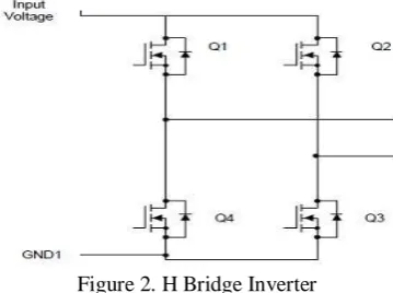
The H bridge inverter MOSFETs arrangement shown in the figure2. This bridge configuration creates two classifications high side (HS) & low side (LS). HS switches refer to Q1 and Q2. These switches have a source connection that is floating voltage during the switching cycle, on this reference changes during the switching cycle. Q3 and Q4 are considered LS switches as their source reference connection is tied to ground and does not change voltage during the switching period. The source voltage Q1 rises, when it turned on, this is usually accomplished by using a bootstrap circuit.
Figure 2. H Bridge Inverter
Figure 3 below shows the design of high side driver circuit consist a level shifter. The level shifter component mainly consists of D5, D6, C1 and D4. The function of the level shifter is to add-up the previously stored voltage across C1 with the +V2 or supply voltage. This can be achieved in order to successfully turn-on the MOSFET
.
Figure 3. High-side driver design
When the +5V input pulse is at low or zero volt, the transistor Q1 is turn-off, consequently turning on the transistors Q3, resulting the MOSFET M1 to turn-off. As Q3 is on, the +15V voltage will charge-up across the capacitor C1. On the other hand, the gate terminal of M1 also connected directly to ground through Q3 and turning off M1. Alternatively, as the input +5V input pulse is at high state, Q1 will turn-on, hence turning off Q3 and turning on MOSFET M1. As Q3 is in off state, the voltage supply of +10V appears at the collector of Q3 and add-up to the voltage +15V previously stored across the capacitor C1. Therefore, the gate voltage of M1 is at 25V with respect to ground, thus M1 is triggered. Design values of resistances R1, R2, R3, R5 used in the high-side MOSFET driver, assuming the supply voltage to be 15V.
is turned off, the 15V supply turns on the low-side MOSFET. When the input is low (0Volts) Q1 is turned off this makes Q2 to be turned on by the supply of 15V, pulling the collector of Q2 and the base of the low-side MOSFET to low level. Thus the low-side MOSFET is turned off. The resistors value R4 calculated from R1, R2&R3.N-channel Low side driver circuit components shown in figure 4.
Figure 4. Low-side driver design
IV. Mosfet Driver Circuit Design
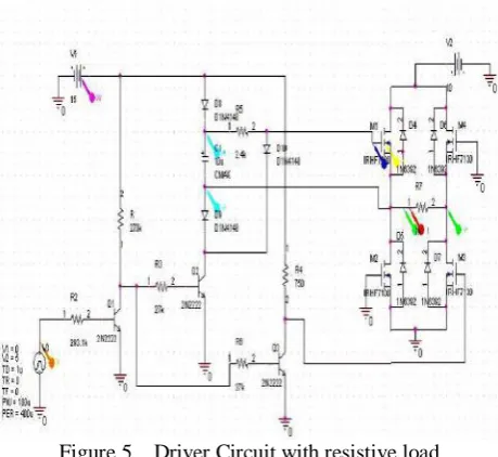
The high-side and the low-side driver are combined to get the complete H-bridge driver circuit as shown in the figure 5 below. Both the high-side as well as the low-side driver circuits are simulated individually to verify their performances, and then combined to form the complete driver circuit. Initially the driver circuit is simulated considering 100Ω resistor as load. The gate drive circuit requirement for high-side gate voltage must be greater than (VDS + Vth).. A low-side switch is a MOSFET that is
connected to the ground-referenced and is not floating. The design of high side and low side drive circuit consist a level shifter. The level shifter components mainly consist of C1, D1, D3 and D4. The function of the level shifter is to add-up the previously stored voltage across C1 with the supply (+Vcc) voltage. This has to be achieved in order to successfully turn-on the MOSFET. However the circuit is simulated for single leg of the three phase bridge inverter for the convenience in simulation as the same circuit would work for all the three legs of the three-phase bridge inverter
.
Figure 5. Driver Circuit with resistive load
When the +5V input pulse is at low or zero volt, the transistor Q3 is turn-off, consequently turn on the Transistors Q1 and Q2, resulting the MOSFET S2 to turn-off. As Q1 is on, the +12V voltage will charge-up across the capacitor C1. On the other hand, the gate terminal of S1 also connected directly to ground through Q1 and turning off S1. Alternatively, as the input +5V input pulse is at high state, Q3 will turn-on, hence turning off Q1, Q2 and turning on MOSFET S2. As Q1 is in off state, the voltage supply of +24V appears at the collector of Q1 through the diode D1 and add-up to the voltage +12V previously stored across the capacitor C1. Therefore, the voltages at point A and B with respect to ground would be 36V leads to triggers S1. From the data sheet of IRHF7130 the specified typical gate threshold voltage (VGS) is 3V, hence any voltage applied across that exceeding 3V.
Figure 6. Driver design with inductive load
V. Experimental Study
Figure 7. Experimental system configurations
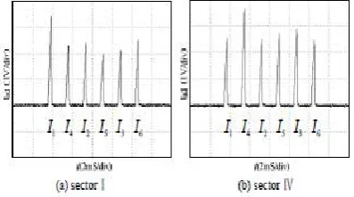
The entire circuit design for experiment to test the drive circuit shown in figure 7. A DC-link current is measured by a current sensing resistor; a sensorless controller is implemented utilizing the proposed method. The system setup developed using 16 bit microcontroller and a current sensor on DC bus. During initial rotor position estimation, the DC-link current has a six-pulse waveform under the effect of six detection voltage vectors, in sequence of V1, V4, V2, V5, V3 and V6 Figure 8 indicate the waveforms of DC-link current when the real rotor position is in two different sectors. It indicates that the differences between six current responses are clear enough to reflect the information of rotor position, and each rotor position sector corresponds to a certain detection voltage vector which generates the maximum current response.
Figure 8 Rotor current responses
Figure. 9 shows the results of the initial rotor position estimation and it reveals that the estimation error is at maximum +/- 15 electrical degrees. Hence it could be said that the estimation resolution is 30 electrical degrees, which is qualified as the commutation signal for BLDC motors
Figure 9. Result of initial rotor position
Figure. 10 show the waveform of DC-link current and the back EMF zero-crossing signal in the starting process. Initial rotor position estimation is repeated several times to ensure the validity of estimation. The back-EMF zero crossing signals are stable before switching to back- EMF and have no mutation after switching. Therefore a successful startup can be achieved.
Figure 10. DC-link current waveform and back EMF cross-zero signal in the starting procedure
VI. Simulation Test Results
Figure 11. Driver circuit with resistive load
Figure 12. Driver circuit with inductive load
From the simulation results we can observe that, the robust voltage applied appears across the load indicating the switching of the MOSFETS properly during different load conditions.
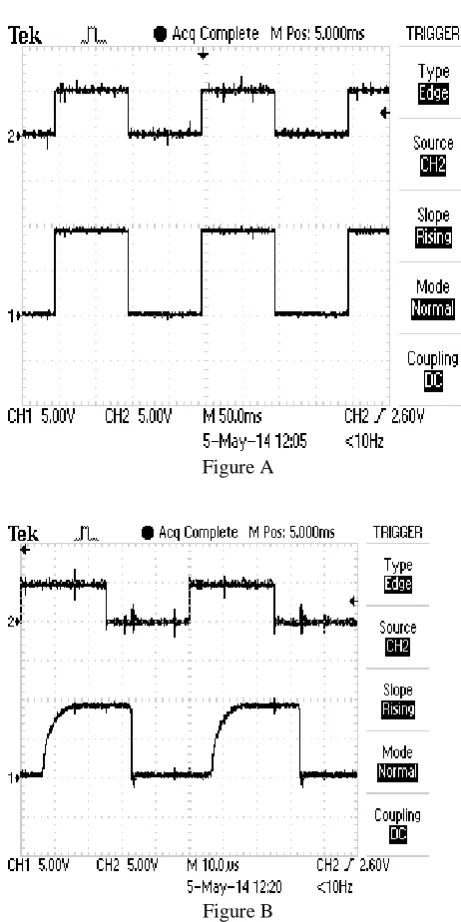
The frequency response test result of the driver circuit shown in Figure A and B
Figure A
Figure B
CH2 represents switching signal voltage at input side of the driver circuit and CH1 indicates the voltage across the 100 Ohm load resistor.
VII. Conclusion
design can be implemented with a low-cost general-purpose microcontroller to provide a simple, compact, and effective solution for BLDC motor drives for various types of application.
References
[1] Mitchell Lee, An Application Note 01, MIC5011 Design Techniques.
[2] B.Maurice, G.Izzo, T.Castagnet, Comparison of MOSFET and IGBT Transistors in Motor Drive applications, an application note
[3] Mr.Abhijit D.Phatak & Mr.Ralph E, Lochen, IXYS Corporation, How to Drive MOSFETs and IGBTd into the 21st century
[4] Shihong Park, Member, IEEE, and Thomas M. Jahns, Fellow, IEEE, IEEE Transactions On Power Electronics, Vol. 20, No. 2, March 2005, A Self-Boost Charge Pump Topology for a Gate Drive High-Side Power Supply.
[5] Nobuyuki Matsui, “Sensorless PM brushless DC
motor drives,” IEEE Trans. Industrial Electronics,
vol.43, pp.300-308, August 1996.
[6] C. C. Chan and Sun Li-qing, “The present status
and future trends of electric vehicles,”
Transactions of China Electrotechnical Society, vol. 9, pp.7–13, September 2005.
[7] G. H. Jang, J. H. Park and J. H. Chang, “Position detection and start-up algorithm of a rotor in a sensorless BLDC motor utilising inductance
variation,” IEE Proc-Eleclr Power Appl, vol. 149,
pp. 137–142, March 2008
[8] Fanlin Meng ; Changhong Fu ; Zhifeng luo
“Research Of Brushless Dc Motor Simulation System Based On RBF-PID Algorithm”
[9] G Prasad, Venkateswara Reddy M, Dr. P V N Prasad, Dr. G Tulasi Ram Das” Speed control of Brushless DC motor with DSP controller using Matlab”
[10] M. Ehsani” Control of BLDC Machines with Improved Performance”
[11] Patrick Fisher, “High Performance Brushless DC Motor Control”