e-ISSN: 2278-067X, p-ISSN: 2278-800X, www.ijerd.com
Volume 11, Issue 12 (December 2015), PP.80-86
An FPGA based Area-Delay Efficient 64-bit Carry
Select Adder Design for High-Speed Applications
Rohit Khare
1, Sandip nemade
21
M.TECH. (V.L.S.I.) Technocrates Institute of Technology, RGTU Bhopal, Madhya Pradesh, India
2
Technocrates Institute of Technology, RGTU Bhopal, Madhya Pradesh, India
Abstract:- In present scenario of VLSI based system designing, efficient area, low power and high speed are the main parameter of design research. The designs must have the desired functionality and also parametric optimized performance. System portability, faster time to market and cost efficiency are the non-technical parameters that effect the life-time performance of the designed system. The low power consumption of VLSI circuit has emerged as the most important design parameter as it directly or indirectly affects the performance of all other technical and non-technical system design parameters. In the present work a Carry-Select-Adder (CSA or CSLA) design with low power combinational design is presented. The design is synthesized and simulated on Field Programmable Gate Array based VLSI hardware for its functional and power performance. The present study presents a comparative speed and power analysis of the proposed work with some existing work. The FPGA based low power analysis is concluded on the basis of the proposed work. The present work is performed using Xilinx Tool.
Keywords:- Carry Select Adder, Half Sum Generator, Half Carry Generator, Carry Select Unit, Dynamic Power.
I.
INTRODUCTION
In the VLSI based system design the main areas of research in present scenario are the low power, reduced size and high speed path logic systems. Since most of the processing are based on the very basic operation of binary addition, the requirement of high speed addition and multiplication is always needed for achieving the desired performance of high speed processors. In the digital system, the speed of addition operation depends on the propagation of carry in the sequential behaviour in the adder circuit. The carry propagates sequentially from single-bit addition logic to the next-bit addition logic and upto the last bit addition. So, this causes a large delay in the adder circuits. The carry propagation operation becomes the main limitation of any adder bit design. The delay parameter becomes more critical in the adders with a larger length of data. This delay is reflected in the complete processing system as the data has to be synchronized throughout the system units that are operating parallel. Many designers and researchers have worked to propose various adder architectures to optimize the carry propagation delay. Many types of adder architectures are available such as Ripple Carry Adder, Carry Look Ahead Adder, Carry Skip Adder, Carry Save Adder and Carry Select Adder. These adders have their own architectures with their own advantages & disadvantages. The present work shows implementation of a 64-bit Carry Select Adder design. The present study shows the power and frequency based analysis of the carry select adder design and a comparison between previously proposed design performances with the present design performance. The different sections of the proposed work are arranged as follows: Section II presents a concise literature survey of the related work and its applications. Section III describes the architecture of 64-bit carry select adder design and the building blocks of the design. Section IV presents the simulation and synthesis results of the work performed in this paper. Section V presents the conclusion based on the present work. And in the last all the references are mentioned.
An FPGA based Area-Delay Efficient 64-bit Carry Select Adder Design for High-Speed Applications
each summation operation and, 1-AND Gate and 1-OR gate in each carry-out operation. An optimized delay and area based design of 16-bit, 32-bit and 64-bit CSLA adder is proposed and compared with the conventional design in [5, 6]. Reference [7] presents an analysis of conventional CSLA and Binary to Excess-1 Converter (BEC) CSLA. This reference presents an innovative 16-bit CSLA architecture that replaced the BEC using D-latch.
A simple and efficient gate-level modification in the architecture of carry-select-adder is proposed in [8] to show a significant reduction in the area and the power of the conventional CSLA design. This paper replaced the ripple-carry-adder in the conventional architecture, with Cin=‟1, with BEC to achieve low area and power performance. A redundant logic optimized modified design is simulated in [9, 10, 11, 12, 13] to propose an area-delay-power reduced architecture of CSLA with respect to the conventional CSLA architecture. A modified CSLA is designed and proposed in [14] that can add upto five 16-bit numbers with the help of compressors by following the procedure of basic carry select adder. This work shows a higher efficiency in the speed operation of addition of multiple numbers.
A gate level modification in the conventional CSLA in proposed in [15] to show a sophisticated and area-power efficient CSLA architecture. Minimized logic operation based architecture is used in this referenced paper to improve the efficiency of the conventional CSLA. A 16-bit Square-Root CSLA (SQRT-CSLA) architecture and a modified SQRT-CSLA are presented and simulated in [16] to evaluate the performance of the presented designs. This paper concluded an area efficient architecture of the SQRT-CSLA. An analysis of performance comparison between conventional CSLA and SQRT-CSLA are presented in [17]. In [18] a comparative analysis of conventional CSLA, BEC-based CSLA, CBL-based CSLA and Area-Delay-Power efficient CSLA is presented. The architectures of CSLA are analyzed for multiple length addition operations and application of CSLA in ALU architecture is presented. A new CSA design technique is proposed in [19] that does not use multiplexer. This architecture is designed with 16-bit, 32-bit and 64-bit lengths and the results are compared with the conventional architectures for analyzing the efficiency of the proposed design. In [20] a modified architecture of CSLA is used that uses a Logical Converter Unit (LCU) to work similarly as BEC to efficiently optimize the area-delay-power parameter with respect to the conventional designs. This work is performed on the gate level architecture modification over the conventional architecture of the CSLA. A gate-level modified architecture over the conventional CSLA is proposed in [21] to optimize the power-delay product based performance of the adder architecture.
III.
ARCHITECTURE OF CARRY SELECT ADDER
(A) (B)
Fig.1:Logic Block Diagram of: (A) Conventional Carry Selector Unit, and (B) Ripple Carry Adder
An FPGA based Area-Delay Efficient 64-bit Carry Select Adder Design for High-Speed Applications
Table I: Logic Gates used for CSA Block Realization
CSA Block AND Gate
OR Gate XOR Gate
HSG x
CG0 x
CG1 x
CSU x
FSG x x
IV.
SIMULATION AND SYNTHESIS RESULTS
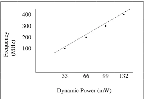
In The design is simulated for functional performance and power consumption. The power consumption analysis is performed using Xilinx XPower Tool. Fig 3 represents the graph of Dynamic Power variation of the proposed design with respect to the variation in the operational clock frequency on Kintex-7 device. The graph shows a linear variation in the dynamic power with respect to the clock frequency. Table II presents the comparison of the result from the work performed and the previous proposed design results. The comparison concludes an efficient reduction in the operational delay of the circuit performance in this work. The Power-Delay product proves the efficiency of the design realization on the configurable FPGA device of Xilinx from Kintex-7 Family. The FPGA that is used to perform simulation and synthesis of the present work is XC7K70T-2LFBG676. The simulation of the design is performed on Xilinx ISim Tool using VHDL Test-Bench. The RTL schematic block diagram of the proposed design is shown in Fig. 4. The result of functional simulation is shown in Fig 5.
400 •
Fre q u en cy (MH z)
300 •
200 •
100 •
33 66 99 132
Dynamic Power (mW)
Fig.3:Frequency Versus Dynamic Power variation of proposed design for Kintex-7 Family FPGA Device
Table I: Power-Delay Product Performance based Comparison of Proposed Design with Existing Designs Carry Select Adder Power (mW) Delay
(ns)
Power-Delay Product
64-bit Proposed Design 27 (100MHz) 16.032 433
81 (300MHz) 1299 134 (500MHz) 2148
64-bit Conventional CLA [10] 97 28.281 2743
64-bit CLA Proposed Design [10] 72 25.209 1821
16-bit CSLA ADP Efficient Design [18]
229 10.192 2334
An FPGA based Area-Delay Efficient 64-bit Carry Select Adder Design for High-Speed Applications
low power implementation hardware can be used for applications with a FPGA that has low internal voltage (Vint) and low auxiliary voltage (Vaux). The present design uses a combinational design for addition of 64-bit binary numbers. This design can be used with signal processing applications that require addition operation hardware. In future the multiplier and the test pattern generator can be configured to match the application specific requirement of the design for a BIST based hardware design implementation. The present work also has the scope of combining other existing hardware designs with this design for a complex logic implementation.
ACKNOWLEDGMENT
The authors thank Mr. Piyush Jain (Director, Innovative Technology Design and Training Center, Bhopal India) for sharing his ideas in-line with the presented work.
REFERENCES
[1]. Basant Kumar Mohanty and Sujit Kumar Patel, “Area Delay Power Efficient Carry Select Adder”, IEEE Transactions on Circuits and Systems-II, Volume-61 No.-6 June 2014.
[2]. Apoorva Singh and Soumitra Pande, “Literature Review on Carry Select Adder”, International Journal of Engineering, Management and Medical Research, Volume-1 Issue-7, July 2015.
[3]. Gurpreet Kaur, Loveleen Kaur and Navdeep Kaur, “Reduced Area Carry Select Adder with Low Power Consumptions”, International Journal of Emerging Engineering Research and Technology, Volume-3 Issue-3, March 2015.
[4]. M. D. Bobade and m. n. Kakatkar, “Implementation on FPGA Area-Delay Efficient Architecture of CSLA” International Journal of Advanced Research in Electrical, Electronics and Instrumentation Engineering, Volume-4 Issue-6, June 2015.
[5]. Lingappagari Raju and Tipparti Anil Kumar, “FPGA Implementation of Efficient Carry-Select-Adder using Verilog HDL”, International Journal and Magazine of Engineering, Technology, Management and Research, Volume-2 Issue-6, June 2015.
[6]. Korra Ravi Kumar, Santosh Kumar Allenki and G. Ramesh, “FPGA Implementation of Area Delay and Power Efficient Carry Select Adder Architecture Design”, International Journal on Recent and Innovation Trends in Computing and Communication, Volume-3 Issue-5, May 2015.
[7]. Theegala Ravinder Reddy and P. Anjaiah, “Design of High Speed Hybrid Carry Select Adder”, International Journal and Magazine of Engineering, Technology, Management and Research, Volume-2 Issue-7, July Volume-2015.
[8]. Priya H. Agrawal and Prashant R. Rothe, “Implementation of Area Delay and Power Efficient Carry Select Adder”, International Journal of Innovative Research in Electrical, Electronics, Instrumentation and Control Engineering, Volume-3 Issue-7, July 2015.
[9]. Priya H. Agrawal and Prashant R. Rothe, “Implementation of Fast Low-Power and Area Efficient Carry Select Adder”, International Journal on Recent and Innovation Trends in Computing and Communication, Volume-3 Issue-4, April 2015.
[10]. S. Banu Priya and G. Lingeswaran, “Area Delay Power Efficient and Implementation of Modified Square-Root Carry Select Adder Architecture”, International Journal for Trends in Engineering and Technology, Volume-4 Issue-2, April 2015.
[11]. Priya Meshram, Mithilesh Mahendra and Parag Jawarkar, “Designed Implementation of Modified Area Efficient Enhanced Square-Root Carry Select Adder”, International Journal for Research in Emerging Science and Technology, Volume-2 Issue-5, May 2015.
[12]. S. Murugeswari and S. Kaja Mohideen, “Design of optimized Low-Power and Area-Efficient Digital FIR Filter using Modified Group Structures based Square-Root Carry Select Adder”, Research Journal of Applied Sciences, Engineering and Technology, January 2015.
[13]. K. Bala Sindhuri, “Implementation of Regular Linear Carry Select Adder with Binary to Excess-1 Converter”, Unternational Journal of Engineering Research, Volume-4 Issue-7, July 2015.
[14]. Jasbir Kaur and Lalit Sood, “Design of Modified Carry Select Adder for Addition of more than Two Numbers”, International Journal of Engineering Research and General Science, Volume-3 Issue-3 Part-2, May-June 2015.
[15]. S. A. Mashankar, R. D. Kadam and P. R. Indurkar, “Power Efficient Carry Select Adder using D-Latch” International Research Journal of Engineering and Technology, Volume-2 Issue-3, June 2015. [16]. Anna Johnson and Rakesh S., “High Speed Non-Linear CSA used in Wallace Tree Multiplier and in
Radix-4 Booth Recorded Multiplier”, International Journal of Innovative Science, Engineering and Technology, Volume-2 Issue-3, March 2015.
[18]. Anupriya Chandran, “Design and Implementation of Reduced-Area and Low Power SQRT CSLA and its Applications in ALU”, International Journal of Innovative Research in Computer and Communication Engineering, Volume-3 Issue-9, September 2015.
[19]. Deepak Kumar Patel, Raksha Chouksey and Minal Saxena, “An Efficient VLSI Architecture for Carry Select Adder without Multiplexer”, International Journal of Computer Applications, Volume-127 No.-9, October 2015.
[20]. Madhurima Bose and Sourabh Sharma, “Implementation and Analysis of High-Speed and Area-Efficient 64-bit Carry Select Adder” International Journal of Engineering Science and Innovative Technology, Volume-4 Issue-4, July 2015.