Implementation of Low Power RISC Based
Flexible DSP Processor
Reena Ramadevi T¹ Raghavaiah B²
¹PG scholar, Dept of ECE, CEC, chirala, AP, India ²Associate Professor, Dept of ECE, CEC, Chirala, AP, India
Abstract
The computers that which uses simple algorithms for solving the problems such machines are called as the Reduced Instruction Set Computers. A processor must have the capability of performing arithmetic logical operations and the capability of transferring the data. The major blocks of the processor are Program counter (PC), Flexible computational unit (FCU), Control unit (CU), Accumulator, Instruction register (IR), Memory and additional logic.
RISC in fact enhances the performance of processor by taking into consideration the factors like simple architecture construction and instruction set, easy instruction set for decoding and simplified control architecture. With the use of Peres reversible logic gates in the proposed processor having RISC 32 bit wide architecture there may be size reduction when compare with the conventional architecture based on carry save logic adder approach. The RTL (Register transfer level) is designed based on VERILOG and the simulation and synthesis is performed by XILINX ISE 12.3i.
Key words
: RISC, Reversible logic gates, Carry save logic, XILINX.I.
INTRODUCTION:The processor design which is based on RISC architecture contains different design blocks like FCU, Accumulator, PC, IR, Memory, CU, and additional logic. The design incorporates some of the following issues which are based on 32 bit data and 28 bit address. It Uses rigid 32 bit wide instruction format , 4 bit wide op-code, capability of managing 15 instructions, has 256 memory locations, 32-bit registers (IR,ACC), also having of capability for implementing pipelining of 2-staged which is nothing but execute and fetch cycles overlapping with No
interrupts and No conditional branches, Data that it handles is unsigned integer type. The FCU performs both logical and arithmetic operations along with transfer set of instructions (shift right and shift left etc). It takes data and acc as inputs to generate output with the provided opcode. Based on the execlk only all the blocks are in sync with respect to its raising edge.
The FCU performs all arithmetic operations (addition, Subtraction, multiplication, and division) and logic operations. Buffer requirement is to make sure of achieving bi-directional operation. Multiplexer provides memory access to either IR (instruction register) or PC (program counter) based on Fetch signal. Memory block can handle instructions along with data operations. In order to access both data and instructions through a single address port a multiplexer is needed. Based on the fetch status it selects address. If the fetch signal is high pcout is selected and irout is selected when fetch signal is low.
The PC always point out the next instruction address. The FPU takes an instruction from memory by fetching, executes it and increments the content of PC. Instruction register is a 32-bit register which gets loaded with data from the memory. When LdIr signal is high, the bus contents of data has loaded into the IR. The 4-MSB’s of this loaded data [31:28] are the OpCode of the Instruction and the remaining bits [27:0] are the address of a memory location tofetch the subsequent data.
memory read, memory write. When LdAcc is set high, the output of the FCU is loaded into the accumulator. When Ldpc is set high the address is loaded by pc from where the subsequently instruction is to be fetched. When Ldir is set high the IR is loaded which has to be executed. If increment PC signal is set high, PC becomes PC plus one to the previous value .If write signal is set high and read low then the data bus is being written on the address of the memory location indicated by read signal is high and write low this is memory read operation and the data at the memory address indicated is placed on the data bus.
II. Flexible Processor architecture
Let us consider an instance when some information is stored in the memory. Now when the system is switched on, CPU is initialized. In order to fetch an instruction, as a result the program goes that is pointed out by the program counter memory. During the negative edge of the fetch signal, the output of the IR is selected, while the PC output is selected during the positive edge of fetch cycle
.
fig.1: Flexible processor architecture.
The FCU performs arithmetic (addition, subtraction etc) and/or logical operations (and,or etc). The operation at the instance is purely decides based on the selection lines. Using the VHDL Languagethe
modules are realized in the design
.
Fig.2: FCU block diagram.
In computing, FCU is a block which can performs both the operations of logical and the arithmetical. The FCU is a primary logic in the CPU whose purposes such as maintaining timers. The FCU accepts the inputs in terms of integers and will perform the corresponding operation and results the output. The FPU block plays a key role for getting the results which can convert one form of number to other format very easily using the used software XILINX. The proposed FCU unit performs addition, subtraction, multiplication, and, or, nand, nor along with shifting operations like right shift and left shift. The 32 bit size operations is developed using the VERILOG language. The performance of the total CPU is mainly depending upon the FPU unit.
The FPU results are based on the selection unit. Based on the selection line the corresponding operation is performed. The results of the FPU are taken by the accumulator and perform the corresponding operation.
III. Reversible Logic Gates
:
reversible gates symbols and their equations are given below.
Feynman Gate
Figure 3 shows a 2*2 Feynman
gate. Feynman gate is also called as Controlled NOT gate or CNOT gate. It is equivalent to single control input tofili gate.Fig.3: feynman gate and its symbolic
representation.
Toffoli Gate
Figure 4 shows a 3*3 Toffoli gate The input vector is I(A, B, C) and the output vector is O(P,Q,R). The outputs are defined by P=A, Q=B, R=A(B xor C). Quantum cost of a Toffoli gate is 5. It has two control inputs.
Fig.4: Toffoli gate and its symbolic
representation.
Peres Gate:
Figure 5 shows 3*3 Peres gate. The input vector is I (A,B,C) and the output vector is O (P,Q,R). the output is defined by P=A, Q= A^B and R= A&B ^C. quantum cost of a Peres is 4. It needs two Toffoli gates for its construction.
Fig.5: Peres gate and its symbolic
representation.
CNOT GATE
CNOT gate is also known as
controlled-not gate. It is a 2*2 reversible gate. The CNOT gate
can be described as:
Iv = (A, B) ; Ov = (P= A, Q= A B)
Iv and Ov are input and output vectors
respectively.m Quantum cost of CNOT gate is 1.
Figure shows a 2*2 CNOT gate and its symbol.
Fig.6: CNOT gate and its logic symbol.
NFT Gate:
It is a 3x3 gate and its logic circuit and its quantum
implementation is as shown in the figure. It has
quantum cost five
IV.
Results
RTL schematic:
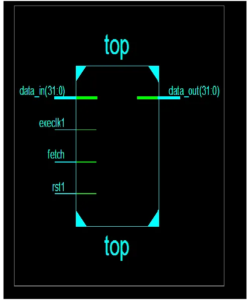
The RTL SCHEMATIC gives the information about the user view of the design. The inputs and outputs are mentioned in the left and right hand side of the block. The inputs are data_in, execlk1, fetch and rst1.The outputs are data_out.
Fig 8: RTL TOP Module
Internal architecture: The internal architecture
representation of the design is given below
.
Fig 9: RTL Schematic
Technological schematic: The technological
schematic gives the information about the chip view
Fig 10: Technology Schematic
WAVEFORM
Fig 11: Output wave form
The outputs are obtained based on the operational code which is provided. The operations which are performed are with 32 bit wide. The fetch and execlk1 signals are given as clock signal and for the remaining inputs the data has to be provided in the integer format. The buffer signal y1 has made enable to perform the operation without any interruption. The outputs are seen in the data_out signal and the inputs are provided with the signal data_in.
V.
Conclusion
RISC in fact improves the concert of processor having simple architecture for controlling and construction with the instruction set, easy for decoding. For proceeding with these operations, this processor contains the CU, FCU, PC, Accumulator, IR, Memory and additional logic. In the proposed design, the logic used is RCA with only 20.520w and occupies less area having 270 LUT's when compared with the existing carry save technique with a power consumption of 25.232 w and with area of 332 in terms of LUT's . The RTL (Register transfer level) is designed based on VERILOG and the simulation, synthesis was performed by XILINX ISE 12.3i.
R
EFERENCES:
[1] P. Ienne and R. Leupers, Customizable Embedded Processors: Design Technologies and Applications. San Francisco, CA, USA: Morgan Kaufmann, 2007.
[2] P. M. Heysters, G. J. M. Smit, and E. Molenkamp, “A flexible and energy-efficient coarse-grained reconfigurable architecture for mobile systems,” J. Supercomput., vol. 26, no. 3, pp. 283–308, 2003.
[4] M. D. Galanis, G. Theodoridis, S. Tragoudas, and C. E. Goutis, “A high-performance data path for synthesizing DSP kernels,”
IEEE Trans. Comput.-Aided Design Integr. Circuits Syst., vol. 25, no. 6, pp. 1154–1162, Jun. 2006.
[5] K. Compton and S. Hauck, “Automatic design of reconfigurable domainspecific flexible cores,” IEEE Trans. Very Large Scale Integr. (VLSI) Syst., vol. 16, no. 5, pp. 493–503, May 2008.
[6] S. Xydis, G. Economakos, and K. Pekmestzi, “Designing coarse-grain reconfigurable architectures by inlining flexibility into custom arithmetic data-paths,” Integr., VLSI J., vol. 42, no. 4, pp. 486–503, Sep. 2009.
[7] S. Xydis, G. Economakos, D. Soudris, and K. Pekmestzi, “High performance and area efficient flexible DSP datapath synthesis,”