Implementation of DSP Based Sinusoidal Pulse
Width Modulation for Three Thase Inverter
Krupa M Assistant Professor
Department of Electrical and Electronics
GSSS Institute of Engineering and Technology for Women, Mysuru
Abstract
This paper presents the implementation of sinusoidal pulse width modulation for a three phase Bridge inverter. Basically three sinusoidal reference signals which are phase shifted by120 degree apart from each other and compliment of these three sinusoidal signals are compared with the carrier signal to generate six different PWM signals for six switches of three phase inverter.LC filter is employed to reduce higher order harmonics in the three phase inverter output voltage. Closed loop operation is carried out. Hardware is implemented for open loop system where the SPWM algorithm is implemented in DSPIC30F2010. The efficiency of the inverter is high and offers less harmonic distortion. The proposed technique is simulated using MATLAB-Simulink model and THD is measured.
Keywords: Sinusoidal Pulse Width Modulation, Total Harmonic Distortion, DSPIC30F2010
________________________________________________________________________________________________________
I.
INTRODUCTION
Sinusoidal pulse width modulation technique is applied to three phase inverter to obtain necessary output sinusoidal voltage without much harmonics. This is possible if the sampling frequency is much higher than the fundamental output frequency of the inverter. This method is characterized by constant amplitude pulses with various duty cycles in each period [1]. Most popular application of sinusoidal pulse width modulation is the motor control and inverters.
This paper presents the implementation of sinusoidal pulse width modulation for three phase inverter to obtain output voltage with reduced harmonics. Output of the inverter is filtered using a second order passive filter in order to obtain a sine wave output [2]. Total harmonic distortion of the output voltage of the inverter with filter and without filter are measured.THD of the output voltage of inverter with filter is less compared to the THD of the output voltage of inverter without filter. Closed loop operation is carried out using PI controller to obtain constant inverter output.
II.
THREE PHASE SPWM INVERTER
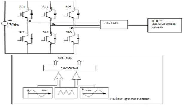
Basic block diagram of SPWM implemented three phase inverter is shown in figure 1. It can be divided into two parts. Power circuit and control circuit. Power circuit includes three phase inverter, DC supply, star connected load and LC filter. Control part includes PI controller and a sensing circuit. Power circuit includes semiconductor devices which have non linear characteristics. This non linearity will generate dominant harmonics in the inverter output. Hence LC filter is employed to filter major harmonics from the inverter output. Trigger pulses for the inverter is generated using sinusoidal pulse width modulation technique.
III.
SPWM GENERATION
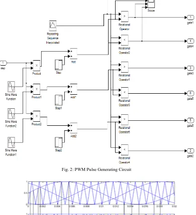
Six PWM pulses are generated for six switches of three phase inverter. The pulses for lower switches are compliment to that of upper switches of respective legs. Three sinusoidal reference signals which are phase shifted by 120 degree and these signals are compared with a triangular carrier wave [1]-[2]. Thus three pulses with constant amplitude and with different duty cycle for each period is obtained. These three pulses are used to trigger the upper switches of the bridge inverter. Then the compliment of these three pulses is obtained and is used to trigger the three lower switches of the bridge inverter. The pulse generating circuit is as shown in Figure. 2. Figure. 3 shows the comparison of triangular and three phase sine wave and the generated PWM for upper and lower switch of first leg.
Fig. 2: PWM Pulse Generating Circuit
IV.
SIMULATION RESULT AND DISCUSSION
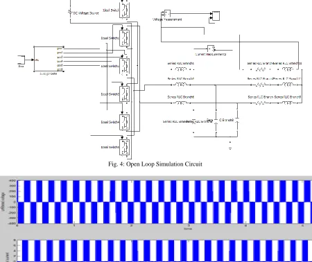
In an open loop operation, three phase inverter output is given to star connected R load without any output filter circuit. Since there is no output filter, because of non linear characteristics of inverter switches, output voltage and current waveforms of inverter will have dominant harmonics. Open loop simulation circuit is as shown in figure 4. With the input DC voltage of 400V, the output voltage and current waveforms of inverter is as shown in figure. 5.
Fig. 4: Open Loop Simulation Circuit
Fig. 5: Output Voltage and Current without Filter
Fig. 6: 3-Ø Output Voltage and Current with Filter
THD and harmonic contents of output voltage is measured for the inverter with filter and without filter in the open loop operation. THD of the inverter without filter is 54.10% where as THD of inverter with filter is 0.22%. The harmonic contents which are present in the output voltage of the inverter with filter and without filter are as shown in figure 7 and figure 8. It is observed that the higher harmonic content in the output voltage of the inverter with filter is reduced compared to output voltage of the inverter without filter.
Fig. 8: FFT Analysis of Output Voltage of Inverter with Filter
In an open loop operation, output voltage varies whenever there is variation in the input voltage. This may affect the load characteristics. Hence closed loop operation of three phase SPWM inverter is carried out using PI controller. The closed loop simulation circuit is as shown in figure. 9.
In the closed loop operation, the output voltage is fed back and compared with the reference voltage, obtained error signal is fed to the controller. PI Controller modifies the duty cycle of PWM to obtain the desired output. Because of the controller action, the output voltage remains constant whenever there is a variation in the input voltage and hence the load characteristics remain unaffected [4]. Since input reference voltage is DC and the output voltage which has to be compared with reference voltage is AC, comparison is not possible. So for this reason, the output voltage has to be converted to DC using rectification process. A full bridge rectifier circuit is used for rectifying the output voltage. Since the rectified output is very much higher than the reference voltage, the rectified output voltage has to be reduced so as to match the reference voltage. This is done using a voltage divider circuit. A capacitor filter is employed in order to obtain constant DC from a pulsating rectified output. Then the rectified and filtered output signal is compared with reference signal and error signal is given to PI controller. The simulation for rectifier and voltage divider circuit is as shown in figure 10 and filtered rectifier output is shown in figure 11. The values of Kp and Ki of the PI controller are designed such that the error signal should be zero and the load voltage should remain constant with variation in the input voltage [4]. Design parameters for entire circuit are given in table 1.
Figure.12 shows the reference voltage, rectified feedback voltage and the error signal.
Fig. 10: Rectifier and Voltage Divider Circuit for Rectifying and Reducing the Output Voltage
Fig. 11: Filtered Rectifier Output
Table - 1 Design Parameters parameters Values Input DC voltage 400V Required output voltage 200V r m s Fundamental frequency 50Hz
Switching frequency 1kHz filter inductor L 30mH Filter Capacitor C 150uF Kp, Ki 2, 10 Capacitor filter 200uF Voltage divider R1 198.58KΩ Voltage divider R2 1.41 KΩ
V.
HARDWARE IMPLEMENTATION
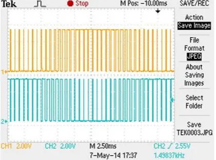
Open loop system of the proposed technique is implemented in hardware with no load condition. A DSPIC30F2010 is used to implement the SPWM algorithm. To generate a sine wave, 64 points sine table is generated. The switching frequency is set as 1.5 kHz. Different duty cycles are set to all three legs of the bridge inverter. Figure 13 shows the SPWM pulses generated for leg 1 where the two pulses are compliment to each other. The dead time between the switching of upper and lower switch is set as 21usec. Dead time of 20usec is achieved as shown in figure 14. The unfiltered inverter output voltage for phase a and phase b is as shown in figure 15 where the two waveforms are phase shifted by 1200 from each other. The experimental setup is as shown is figure 16.
Fig. 14: Dead Time Between the Switching of S1 and S2 Switches
Fig. 15: Unfiltered Output Voltage of the Inverter (Phase A, Phase B Which Are Phase Shifted by 1200)
VI.
CONCLUSION
This paper implements the SPWM for three phase inverter. Six different pulses are generated to trigger the switches of bridge inverter. Second order LC filter is used across inverter output to reduce the harmonic distortion in the inverter output voltage. Closed loop simulation is carried out to obtain constant inverter output. THD is measured and is observed to be 0.22% for inverter with filter which is less than that of the inverter without filter and also higher order harmonics are reduced. Proposed system is analyzed using MATLAB simulations. Open loop system is implemented in hardware using DSPIC30F2010. SPWM pulses are generated and unfiltered ac output voltage is obtained.
REFERENCES
[1] M. F. N. Tajuddin, N. H. Ghazali, I. Daut and B. Ismail “Implementation of DSP Based SPWM for single phase inverter” SPPEDAM 2010 International
Symposium on Power Electronics.
[2] Mohan, Undeland, Riobbins “Power Electronics”, converters, application and design.
[3] Bunyamin Tamyurek, Member. IEEE “A high performance SPWM controller for three phase UPS systems operating under highly nonlinear loads” IEEE
transactions on power electronics, vol. 28, no. 8, august 2013.