Modeling and Simulation Of Transformer-less Grid Connected Photovoltaic
System With Artificial Neural Network Based Power Converter
Gouthami Dixith A M. Tech. Scholar, Dept of EEE
Balaji institute of Technology and Sciences, JNTUH, Warangal, Telangana, India
Madhuri G
Asst. professor, Dept of EEE
Balaji institute of Technology and Sciences, JNTUH, Warangal, Telangana, India
Abstract:- This paper describes a novel transformer less grid connected ANN based power converter with negative grounding for a photovoltaic generation system. The negative terminal of the solar cell array can be directly connected to the ground in the proposed grid-connected power converter to avoid the transparent conducting oxide corrosion that occurs in some types of thin-film solar cell array. The proposed grid-connected power converter consists of a dc–dc power converter and a dc–ac inverter. The salient features of the proposed power converter are that some power electronic switches are simultaneously used in both the dc–dc power converter and dc–ac inverter, and only two power electronic switches operate at high switching frequency at the same time (one is in the dc– dc power converter and the other is in the dc–ac inverter). The leakage current of the photovoltaic generation system is reduced because the negative terminal of the solar cell array is connected directly to the ground. Finally, a prototype was developed to verify the performance of the proposed grid- connected power converter. Performance of the proposed ANN based grid-connected power converter is verified using MATLAB/SIMULINK.
I. INTRODUCTION
The use of fossil fuels has resulted in the emission of greenhouse gases and the cost of fossil-fuel energy has become higher and higher. Climate change, caused by these greenhouse gases, has seriously damaged the environment. Because of the problems associated with climate change, interest in renewable energy sources, such as solar power and wind power, has increased [1]–[12]. Many materials can be used to manufacture solar cells, but polycrystalline Si and mono crystalline Si are the most widely used. A thin-film solar cell can generate power under conditions of low irradiation.
Therefore, the thin-film solar cell has the potential to generate electrical power for a longer time than a crystalline Si solar cell. Since the
thin-film cell can be easily combined with glass, plastic, and metal, it can be incorporated in green architecture. The use of thin-film solar cells has increased steadily and this trend is set to continue in the future. In general, an earth parasitic capacitance will be generated between solar modules and their ground. This parasitic capacitance is about 50–150 nF/kW for a glass- faced solar cell array [4], [13].
Fig. 1. Basic configurations of grid-connected photovoltaic generation system with an isolation transformer.(a) Line frequency transformer.(b)
High-frequency transformer.
However, this capacitance is increased to 1
International Journal of Science Engineering and Advance Technology,
IJSEAT, Vol 3, Issue 6
ISSN 2321-6905
JUNE-2015
www.ijseat.com
Page 234
Consequently, the life of thin- film solar modules is shortened However, TCO corrosion can be prevented by the negative grounding of solar modules. Using an isolation transformer in the grid-connected inverter can solve the problem of the leakage current caused by the earth parasitic capacitance in solar modules. There are two types of grid-connected inverter with an isolation transformer. One is a line frequency transformer, and the other is a high-frequency transformer.
Fig. 1(a) shows a grid connected photovoltaic generation system with a line frequency transformer. The solar modules can be grounded directly and there is no current path for leakage current because the line frequency transformer is isolated [4], [19]. This system supplies no dc current to the grid and has the advantage of a simple control circuit. However, the line frequency transformer’s
disadvantages are large volume, high weight, and high cost. Fig. 1(b) shows a grid-connected photovoltaic generation system with a high frequency transformer.
The transformer is incorporated in a dc–dc converter and is operated at high frequency to reduce volume and cost. However, the control circuit of this grid-connected photovoltaic generation system is complicated due to the use of a transformer-isolated dc–dc converter. Besides, the high-frequency transformer is not placed at the output of the grid-connected photovoltaic generation system, so it cannot prevent the dc current from injecting the grid. The use of an isolation transformer in the grid-connected photovoltaic generation system should be avoided due to cost, size, and efficiency. In general, the bridge-type dc–ac inverter is used in the grid-connected photovoltaic generation system [15]. However, a conventional bridge- type dc–ac inverter, without an isolation transformer, results in the problem of leakage current because it cannot sustain the voltage of its negative terminal at a constant value. Recently, many dc–ac inverter topologies have been proposed to solve the problem of leakage current [7].
This paper proposes a transformer less grid-connected ANN integrated power converter with negative grounding for a photovoltaic generation system. The proposed transformer less grid-connected power converter simultaneously solves the problems of leakage current and negative grounding as the topologies shown in [7] and [18]. The negative grounding of the solar cell array in the proposed paper is achieved by a boost dc–dc converter and select switches. Therefore, the problem of TCO corrosion in Cd-Te or A-Si thin-film solar
modules is also solved. Finally, a prototype was developed and tested to verify the performance of the proposed transformer less photovoltaic generation system.
II. LEAKAGE CURRENT OF HALF-BRIDGE INVERTER
Fig. 2 shows the relevant circuit configurations. In the following analysis, the capacity of the solar cell array shown in Fig. 2 is assumed to be 1kW. This section analyzes and discusses the problem of leakage current in a grid-connected photovoltaic generation system that uses a conventional half-bridge inverter, a conventional full bridge inverter, and a diode-clamped multilevel half-bridge inverter. An equivalent capacitor Cp is serially connected to an equivalent resistor Rg 1 to represent the parasitic elements of the solar cell array, and these are connected between the negative terminal of the solar cell array and the ground.
The utility is connected to the ground by an equivalent resistor Rg2. The capacitance of the
parasitic capacitor Cp is typically 1 μF in a 1-kW solar cell array. Since the utility voltage is 120 V, Rg2 must be lower than 25 Ω to satisfy the
requirements Fig. 2(a) shows a conventional half-bridge inverter, which is controlled by pulse width modulation (PWM) and named as type 1. Fig. 2(b) shows a conventional full-bridge inverter. The conventional full-bridge inverter can be controlled by a bipolar PWM or a unipolar PWM, named as type 2 and type 3, respectively.
Fig. 2(c) shows the diode-clamped multilevel half-bridge inverter named as type 4. A filter inductor Lf connected to the output of the dc–ac inverter is used for filtering the switching harmonic of the dc–ac inverter. Table I shows the main parameters of the simulation system. Fig. 3 shows
the simulation results for the resistors Rg 1 = 1 Ω and Rg 2 = 1 Ω. As can be seen, the grounding voltage vg
and the leakage current ig differ for different types of dc–ac inverters. For the conventional half- bridge and diode-clamped multilevel half-bridge inverters (type 1 and type 4) the neutral line of the utility is directly connected to the middle point of the split dc capacitors. The voltage between the negative terminal of the solar cell array and the ground is stabilized by the lower dc capacitor of these types of dc–ac inverters.
TABLE I
As seen in Fig. 3, the voltage of the negative terminal for these types of dc–ac inverters is−200 V.
A voltage ripple with a frequency equaling that of the utility is incorporated in the voltage of the negative terminal because the ac current connected to the utility passes through the split dc capacitors. This voltage ripple is very small and depends on the capacitance of the split dc capacitors. Since the impedance of the earth parasitic capacitance is very large at the utility frequency, the leakage current of the utility frequency is very small. Fig. 3 shows a small high-frequency leakage current in the half-bridge inverter. This is due to the equivalent ground resistor Rg 2 of the utility and switching operation of the power electronic switches. However, the leakage current for the half-bridge inverter is less than 2.5 mA.
Fig. 2. Inverter topologies used in the grid-connected photovoltaic generation system. (a) Conventional half-bridge inverter. (b) Conventional full-bridge inverter. (c) Diode-clamped multilevel half-bridge
inverter.
During the positive half-cycle of the utility voltage, the switching operation occurs at the upper side of the diode clamped multilevel half-bridge inverter and results in a switching ripple in the upper side capacitor. However, the voltage of the lower side capacitor is sustained and no leakage current is generated between the negative terminal and the ground. Similarly, this switching ripple will appear in the lower side capacitor during the negative half-cycle of the utility voltage and result in a small leakage current between the negative terminal and the ground. However, the leakage current for the diode-clamped multilevel half-bridge inverter is still less than 2 mA.
International Journal of Science Engineering and Advance Technology,
IJSEAT, Vol 3, Issue 6
ISSN 2321-6905
JUNE-2015
www.ijseat.com
Page 236
offset are 90 V, 60 Hz, and −100 V,
respectively. The voltage at the negative terminal of type 2 contains no pulsating voltage at the switching frequency due to the symmetric switching of the bipolar PWM. Since this voltage ripple is low frequency, the peak value of the leakage current is smaller than 50 mA. However, this leakage current is larger than that of the conventional half bridge and the diode-clamped multilevel half-bridge inverters.
Fig. 3. Simulation results for different types of
inverter under 1 μF, Rg 1 =1 Ω, and Rg 2 = 1 Ω.
Fig. 3 also shows that the voltage at the negative terminal of type 3 contains a pulsating voltage with a frequency equaling the switching frequency due to the asymmetric switching of the uni polar PWM. The magnitude of this pulsating voltage is 90 V and results in a serious leakage current (about 1A) through the parasitic capacitance of the solar cell array. Fig. 4 shows the simulation results for resistors
Rg 1 = 10 Ω and Rg 2 =10Ω.As can be seen, the
simulation results are similar to those of Fig. 3. From the simulation results shown in Figs. 3 and 4, it can be seen that the leakage current in the conventional full-bridge inverter controlled by the unipolar PWM
is too large to comply with the standard VDE 0126-1-1 [25].
The major reason for grounding connection is safety. In practical applications, the grounding resistance is usually very small. The earth parasitic capacitance, between the solar cell array and the ground, will cause leakage current and result in additional power loss.
Fig. 4. Simulation results for different types of inverter under 1μF, Rg 1 = 10Ω, and Rg 2 = 10Ω.
Table II shows the calculated power loss caused by the leakage current for the same earth
parasitic capacitance (1 μF) and different resistors Rg 1 and Rg 2 (1 Ω, 5 Ω, and 10 Ω) in a 1-kW solar cell array [10], [26]. The power loss is the product of the square of the leakage current and the summation of equivalent resistors Rg 1 and Rg 2 . As can be seen in Table II, the leakage currents are small in the conventional half-bridge inverter, the conventional full-bridge inverter with bipolar PWM, and the diode-clamped multilevel half-bridge inverter. As seen in Table II, the power loss caused by the leakage current in types 1, 2, and 4 is very small. However, the power loss caused by the leakage current is
International Journal of Science Engineering and Advance Technology,
IJSEAT, Vol 3, Issue 6
ISSN 2321-6905
JUNE-2015
www.ijseat.com
Page 236
offset are 90 V, 60 Hz, and −100 V,
respectively. The voltage at the negative terminal of type 2 contains no pulsating voltage at the switching frequency due to the symmetric switching of the bipolar PWM. Since this voltage ripple is low frequency, the peak value of the leakage current is smaller than 50 mA. However, this leakage current is larger than that of the conventional half bridge and the diode-clamped multilevel half-bridge inverters.
Fig. 3. Simulation results for different types of
inverter under 1 μF, Rg 1 =1 Ω, and Rg 2 = 1 Ω.
Fig. 3 also shows that the voltage at the negative terminal of type 3 contains a pulsating voltage with a frequency equaling the switching frequency due to the asymmetric switching of the uni polar PWM. The magnitude of this pulsating voltage is 90 V and results in a serious leakage current (about 1A) through the parasitic capacitance of the solar cell array. Fig. 4 shows the simulation results for resistors
Rg 1 = 10 Ω and Rg 2 =10Ω.As can be seen, the
simulation results are similar to those of Fig. 3. From the simulation results shown in Figs. 3 and 4, it can be seen that the leakage current in the conventional full-bridge inverter controlled by the unipolar PWM
is too large to comply with the standard VDE 0126-1-1 [25].
The major reason for grounding connection is safety. In practical applications, the grounding resistance is usually very small. The earth parasitic capacitance, between the solar cell array and the ground, will cause leakage current and result in additional power loss.
Fig. 4. Simulation results for different types of inverter under 1μF, Rg 1 = 10Ω, and Rg 2 = 10Ω.
Table II shows the calculated power loss caused by the leakage current for the same earth
significant in type 3, and it will evidently degrade the system efficiency. Besides, it can also be found that the calculated power loss of type 3 increases as the resistance is increased. Additionally, the leakage current will cause additional power loss at the filter inductor and power electronic switches. The power loss caused by the leakage current of type 3 will be higher than 1% in practice after considering the effects of both the parasitic and nonparasitic components.
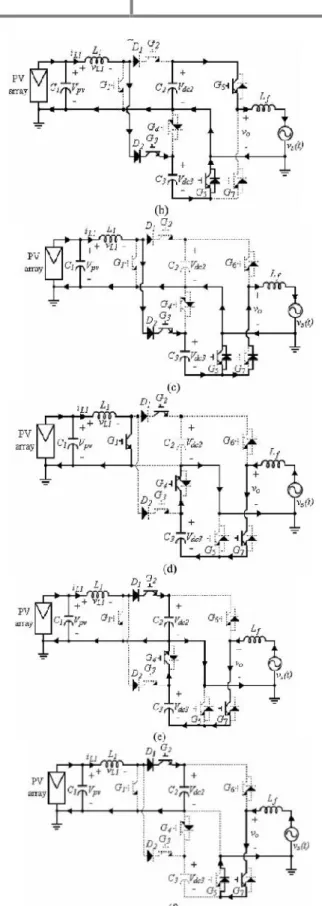
III. CIRCUIT ANALYSIS
Fig. 5 shows the circuit configuration of the proposed photovoltaic generation system. As can be seen, the grid- connected power converter is
transformer less, and its negative terminal is connected directly to the ground. Both the problems of TCO corrosion and leakage current in C d- Te or A-Si thin-film solar cell array can be avoided. The proposed transformer less grid-connected power converter is composed of a dc–dc power converter and a dc–ac inverter. The dc–dc power converter is a boost converter. The dc–dc power converter consists of three dc capacitors C1, C2, and C3, an inductor L1 , two diodes D1 and D2 , and four power electronic switches G1 , G2 , G3 , and G5 . The dc–dc power converter converts the dc voltage of the solar cell array to a stabilized dc voltage.
TABLE II
CALCULATED POWER LOSS CAUSED BY THE LEAKAGE CURRENT UNDER DIFFERENT R g 1 AND R g 2 IN 1-KWTHIN-FILM SOLAR MODULES
Fig. 5. Circuit configuration of the proposed transformerless negative grounding photovoltaic generation system.
The dc–ac inverter consists of two dc capacitors C2 and C3, an ac inductor Lf, and four power electronic switches G4, G5 , G6 , and G7 . The dc–ac inverter further converts the output dc voltage
of the dc–dc power converter into ac power and injects into the grid. As seen in Fig. 5, the power electronic switch G5 controls both the dc–dc power converter and the dc–ac inverter.
International Journal of Science Engineering and Advance Technology,
IJSEAT, Vol 3, Issue 6
ISSN 2321-6905
JUNE-2015
www.ijseat.com
Page 238
Fig. 6. Switching pattern for the power electronic switches of the proposed Transformer less negative grounding photovoltaic generation system. (G2 , G7 ), (G3 , G5 ): low frequency. G1 , G4, and G6 : high
frequency.
Fig. 6 shows the switching pattern for the power electronic switches of the proposed transformer less grid-connected power converter. As can be seen, (G2 , G7 ) and (G3 , G5 ) are switched in opposition and synchronous with the utility voltage, respectively. G1 is switched at high frequency to store or release the energy in the inductor L1 , and then regulate the output voltage of the dc–dc power converter. G6 and G4 are, respectively, switched at high frequency during the positive half-cycle and the negative half-cycle of the utility voltage to control the output current of the dc–ac inverter. Since only one power electronic switch in the dc–ac inverter is switched at high frequency, the power loss caused by the switching operation is reduced.
Fig. 7 shows the timing sequence for power electronic switches of the proposed power converter. Fig. 7(a) is the timing sequence for power electronic switches during the positive half-cycle of the utility voltage. During the positive half cycle of the utility voltage, the dc–dc power converter charges capacitor C3 so the duty cycle (Du 3 = ton3/T2) of G1 controls the voltage of capacitor C3 . The capacitor C2 supplies power to the dc–ac inverter, and G6 of the dc-ac inverter is switched at high frequency to control the output current.
Fig. 7. Timing sequence for power electronic switches of the proposed power converter. (a) Positive half-cycle. G2 , G3, G4 , G5, and G7 : low frequency, G1 and G6 : high frequency. (b) Negative half-cycle. G2 , G3 , G5 , G6 and G7 : low frequency,
G1 , G4 : high frequency.
As seen in Fig. 7(a), the operation of power electronic switches during the positive half-cycle can be divided into three time intervals. The current paths, during these time intervals, are shown in Fig. 8 and described as
1) [t01, t02]
to G3 to prevent C3 from short circuit. In the dc–ac inverter, G6 is switched ON and the output voltage vo is+Vdc2. The output current of the dc–ac inverter is supplied from C2.
2) [t02, t03]
The current path during this time interval is shown in Fig. 8(b). In the dc–dc power converter, G1 and G2 are switched OFF. G3 and G5 are still ON. The energy stored in the inductor L1 is deenergized via the path D2 , G3 and the flying diode of G5 to charge the capacitor C3 . G6 of the dc– ac inverter is still ON, and the output voltage vo is still +Vdc2. The filter inductor of the dc–ac inverter is energized from C2 .
3) [t03, t04]
The current path during this time interval is shown in Fig. 8(c). In the dc–dc power converter, the energy stored in the inductor L1 is still deenergized via the path D2 , G3 and the flying diode of G5 to charge the capacitor C3 . G6 of the dc–ac inverter is switched OFF, and the output current is flowing through G5 and the flying diode of G7 to form a loop. Therefore, the voltage vo is 0, and the filter inductor of the dc–
ac inverter is reenergized.
Fig. 7(b) shows the timing sequence for power electronic switches during the negative cycle of the utility voltage. For the negative half-cycle of the utility voltage, the dc–dc power converter charges the capacitor C2 , so the duty cycle (Du 2 = ton2/T2) ofG1 controls the voltage of capacitor C2 . Capacitor C3 supplies power to the dc–ac inverter, andG4 of the dc–ac inverter is switched at high frequency to control the output current. As seen in Fig. 7(b), the operation of power electronic switches during the negative half-cycle of the utility voltage can also be divided into three time intervals.
Fig. 8. Current path under different time duration. (a) [t01 , t02 ]. (b) [t02 , t03 ]. (c) [t03 , t04 ]. (d) [t11 ,
International Journal of Science Engineering and Advance Technology,
IJSEAT, Vol 3, Issue 6
ISSN 2321-6905
JUNE-2015
www.ijseat.com
Page 240
The current paths during these time intervals of the negative half-cycle of the utility voltage are shown in Fig. 8(d)–(f). Because the operation of the negative half-cycle of the utility voltage is similar to that of the positive half-cycle, its explanation is superfluous.
V. ARTIFICIAL NEURAL NETWORKS (ANN)
The rapid detection of the disturbance signal with high accuracy, fast processing of the reference signal, and high dynamic response of the controller are the prime requirements for desired compensation in case of converters. The conventional controller fails to perform satisfactorily under parameter variations nonlinearity load disturbance, etc. A recent study shows that NN-based controllers provide fast dynamic response while maintaining stability of the converter system over wide operating range [10][12][13]. The ANN is made up of interconnecting artificial neurons. It is essentially a cluster of suitably interconnected nonlinear elements of very simple form that possess the ability to learn and adapt. It resembles the brain in two aspects: 1) the knowledge is acquired by the network through the learning process and 2) interneuron connection strengths are used to store the knowledge [14]-[15][16]. These networks are characterized by their topology, the way in which they communicate with their environment, the manner in which they are trained, and their ability to process information. ANN has gain a lot of interest over the last few years as a powerful technique to solve many real world problems.
Compared to conventional programming, they own the capability of solving problems that do not have algorithmic solution and are therefore found suitable to tackle problems that people are good to solve such as pattern recognition. ANNs are being used to solve AI problems without necessarily creating a model of a real dynamic system. For improving the performance of a UPQC, a multilayer feed forward- type ANN-based controller is designed. This network is designed with three layers, the input layer with 2, the hidden layer with 21, and the output layer with 1 neuron, respectively [18].
Structure of ANN:
Neural networks are models of biological neural structures. The starting point for most neural networks is a model neuron, as in Figure 9. This neuron consists of multiple inputs and a single output. Each input is modified by a weight, which
multiplies with the input value. The neuron will combine these weighted inputs and, with reference to a threshold value and activation function, use these to determine its output. This behavior follows closely our understanding of how real neurons work.
Fig.9. Model of neural
While there is a fair understanding of how an individual neuron works, there is still a great deal of research and mostly conjecture regarding the way neurons organize themselves and the mechanisms used by arrays of neurons to adapt their behavior to external stimuli. There are a large number of experimental neural network structures currently in use reflecting this state of continuing research. In our case, we will only describe the structure, mathematics and behavior of that structure known as the back propagation network. This is the most prevalent and generalized neural network currently in use.
Fig.10. Back propagation Network
Generally, the input layer is considered a distributor of the signals from the external world. Hidden layers are considered to be categorizers or feature detectors of such signals. The output layer is considered a collector of the features detected and producer of the response. While this view of the neural network may be helpful in conceptualizing the functions of the layers, you should not take this model too literally as the functions described may not be so specific or localized.
VI. CONTROL SYSTEM
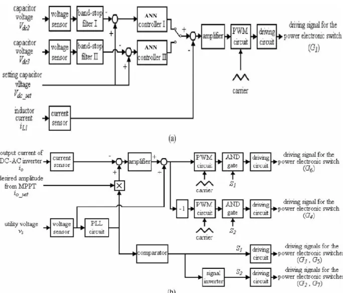
Fig. 11 shows the control block diagram for the proposed transformer less grid-connected ANN power converter. Fig. 11(a) is the control block diagram for the dc–dc power converter. G1 of the dc–
dc power converter controls the dc voltages of C2 and C3. As already mentioned, the positive and the negative half-cycles of the ac current are alternately supplied from the dc capacitors C2 and C3 , and the dc capacitors C2 and C3 are individually charged during different half-cycles. Therefore, the dc voltages of C2 and C3 will contain a voltage ripple with a frequency equaling the utility frequency.
The generating power of the solar cell array will decrease if their output voltage contains a voltage ripple. To avoid the voltage ripple delivered from the dc capacitors C2 and C3 to the solar cell array, the current in the inductor L1 must be ripple free. Consequently, the dc–dc power converter is Controlled by an outer voltage loop and an inner current loop. As mentioned previously,C2 andC3 are, respectively, charged by the dc–dc power converter in the negative and the positive half-cycles of the utility.
As seen in Fig. 11(a), the capacitor voltages Vdc2 and Vdc3 are detected and sent to band-stop filters I and II, respectively. The band-stop filters I and II are used to eliminate the utility frequency
ripple. The outputs of the band-stop filters I and II are subtracted from a setting capacitor voltage Vdc set, and then the results are sent to the of the switch is a reference current signal. Since the capacitor voltages Vdc2 and Vdc3 are controlled by the individual half cycle and individual ANN controller, the voltages of C2 and C3 can be balanced. The reference current signal and the detected inductor current are sent to a sub tractor, and then the result is sent to an amplifier.
The output of the amplifier is sent to a PWM circuit, and the output of the PWM circuit is sent to a driving circuit to generate the driving signal for G1 . Fig. 11(b) shows the control block diagram for the dc–ac inverter. The utility voltage is detected and fed to a phase-locked loop (PLL) circuit to generate a unity sinusoidal signal in phase with the utility voltage.
This unity sinusoidal signal is sent to a comparator to generate a square wave S1 whose phase is the same as the utility. The output signal of the comparator is sent to a driving circuit to generate the driving signals for G3 and G5. The output signal of the comparator is also sent to signal inverter. The output signal S2 of the signal inverter, which is out of phase with the utility voltage, is sent to a driving circuit to generate the driving signals for G2 and G7. The maximum power point tracking (MPPT) method used in this paper is modified from that used in a small wind-power generation system [27]. The function of MPPT can be obtained by perturbing the amplitude of the output current of the dc– ac inverter, and then observing the voltage variation of the solar cell array to determine the next perturbation direction for the amplitude of the output current of the dc–ac inverter.
The output of the MPPT control block is an amplitude signal. The outputs of the PLL circuit and the MPPT control block are sent to a multiplier to provide a reference output current for the dc–ac inverter. The reference output current and the detected output current of a dc–ac inverter are sent to a subtractor, and the result is then sent to an amplifier. The output of the amplifier and the detected utility voltage is sent to an adder. To avoid interference from the utility\ voltage, a feed forward control is used, and it is obtained by adding the detected utility voltage. The output of the accumulator is sent to a PWM circuit.
International Journal of Science Engineering and Advance Technology,
IJSEAT, Vol 3, Issue 6
ISSN 2321-6905
JUNE-2015
www.ijseat.com
Page 242
voltage. The output of the amplifier is also sent to an inverting amplifier. The output of this inverting amplifier is sent to a PWM circuit. The output of the PWM circuit and the signal S2 are sent to an AND gate, and then sent to a driving circuit to generate a driving signal for G4. This means G4 is operated at a high switching frequency during the negative half-cycle of utility Voltage. Note, only one power electronic switch in the dc–ac Inverter is operated at a high switching frequency.
The model of the dc–ac inverter with the current mode control is shown in Fig. 12, where kif is the gain of the current detector. As seen in Fig. 12, the feed forward control of the utility is also incorporated into the controller, and the gain of the feed forward control is 1/kpwm. Therefore, the interference of the utility voltage can be avoided by the feed forward control. The current controller is an amplifier with gain kc .
Fig. 12. Simplified model of the dc–ac inverter
VII. SIMULATION RESULTS
To verify the performance of the proposed converter is designed by using MATLAB/ SIMULINK. The power electronic switches G1–G7 used in this paper are insulated gate bipolar transistor modules, and the power diodes. The controllers of the dc–dc power converter and the dc–ac inverter are implemented in a MATLAB. The major parameters of the prototype are listed in Table III.
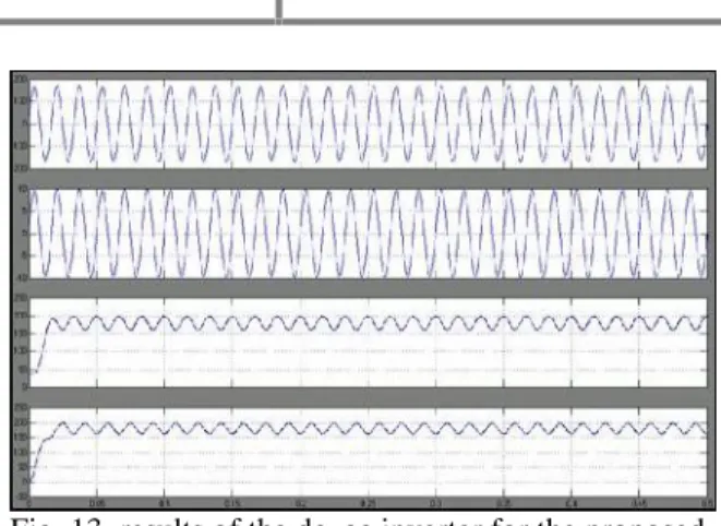
Fig. 13 shows the simulation results for the dc–ac inverter of the proposed transformerless grid-connected power converter under the steady state. The output power of the solar cell array is about 931 W. Fig. 13(b) shows that the output current of the dc–
ac inverter is sinusoidal and in phase with the utility voltage. The total harmonic distortions (THDs) of the utility voltage and the output current of the dc–ac inverter are less compare with conventional system.
TABLE III
MAJOR PARAMETERS OF THE PROTOTYPE
This verifies that the proposed transformerless grid-connected power converter can convert solar power to ac power with unity power factor. As seen in Fig. 13(c) and (d), both capacitor voltages Vdc2 and Vdc3 remain stable at 190 V. Since the dc capacitors C2 and C3 perform the function of the energy buffer and are alternately charged and discharged for every half-cycle of the utility, both capacitor voltages Vdc2 and Vdc3 contain a 60-Hz voltage ripple.
Fig. 13. results of the dc–ac inverter for the proposed transformerless grid-connected power converter under the steady state. (a) Utility voltage. (b) Output current of the dc–ac inverter. (c) Capacitor voltage
Vdc2 . (d) Capacitor voltage Vdc3 .
Fig. 14. Simulation results of the dc–dc power converter using a conventional voltage controller. (a)
Voltage ripple of capacitor C2 . (b) Voltage ripple
International Journal of Science Engineering and Advance Technology,
IJSEAT, Vol 3, Issue 6
ISSN 2321-6905
JUNE-2015
www.ijseat.com
Page 244
Fig. 15. results for the dc–dc power converter of the proposed transformerless grid-connected power
converter. (a) Voltage ripple of capacitor C2 . (b) Voltage ripple of capacitor C3 . (c) Output voltage
ripple of the solar cell array. (d) Inductor ripple current of the dc–dc power converter.
Fig. 15 shows the simulation results for the dc–dc power converter of the proposed transformerless grid-connected power converter. As seen in Fig. 15(a) and (b), the peak-to-peak value of the voltage ripple at the capacitors C2 and C3 is about 24 V. Fig. 15(d) shows that the ripple of an inductor current is very small due to the use of the current-mode control. In this way, the output voltage of the solar sell array can be sustained more stably. As seen in Fig. 15(c), the peak-to-peak value of the voltage ripple of the solar cell array is about 2.4Vand the average output power of the solar cell array is about 931 W. This verifies that the dc–dc power converter of the proposed transformerless grid connected power converter can effectively suppress the voltage ripple of the solar cell array, yielding increased output power from the solar cell array. Comparing Figs. 14 and 15, it can be found that the voltage ripple of the solar cell array will reduce about 4% output power of the solar cell array.
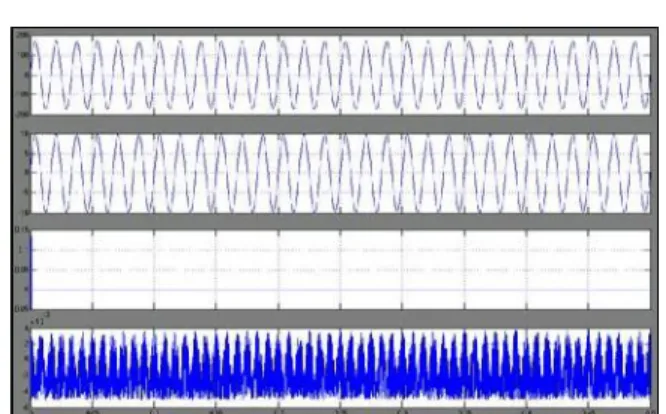
Fig. 16 shows the simulation results of the grounding voltage and the leakage current of the proposed transformerless grid-connected power converter. A capacitor and a resistor are connected in series and then connected between the ground and the solar cell array to simulate the parasitic effect of the solar cell array. As seen in Fig. 16(c), the negative terminal voltage of the solar cell array with reference to the ground is about 0 V and contains nearly no high frequency component.
Fig. 16. results of the grounding voltage and the leakage current of the proposed transformerless grid-connected power converter. (a) Utility voltage. (b) Output current of the dc–ac inverter. (c) Voltage
of the negative terminal of the solar cell array referred to the ground. (d) Leakage current.
The leakage current ig , passing through the simulated capacitor and resistor, is shown in Fig. 16(d). It is smaller than 10 mA. Because of the small ripple for the negative terminal voltage of the proposed transformerless grid-connected power converter, the leakage current complies with the requirement stated in the VDE 0126-1-1 standard [25]. This effectively demonstrates that the proposed transformerless grid-connected power converter can not only solve the problem of TCO corrosion but also the problem of leakage current.
VIII. CONCLUSION
IX. REFERENCES
[1] T. Suntio, J. Leppaaho, J. Huusari, and L.
Nousiainen, “Issues on solargenerator interfacing
with current-fed MPP- tracking converters,” IEEE
Trans. Power Electron., vol. 25, no. 9, pp. 2409–
2419, Sep. 2010.
[2] S. L. Brunton, C.W. Rowley, S. R. Kulkarni, and
C. Clarkson, “Maximum power point tracking for
photovoltaic optimization using ripple-based extremum seeking control,” IEEE Trans. Power
Electron., vol. 25, no. 10, pp. 2531–
2540, Oct. 2010.
[3] L. Maharjan, S. Inoue, H. Akagi, and J. Asakura,
“State- of-charge (SOC)- balancing control of a battery energy storage system based on a cascade
PWM converter,” IEEE Trans. Power Electron., vol. 24, no. 6, pp. 1628–1636, Jun.
2009.
[4] J. M. A. Myrzik and M. Calais, “String and
module integrated inverters for single-phase grid connected photovoltaic systems—a review,” in Proc.
IEEE Bologna Power Tech Conf., Jun. 23–26, 2003, vol. 2, pp. 1–8.
[5] J. Leppaaho and T. Suntio, “Dynamic
characteristics of current-fed superbuck converter,”
IEEE Trans. Power Electron., vol. 26, no. 1, pp. 200–
209, Jan. 2011.
[6] A. Koran, K. Sano, R. Y. Kim, and J. S. Lai,
“Design of a photovoltaic simulator with a novel reference signal generator and two-stage LC output
filter,” IEEE Trans. Power Electron., vol. 25, no. 5,
pp. 1331–1338, May 2010.
[7] U. Boeke and H. van der Broeck, “Transformer -less converter concept for a grid-connection of
thin-film photovoltaic modules,” in Proc. IEEE Ind.Appl. Soc. Annu. Meet., Oct. 5–9, 2008, pp. 1–8.
[8] Y. Sozer and D. A. Torrey, “Modeling and
control of utility interactive inverters,” IEEE Trans.
Power Electron., vol. 24, no. 11, pp. 2475–2483, Nov. 2009.
[9] Z. Liang, R. Guo, J. Li, and A. Q. Huang, “A
high-efficiency PV module integrated DC/DC converter for PV energy harvest in FREEDM
systems,”IEEE Trans. Power Electron., vol. 26, no. 3, pp. 897–909, Mar. 2011.
[10] A. Chen, W. Wang, C. Du, and C. Zhang,
“Single-phase hybrid clamped three-level inverter
based photovoltaic generation system,” in Proc. IEEE
Int. Symp. Power Electron. Distrib. Generation Syst., Jun. 16–18, 2010, pp. 635–638.
GOUTHAMI DIXITH A currently pursuing her M.Tech in Electrical Power Systems in Balaji institute of Technology and Sciences, Warangal, Telangana, India affiliated to JNTU University, Hyderabad. She has done her B.Tech degree from Balaji institute of Technology and Sciences, affiliated to JNT University, Hyderabad, Telangana, India and her fields of interest include Renewable Energy Sources, Power Systems and Neural Netorks.