Photovoltaic System with Step Up Converter
1Bhushan S. Chaudhari,2M. Mujtahid Ansari,3Nilesh S. Mahajan
1. Research Scholar,Electrical Engineering Dept, SSBT‘s COET, Jalgaon (MS),India. 2. Assistant Professor, Electrical Engineering Dept, SSBT‘s COET, Jalgaon (MS), India. 3. Assistant Professor, Electrical Engineering Dept, SSBT‘s COET, Jalgaon (MS), India.
[email protected] , 2. [email protected], 3. [email protected]
Abstract- A novel step up converter which is proposed
for a front end photovoltaic power system. Through a voltage multiplier module in which an asymmetrical interleaved step up converter usually high step up gain without which act as a function at an extreme duty ratio. The voltage multiplier module which is create of a conventional boost converter and coupled inductors. An extra conventional boost converter is combine into the first phase to achieve a considerably higher voltage conversion ratio. The two phase configuration not only decreases the current stress through each power switch but also force to do some thing the input current ripple, in which decreases the conduction losses of MOSFETs. The proposed step up converter functions as an active clamp circuit which moderate large voltage spikes across the power switches. So, the low-voltage rated MOSFETs which can be adopted for reduces of conduction losses and also cost. Efficiency improves because the energy which is stored in leakage inductances is energized to the output terminal. Finally, the prototype circuit which with a 40V input voltage, 380V output is operated to verify its performance. The highest efficiency of the step up converter is 96.8%.
Keywords: Step up converter, photovoltaic system,
voltage multiplier module, MPPT model, PWM converter.
I. INTRODUCTION
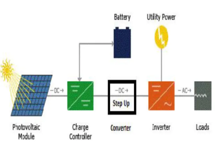
Fig. 1 Typical photovoltaic system
A photovoltaic system also known as solar PV power system or simply PV system which is a power system designed to supply usable solar power by means of photovoltaics. PV system consists of an arrangement of several components which are as including solar panels to absorb and convert sunlight into electricity and a solar inverter to change the electric current from DC to AC, as well as having mounting cabling and other electrical accessories to set up a working system. But the output voltage of PV system is very low so to get large output a step up converter are using here to boost the output voltage with voltage multiplier [1] [2]. The typical PV system is shown in above figure. It use a solar tracking system to improve the system's overall performance and also include an integrated battery solution. A solar array which is only encompasses the ensemble of solar panels and the visible part of the PV system also does not include all the other hardware, often summarized as balance of system PV systems convert light directly into electricity and which should not be confused with other technologies such as concentrated solar power or solar thermal or used for heating and cooling [6].
II. PROPOSED TOPOLOGY
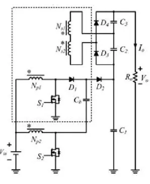
Fig. 2 Step up converter
The proposed high step-up converter with voltage multiplier module is shown in Figure. A conventional boost converter and two coupled inductors are located in the voltage multiplier module, which is stacked on a boost converter to form an asymmetrical interleaved structure. Primary windings of the coupled inductors with Np turns are employed to decrease input current ripple, and secondary windings of the coupled inductors with Ns turns are connected in series to extend voltage gain. The turns ratios of the coupled inductors are the same.
The Figure number 2 shows the circuit configuration of the proposed an asymmetrical interleaved converter with voltage multiplier cell. The voltage multiplier module of the proposed converter is composed of coupled inductor, the conventional boost converter and a voltage-lift capacitor. This capacitor offers an extra voltage conversion ratio. The leakage energy of the coupled inductor is recycled to the output capacitors the turns ratio of coupled inductors can be designed to enlarge voltage gain. The number of multiplier can be adjusted to get a desired duty ratio; a higher boost rate is easily obtained from the voltage multiplier. The coupling coefficient of the coupled inductor is denoted [5].
III. OPERATING PRINCIPLE
The switching period can be subdivided in to six modes of operation. The modes 1-3 are same as modes 4-6. So the first three modes are explained here. To make the circuit operation simpler, some assumptions are made the transformer leakage inductances are negligible The magnetizing inductances Lm1 and Lm2 are identical. The
phase shift between two switches are 1800The proposed converter operates in continuous conduction mode.
Fig.3 Operating modes of converter
A. Mode I
At t=t0 , the power switches S1 and S2 are both turned ON. All of the diodes are reversed-biased. Magnetizing inductors Lm1 and Lm2 as well as leakage inductors Lk1 and Lk2 are linearly charged by the input voltage source
Vin .
B. Mode II
At t=t1 , the power switch S2 is switched OFF, thereby turning ON diodes D2 and D4 . The energy that magnetizing inductor Lm2 has stored is transferred to the secondary side charging the output filter capacitor C3 . The input voltage source, magnetizing inductor Lm2 , leakage inductor Lk2 , and voltage-lift capacitor Cb release energy to the output filter capacitor C1 via diode
D2 , thereby extending the voltage on C1 .
C. Mode III
At t=t2 , diode D2 automatically switches OFF because the total energy of leakage inductor Lk2 has been completely released to the output filter capacitor C1. Magnetizing inductorLm2 transfers energy to the secondary side charging the output filter capacitor C3 via diode D4 until t3 .
At t=t3, the power switch S2 is turned ON and all the diodes are turned OFF. Now all the diodes are reversed-biased and the Magnetizing inductors Lm1 and Lm2 as well as leakage inductors Lk1 and Lk2 are linearly charged by the input voltage source Vin.
E. Mode V
At t=t4, the power switch S1 is turned OFF, therefore diodes D1 and D3 are turned ON. Now the energy stored in the magnetizing inductor Lm1 is transferred to the secondary side and it charges the output filter capacitor
C2. The input voltage source and the energy stored in the
magnetizing inductor Lm1 is completely released to the voltage-lift capacitor Cb through the diode D1, which supplies extra energy to Cb.
F. Mode VI
At t=t5, the diode D1 is automatically turns OFF because the entire energy stored in the leakage inductor Lk1 is totally released to voltage-lift capacitor Cb. Now the magnetizing inductor Lm1 transfers energy to the secondary side and it charges the output filter capacitor
C2 through the diode D3 until t0.
Fig..4 Steady waveforms of the proposed converter at CCM.
Above figure 4 shows the steady waveforms for step up converter at its different operating modes which is at continuous conduction mode.
V. DESIGN AND EXPERIMENTAL RESULTS
Fig. 5 Matlab simulation model for step up converter
COMPONENTS SYMBOLS PARAMETERS
Magnetizing Inductances
Lm1, Lm2 133 uH
Leakage Inductances
Lk1, Lk2 1.6 H
Turns Ratio N(Ns/Np) 1
Power Switches S1, S2 IRFP4227
Diodes D1, D2, D3, D4 FCF06A-40
Capacitors Cb, C1, C2, C3 220 uF
Table 1 Parameters and symbols
are given. Its simulation waveform are given in following figure
Fig. 6 Voltage and current waveforms for Vgs1, Vgs2, ILK1, ILK2
Figure 6 illustrates the measured waveforms of voltages at switch S1 ( Vgs1) and switch S2 (Vgs2) and current at Leakage inductances Lk1 and Lk2.
Fig. 7 Voltage and current waveforms for Vgs1, Vgs2, Id1, Id2
Figure 7 shows the waveforms for voltages at switch S1 ( Vgs1) and switch S2 (Vgs2) and current at diodes D1 & D2.
Fig. 9 Voltage and current waveforms for Vgs1, Vgs2, Id3, Id4
Figure 9 depicts the voltage and current waveforms at the Swith S1 , S2 and Current at diodes D3 and diode D4.
Fig. 10 Results for current waveforms for Iin, Ilk
Fig. 11 Results for output voltages Vcb, Vc1, Vc2, Vc3
Figure shows the waveforms for output voltages at four capacitors Cb, C1, C2 and C3.by addition of these output voltages we get the output voltage of step up converter.
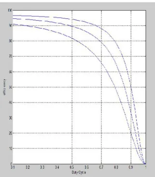
Fig. 12 Efficiency versus duty cycle.
Figure 12 plots the waveform for efficiency versus duty cycle of the proposed converter which shows the maximum efficiency is 96 %.
The output voltage of step up converter is the sum of all the voltages across the capacitors which is shown in
figure number 18. So the output voltage is 380V. The figure shows the efficiency of proposed step up converter.
VI. CONCLUSION
This paper has presented the topological principles steady state analysis and experimental results for a proposed step up converter. The proposed step up converter has been successfully implemented in an efficiently high step up conversion The experimental results which indicate that leakage energy is recycled through capacitor Cb to the output terminal. The voltage stresses over the power switches are restricted and are much lower than the output voltage (380 V). These switches, conducted to low voltage rated and low on-state resistance MOSFET, can be selected. Furthermore, the full-load efficiency is 96.8% at Thus, the proposed converter is suitable for PV systems or other renewable energy applications that need high step up high-power energy conversion. The simulation results by using MATLAB Simulink proved the validity of the theoretical analysis and the feasibility of the proposed step up converter.
REFERENCES
[1] Kuo-Ching Tseng, Chi-Chih Huang, and Wei-Tuan Shih “A High Step-Up Converter With Voltage Multiplier Module For a Photovoltaic Power System” IEEE Transactions On Power Electronics, Vol. 28. No. 6, June 2013. 3047.
[2] Bhushan S. Chaudhari, M.M. Ansari, N.S. Mahajan, “A Review Of Step Up Converter With Voltage Multiplier For Photovoltaic Power System” , International Journal of Innovative Research in Advanced Engineering (IJIRAE), Issue 11, Volume 2 (November 2015), ISSN: 2349-2163.
[3] Yen-Mo Chen, Alex Q. Huang, Xunwei Yu, “A High Step-Up Three-Port DC–DC Converter for Stand-Alone PV/Battery Power Systems”, IEEE Transactions On Power Electronics, Vol. 28, No. 11, 0885-8993, November 2013.
[4] Vincent W. Ng, Seth R. Sanders, “A High-Efficiency Wide-Input-Voltage Range Switched Capacitor Point-of-Load DC–DC Converter”, IEEE Transactions On Power Electronics, Vol. 28, No. 9, 0885-8993, September 2013.
[5] Chung-Chuan Hou, , Chih-Chung Shih, Po-Tai Cheng, Ahmet M. Hava, “Common-Mode Voltage Reduction Pulsewidth Modulation Techniques for Three-Phase Grid-Connected Converters”, IEEE Transactions On Power Electronics, Vol. 28, No. 4, 0885-8993, April 2013.
[7] Shih-Jen Cheng, Yu-Kang Lo, Huang-Jen Chiu, Shu-Wei Kuo, “High-Efficiency Digital-Controlled Interleaved Power Converter for High-Power PEM Fuel-Cell Applications”, IEEE Transactions On Industrial Electronics, Vol. 60, No. 2, 0278-0046, February 2013.
[8] Rong-Jong Wai, Kun-Huai Jheng, “High-Efficiency Single-Input Multiple-Output DC–DC Converter”, IEEE Transactions On Power Electronics, Vol. 28, No. 2, 0885-8993, February 2013.
[9] Fellipe S. Garcia, Jose Antenor Pomilio, Giorgio Spiazzi, “Modeling and Control Design of the Interleaved Double Dual Boost Converter”, IEEE Transactions On Industrial Electronics, Vol. 60, No. 8, 0278-0046, August 2013.
[10] Hongrae Kim, Babak Parkhideh, Tim D. Bongers, Heng Gao, “Reconfigurable Solar Converter: A Single-Stage Power Conversion PV-Battery System”, IEEE Transactions On Power Electronics, Vol. 28, No. 8, 0885-8993, August 2013.
[11] Jia-Min Shen, Hurng-Liahng Jou, Jinn-Chang Wu,
“Novel Transformerless Grid-Connected Power Converter With Negative Grounding for Photovoltaic Generation System”, IEEE Transactions On Power Electronics, Vol. 27, No. 4, 0885-8993, April 2012. [12] Wuhua Li, Jianguo Xiao, Yi Zhao, Xiangning He,
“PWM Plus Phase Angle Shift (PPAS) Control Scheme for Combined Multiport DC/DC Converters”, IEEE Transactions On Power Electronics, Vol. 27, No. 3, 0885-8993, March 2012. [13] J.S.Anu Rahavi, T.Kanagapriya, Dr.R.Seyezhai,
“Design and Analysis of Interleaved Boost Converter for Renewable Energy Source”, International Conference on Computing, Electronics and Electrical Technologies, IEEE, 978-1-4673-0210-4112, 2012 . [14] Juan Manuel Carrasco, Leopoldo Garcia Franquelo,
Jan T. Bialasiewicz, Eduardo Galván, Ramón C. Portillo Guisado, , Ma. Ángeles Martín Prats, José Ignacio León, and Narciso Moreno-Alfonso, “Power -Electronic Systems for the Grid Integration of Renewable Energy Sources: A Survey”, IEEE Transactions On Industrial Electronics, Vol. 53, No. 4, 0278-0046, August 2006.
[15] Y. Xiong, X. Cheng, Z. J. Shen, C. Mi, H. Wu, and V. Garg, “A Prognostic and Warning System for Power Electronic Modules in Electric, Hybrid, and Fuel Cell Vehicles”, IEEE Transactions, 1 -4244-0365-0/06, 2006.
BIOGRAPHIES
Mr. Bhushan S. Chaudhari received
the B.E. Electrical from Government College of Engineering, Jalgaon, in 2013, and pursing M.E. from S.S.B.T.’s College Of Engineering and Technology, Jalgaon. He has published one paper in international journal.
M. Mujtahid Ansari received his B.E.(
Electrical Engg) and M.E.(Electrical Power System) from the S.G.B.University, Amravati, India in year 1996 and 2009 respectively . He is member of IE, ISTE and IACSIT. He has joined SSBT’s College of Engineering and Technology, Jalgaon in the year 2000 where he is working as Assistant Professor in Electrical Engineering Department. He has published six papers in international journal and one text book. He was chairman Board of studies in Electrical Engineering and Instrumentation Engineering under the faculty of Engineering and Technology, North Maharashtra University, Jalgaon (MS) India.
Nilesh S. Mahajan had completed his M.