Digital Technical Journal
Digital Equipment Corporation
Cover Design
.S)'stems based un Digital's aduanced CMUS technology are featured in Ibis issue. Tbe graphic on our COI'er includes the lattice structure of the silicon nystal. a basic element of this tecbnology. The expansion of the image expresses the pe1j'ormance growth and the system e.Yiensibility of the new CVAX-based systenH.
The COI'er was designed by Barbara Grzeslo and]acquie Hockaday 1�[ the Graphic Design Department.
Managing Editor Richard W Beane Editor
jane C. Blake Production Staff
Produnion Editor-Helen L. Paucrson Designer- Charlo!!<: Bell
Typographers-Jonathan !\·f. Uohy Margart:t Burdine lllustrawr- Dt:borah Keeley Advisory Board
Samuel H. Fuller, Chairman
Robert M. Glorioso John W McCredie
Mahendra R. Patel F. Grant Saviers William D. Strecker Victor A. Vyssotsky
The Digital Tecbnical jnumal is published by Digital Equipmt:nt Corporation. 77 Reed Road. Hudson. Massachuscus 01749.
Changes of address should be sent to Digital Equipment Corporation. aut:ntion: List Maintenance.
I 0 Forbes Road. Northboro. MA 0 15j2. Please includt: the address label with changes marked.
Comments on the content of any paper are wclcomt:d. Write to the editor at Mail Stop 1-lLOl-.�/Kil at the published-by address. Comments can also be sent on the ENET to RDV�'X::OIAKE or on the ARPANET to BLA.K.E'X,RDVAX. DEC�)l)ECWRL.
Copyright © 1988 Digital Equipment Corporation. Copying without fee is permiued providt:d that such
copies are made for use in t:duc:uional institmions by faculty members and arc not distributed for commercial advamage. Abstracting with credit of Digital Equipment Corporation's authorship is pcrmiued. Requests for other copies for a fee may be made 10 Digital Press of Digital Equipmem Corporation. All rights reserved. The information in this journal is subject to change without notice and should not be construed as a com miunem by Digital Equipment Corporation. Digital Equipment Corporation assumt:s no responsibility for any errors that may appear in this document. lSSN 0898-90 1 X
Documentation Number EY-67•i2E-DI'
The following are trademarks of Digital Equipment Corporation: ALL-IN- I. DEQNA. HSC70. J-1 l. MicroVAX, MicroVAX 11, MicroVAX .�000. N•'-'11. NOTES. Q-bus, Q22-bus, RA81. RA82, RD54. RQDX3. RX50. TK50. UITRIX-.�2. VAX. VAX-11/780. VAX-11/782. VAX 6200. VAX 6210, V�'( 6220. V�'( 62.10. VAX 6240. VAX 8200, V�'( 8300. VAX 8650. VAX flf!OO. VAX HH40. VAXlll, VAXELN. V�'( MACRO, V�X SI'M. VAX/VMS. VMS.
Compu-Sharc is a trademark of Compu-Shart:. Inc. GDS 11 is a trademark of Calma Corporation. SPICE is a trademark of the University of California at lkrkdey
8 Foreword
Robert M . Supn i k
1 0 An Overview of the VAX 6200 Family of Systems Brian R. All ison
CV AX-based Systems
19 The Architectural Definition Process of the VAX 6200 Family Brian R. Al l ison
28 Interfacing a VAX Microprocessor to a High-speed Multiprocessing Bus Richard B . GiUett, Jr.
4 7 The Role of Computer-aided Engineering in the Design of the VAX 6200 System
Jean H. Basma j i , G lenn P. Garvey, Masood Heydari , and Arthur L. Singer
57 VMS Symmetric Multiprocessing Rodney N . Gamache a nd Kathleen D . Morse
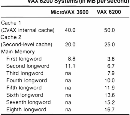
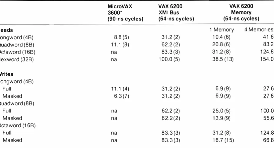
64 Performance Evaluation of the VAX 6200 Systems B hagyam Moses a nd Karen T. DeGregory
79 Overview of the MicroVAX 3500/3600 Processor Module
Gary P Lidi ngton
87 Design of the MicroVAX 3500/3600 Second-level Cache
Charles]. DeVane
95 The CVAX 78034 Chip, a 32-bit Second-generation VA X Microprocessor Thomas F. Fox , Pau l E . Gronowski , Ani! K. Jai n , Burton M . Leary, a nd
Daniel G . M i ner
1 09 Development of the CVAX Floating Point Chip
Edward J . McLe l la n , G i l bert M . Wolrich, and Robert AJ Yod lowski
121 The System Support Chip, a Multifunction Chip for CVAX Systems Jeff Winston
129 Development of the CVAX Q22-bus Interface Chip
Barry A. Maskas
Editor�s Introduction
Jane C. Blake Editor
The second issue of the Digital Technical journal (March I 986) fearured papers on the then recently announced MicroVAX II system, a system based on a single-chip VA.'{ implementation. In this seventh issue, we present papers on the sec ond generation of that chip set, CVA.'\, the two new systems that take advantage of its increased performance capabilities, and a new version of the VAXfVMS operating system for symmetric multiprocessing.
The new mid-range system based on the CVAX chip set is the VAX 6200 family of compUlers, which utilizes a multiprocessing architecture. The first of rwo papers by Brian Allison is an overview of this highly configurable, expandable system. Brian's second paper offers insights into the architectural definition process for the 6200. One of the major decisions made by the 6200 engineers was to design a new interconnect to support the multiprocessor system. Rick Gillett presents an informative discussion of the com plexities involved in interfacing a microprocessor ro a high-speed, multiprocessing bus.
To ensure the availabiliry of first-pass func tional parts, a design verification team of engi neers worked in parallel with the 6200 module designers. Jean Basmaji, Glenn Garvey, Masood Heydari, and Art Singer discuss the computer aided engineering and verification principles the team instituted for the project.
Rod Gamache and Kathy Morse then describe the major features of symmetric multiprocessing in the VAXjVMS operating system. Of particular interest is their description of a new synchroniza tion method implemented in VAXjVMS version 5.0.
2
In the last paper related ro the VAX 6200 system, Bhttgyam Moses and Karen DeGregory describe the development of workloads to measure VAX 6240 performance. As part of their discussion, they include performance measurements and analysis. The second new system based on the CVAX chip set is the low-end MicroVAX -�500/3600 system, which offers three times the performance of irs predecessor, the MicroVAX II. In his over view of the major sections of the processor mod ule, Gary Lidington relates how schedule and performance requirements influenced product design decisions.
Charles DeVane then describes the MicroVAX
.3500/3600 system's rwo-level cache architecture, with emphasis on the design of the second-level cache. He also presents some cache performance rest results.
The high performance of both the VAX 6200 family and the MicroVAX 3500/3600 system is attributable in great measure tO the CMOS VAX family of chips on which these systems are based. Our five final papers address the design and development of this chip set. Frank Fox, Paul Gronowski, Ani! Jain, Mike Leary, and Dan Miner begin the discussion with an explanation of how designers achieved the performance goals for the single-chip VAX CPU by reducing ticks per instruction and machine cycle time.
A companion ro the CVAX CPU, the floating point processor chip offers floating point perfor mance equal ro that of the microprocessor for integer operations. The approach taken tO attain this goal and a description of the chip are pre sented by Ed McLellan, Gil Wolrich, and Bob Yodlowski.
Jeff Winston then discusses the development of the system support chip, which provides a com mon core of peripheral system functions.
Next, Barry Maskas relates the design effortS of three groups, one in Japan and two in the U.S., that resulted in a single-chip interface between the CVAX microprocessor and the Q22-bus l/0 subsystem.
Brian R. Allison Brian AJlison, a consultant engineer for mid-range VAX systems, was the system architect responsible for the coordination of the VAX 6200 system definition and design. Prior tO this work, he served as system architect for a project that yielded several products. including DEBNA, DEBNK, and the KA800. As a member of the VAX-11 /750 design team, he wrote various portions of the microcode for that product. Brian holds a BS.E.E. and a B.S.C.S. from Worcester Polytechnic Institute ( 1977).
jean H. Basmaji jean Basmaji is the technical director of computer-aided engineering and design-verification testing for the VAX 6200 project. A soft ware consultant engineer, he has also been involved with CAE/DVT planning and scheduling, and has served as CAE/DVT project leader for the VAX 6200 CPU module. jean joined Digital after receiving his B.S.E.E. from Lowell Technological Institute in 1977.
Karen T. DeGregory A senior software engineer in the Systems Perfor mance Analysis Group, Karen DeGregory is project leader of systems perfor mance measurement for the VAX 8840 and VAX 6240 systems. In addition to planning and implementing the measurements, she helped develop appro priate workloads for these systems. Prior to this work, Karen was a senior
software specialist in the Software Services Backup Support Group. She received her B.S. ( 1980) with honors and distinction and her M.S. ( 1981) from Cornell University.
Biographies
4
Thomas F. Fox Fran k Fox . a principal engi neer in the Sem iconducror Engi· ncering Group , worknl on rhc im ple mentation of the CVAX 780:14 CPU c h i p . He is currently design i ng a high-performance m icroprocessor and cons u l ting with the Advanced Sem iconductOr Development Group on t he deve lopment of a su bmicron CMOS process . Frank was educated i n I re land and rece ived a B . E . degree from University College Cork ( 1974) and a P h . D . degree from Trinity Col lege Dublin (1978) . both i n electrical engi neering. He has publ ished papers on ultrasonic i nstru mentation and magnetic reso nant i magi ng (M RI) and has three patents pend i ng.
Rodney N . Gamache A consulting software engineer i n r he VAXjVMS Soft· ware Development Grou p, Rod Gamache has been with Digita l for 1 1 years. Shortly after receiving a B . S . i n mathemat ics and com puter science from the Univers i ty of New Ham pshire , he joined Digital ro work on the development of DECnet Phases III and IV for both RSX- 1 1 M and VMS. For the last two years . Rod has been project l eader for t he VMS symmetrical multiprocessing project and has filed two pate nrs on VMS SMP. Rod also serves as a consu l tant for the architectures of fu ture low-end VA.,'( processors.
Glenn P. Garvey G lenn Garvey is an e ng i neering supervisor presently leading a team in the verification of a new VAX processor. He was t he project leader for the system-level veri fication pe rformed on the VAX 6 2 00 system and has been involved in model i ng and verification since coming to Digital i n 1 98 2 . Glenn was a co-op student a t Digital i n I 9 8 0 and 1 98 1 . H e holds a B . S . E . E . from Rensselaer Polytechnic I nstitute.
Richard B. Gillett, Jr. Rick Gillett, a consu ltant engi neer, led the VAX 62 00 CPU module project. Prior ro his work on the 6 2 00, he served as one of the arc hitects of the X M I bus and was a member of t he VAXB I bus project ream . Relative ro his work on rhe VAX 6 2 00 design , he has recently filed 1 3 patent applications. Currently, he is system arc h i tect for a new VAX system . Rick joi ned D i g i tal after receiving a B.S. E . E . (su m ma cum laude) from rhe Universi ty of New Hampshire in 1 9 7 9 . He is a member of Tau Beta Pi and Phi Kappa Phi .
a .36-bit system and has been respons ible for functional rest partern genera tion for several products. Most recently, he was responsible for CAD/DVT on the VAX 6 2 00 project . Masood holds a B.S. and an M.S. in computer engineer i ng from Boston Universi ry ( 1 980) . He is a member of Tau Beta Pi .
Anil K. Jain Ani ! Jai n received an M . S . E . E . from the University of Cincin nati (1980) and a B . S . E . E . from Pu njab Engineeri ng Col lege ( 1978) . Upon joi n i ng Digita l in 1 980 , he worked on bipolar and CMOS- 1 technology while a member of the Device Mode l ing Grou p . A5 a senior engineer working on the CVAX project, Ani ! designed the bus i nterface unit for the CPU c h i p and has a patent pend i ng for the bus i nterface protocol . He is currently working as a project leader on the float i n g point chip project for vector appl ications .
Burton M. Leary M i ke Leary is a princi pal engi neer i n t he Semiconductor Engineering Group/Advanced Deve lopment Memory Grou p and is currently working on the design of advanced memory products . In previous work, he partici pated in the design of the floating point c h i ps for the MicroVAX and 82 00/8 3 0 0 systems and the design of a CMOS serial i n terface controller c h i p . M i ke joined Digital after receiving a B . S . E . E . from the Unive rsity of Mas sachusetts . He is a member of Tau Beta Phi .
Gary P. Lidington Cu rrently an engineeri ng manager i n the MicroVAX Engi neering Grou p , Gary Lidi ngron has served as a system engi neer for the MicroYAX 3 5 00/3600 system and as a maintainabi lity engineering project manager for the MicroVAX II and si ngle-board computers with Q-bus multi processi ng arch itectu res. Before com i ng to Digital i n 198 1 , Gary was a co-op student and rest engineer on the L200 project at Teradyne, l nc . He holds a B . S . E . E . (honors) from Tufts U n i versity and an M .S . i n com puter engineering from the U n i versity of Massachusetts .
Barry A. Maskas Barry Maskas , a consulting engineer with the Semicon ductor Engineering Group, is the project leader for t he development of a cus tom VLSI memory contro.ller. Prior to his current work , he was the U S. project leader and architect for the CVAX Q 2 2 -bus i nterface c h i p and co designer of the Micro VAX IICPU and me mory boards. Barry came to Digi ta l i n
Biographies
Edward J. Mclellan Fd McLellan is a principal engineer in the Semicon· ductor Engineering Group. He has worked on the design of several chips, including the .J-1 I and the CVAX tloating point accelerator chips. He holds one patent for previous work and has made application for two additional patents based on work done for the CVAX tloating point chip. Ed joined Digital in 1980 after receiving a B.S. in computer and systems engineering from Rensselaer Polytechnic Institute. Currently he is project leader for a tloating point chip for a new pro cessor.
Daniel G. Miner Dan Miner came to Digital after receiving a B.S. in com· purer engineering from Rensselaer Polytechnic Institute in 198'5 A software engineer in the Semiconductor Engineering Group. he wrote the debug and diagnostic tests for the CVAX CPU chip. Dan co-authored and presented a paper on the subject of resrahi I i ty strategy at the I 987 IEEE International Test Conference.
David K. Morgan Dave Morgan is the engineering manager of Advanced Peripheral Development in the Semiconductor Engineering Group For his work on several engineering projects. Dave has three patents pending. Before joining Digital in 197'5, he was a design engineer at the RCA Solid State Division and holds five parents for his work on integrated circuit designs. Dave receiwcl a B.S.E.E. ( 1969) from Western New England College, an M.S.E.E. ( 1972) from Rutgers University. and has pursued doctoral work in sol id·state physics.
Kathleen D. Morse A-; a consulting software engineer. Kathy Morse is working on advanced development for the VA.X.jVMS Development Group. She is one of the VMS SMP architects and consults on enhancements to vari· ous parts of the VMS executive. Earlier, she implemented the VMS support for the first MicroVA.t'{ systems, the first asymmetric multiprocessing VAX sys· rem. and the i'v1A780 mulriporr memory. Kathy joined Digital in 1976 after receiving her B.S.CS degree from Worcester Polytechnic Institute. where she also earned her M.S.CS. degree in 1985. Kathy is a member of IEEE, the Professional. Council, and ACM as well as Tau Beta Pi and Upsilon Phi Epsilon.
8600 project. Before joining Digital i n I 984 , Art was employed by I PL Sys tems as a design engi neer and manager of a m icrodiagnosric development grou p Whi le at I PL, he received a parent for the des ign of an i nstruct ion u n i t . Hc is a mem ber of Tau Bcra Pi and Eta Kappa Nu .
Jeff Winston A mcmhcr of the Sem iconductor Engineeri ng Group , Jeff Winston designed thc microsequencer for the VAX 8 2 0 0 CPU c h i p and led the design of two generations of the M icro VAX System Support C h i p . He has also contributed to the development of many CAD tools used in c h i p design . Before joining D igital in 1980 . Jeff rcceived his B . S . ( 1 97 9 ) and M . S . ( 1 980) i n E l ectrica l Engi neeri ng from Corne l l University. He is current ly leading thc dcve l opment of the X M I i nt erface chip set for a new m i d-range VAX CPU.
Gilbert M. Wolrich A consu l t i ng engineer in t he Semiconductor Engineer i ng Group/Architectu rally Focused Logic, G i l participated in the )- 1 1 con trol c h i p design and was project leader for the CVAX CFPA and the J- 1 I FPA
c h i p projects. He holds a parent for an ALU with Carry Length Detection used on the J-11 FPA. G i l received a B . S . E . E from Rensse laer Polytechnic I nstitute i n 1 9 71 and an M . S . E . E . from Northeastern Un iversity i n 1 97 7 .
Robert AJ Yodlowski I3ob Yod lowski. a pri ncipal engi neer. is the chip i m p l ementation project l eader and l<:ad circu i t designer for the CVAX floating point acce lerator. For his work on this project , Bob has three patents pending. He was also sen ior circuit designer on the J- 1 1 float i ng poi n t c h i p project. Re lative t o this project work. he i s a co-i nventor ancl patent holder for AUJ with Carry Length Detection ( 1 987 ) . Before joining Digi ta l in l 9 7 7 , Bob was a sen ior member of t h e technical staff at LFE Corporation i n Wa ltham , MA. H e received a I3 . S . i n engineering physics from Corne l l Un iver sity ( I 9 6 8 ) and an M .S . E. E. from Syracuse Un iversity (I 970 ) .
Foreword
Robert M. Supnik Corporate Consultant,
VLSI Technology, and Group Manager,
Semiconductor Engineering Microprocessor Development
In May 1985, Digital i ntroduced the MicroVAX II computer system . Based on the M icro VAX proces sor chip set, the M icroVAX II system offered unsurpassed price , performance. and re l iabi lity characteristics . In the three years si nce then, Digital has sold more tha n 1 00 , 0 00 systems based on the M icroVAX chip set. There are more M icroVAX -based systems in the field than a l l other types of VAX systems combined.
ln the same three years, t he practice of com puter engineering has advanced considerabl y . Faster processors, bigger memories, qu ieter pack ages , and more complex software have appeared in a steady stream . For Digital to remain com pe titive, we wou ld need, over t i me, a second gener ation of VLSI-based VAX c h i ps and systems . The chips and systems that constitute the second VLSI-based generation are described in this issue of the D igita l Technical]ou rnal .
The p lanning for the second generation began in 1983. That year, the LSI Group (now Sem icon ductOr Operations) formu lated a mu ltiyear pro gram for the deve l opment of both semiconductOr process technology and lead i ng-edge chip prod ucts . The key characteristics of this p rocess; product plan were
• CMOS (complementary metal -oxide-sem icon ductOr) p rocess technology (Previous Digita l c h i ps were based on NMOS technol ogy . )
8
• Multiple process generations rel ated by opt i
c a l sca l i ng
• VAX microprocessors as the leadi n g edge chip
deve lopment projects
• Performance i mprovements targeted for greater
than 50 percen t per year
This program not only provided the LSI Group with an overa l l structure for its process and c h i p development projects ; i t also provided Digital's system groups with a stable, long-term bas is for planning system products.
The program was a lso a significant leap of fai t h . When it was formu lated, there was no M icroVAX busi ness . The MicroVAX II system was two years away from s h ipment. Almost a l l design resources in the LSI Group and i n t he low end sys tem groups were busy with the MicroVAX chip set and its related systems. Major development projects in technology, chip design, systems design , and manufacturing were req u i red to bring the program vision to fru i t ion.
Work began with development of the u nder lying semiconductOr technology. Start i ng in
1983, a ream from Semiconductor Manufactur i ng's Advanced Semiconductor Development (ASD ) defined, simu lated, and rested CMOS-I , D i gital's first CMOS process. When first defined, CMOS-I 's key features - N - wel l base on a p-rype epitaxial layer. rwo levels of metal interconnect , 2 . 0 micron feature size, di rect scalabi lity to 1 . 5 micron feature sizes - were controvers i a l within a n i ndustry that was stil l debating N MOS versus CMOS . Over ri me, t hese choices have been vindicated , and CMOS-I has p roven ro be a main stream , robust, h ighly manufacturable process .
second-generation c h i p set (called CVAX) in mid-1984. The overarc hing goal was simple: three ti mes the performance of the MicroVAX chip set i n less than t hree years - a compound performance growth rate of more t han 50 per cent per year The central processor design starred from the MicroVA..'<: base but drew upon ideas from other VAX implementations, notab ly the 8700. The tloari ng poi n t u n i t design focused on m i n i mal execu tion flows for the most common instructions. Both chips rransirioned to i mple men tation in 1985 .
The origi nal concept for the CVAX chip set had been to bui ld chip- for-chip analogues of MicroVAX - a central processor and a floating point u n i t . However , as the flex i b i l i ty of the new CMOS process, and the effic iency of the CAD tools, were appreciated by designers , the chip set concept expanded beyond the central processor ro i nclude key peri pherals. The i mplementation of t hese peripheral functions i n VLSI chips made systems faster. more re l i ab le, and less expensive. In add i t ion . it allowed peripheral functions to be standard ized across multiple system i mplementa tions and add it ional fu nctions tO be added in modu lar fas hion . The Sem iconductor Engineer ing peripherals group (now Advanced Deve lop ment) speci fied and i m p lemented a memory con trol ler, a memory driver, a console i nterface, and a Q-bus interface.
Mter the MicroVAX I I system shipped i n May 1985. the Low-end Systems Group and the Mid range Systems Group became active l y involved in the specification of the CVAX c h i ps and in the defi n i tion of new systems u t i l i z i ng the chip set . I n the l ow end , the 3 5 00/3600 systems were defined as evol utionary extensions of the MicroVAX I I . Nonethe less, the performance targcts for the new chips posed knotty design problems for a system fami ly bounded by both cost and packagi n g considerations.
In the mid - range, the system designers wished to exploit the CVAX chip set's combination of high performance and low cost by constructing
and new system packagi ng ro su pport the con cep t . However, a genera l-purpose multiprocessor system was feasible only i f the VMS operating sys tem cou ld rake advan tage of the incrementa I power offered by addi t ional processors. This req u irecl a major restructuring of VMS tO su pport symmetric (al l processors equal ) mul ti proces s i ng. Thus, the defin i t ion and i mplementation of the mid-range 6 2 00 system fam i ly and of VMS symmetric mu lti processi ng su pport had to be close ly li n ked .
As the engineeri ng development projects pro gressed . manufacturing became heavily involved in p lann i ng and executing the transi tion from design to volu me product. LSI Manufacturing i n Hudson , Massachusetts, i ntroduced CMOS-I i nto mu ltiple fabrication units in order to produce prototypes qu ickly and ro ramp up to high vol ume production. System manufactur i ng groups in Westfield (Massachusetts) . AJbuq uerque (New Mexico). Puerto Rico, a net other sires worked close ly with rhe system designers to i ntroduce rhe new manufactur i n g processes requi red for system production .
The resu lts of these development programs is a family of VAX sysrems with exemplary price . per formance. and rel iab i l i ty characteristics. More over, the programs leave as residuals a set of VlSI com ponents from which other products can be bui l t , and base technology from which further advances i n chip and sysrem design wi ll evolve . The i n i tial program vision has been fu lfi ll ed, even exceeded . Many people, i n reams and indi vidually. worked together ro bri ng this abou t . The excel lence of the results refl ects. i n fu l l measun:. the exce llence of the work that t hey have done .
Brian R. Allison
I
An Overview of the
VAX 6200 Family of Systems
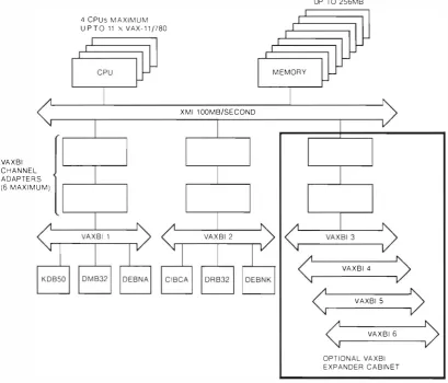
Digital's VAX 6200 series is a high-performance, expandable family of computer systems that combines low-cost microprocessors with high performance memory and I/0 subsystems. Based on the CMOS VAX chip set, the VAX 6200 CPU module performs at 2.8 times the VAX-11j780 system; utilizing a multiprocessing architecture, system speeds are available up to 11 times the VAX-11/780 system. The memory subsystem utilizes a multi controller architecture for up to 256MB of total system memory. The XMI bus, the electrical interconnect for the system, supports the multiple pro cessors, memory subsystems, and VAXBI channel adapters. The VAXBI is used for all IjO devices.
The VAX 6200 fami ly of computer systems is thc most reccn r audi tion to Digital's !inc of VA..'< com purer systems The VA,'( 6 200 systems. primari ly based on CMOS technol ogy, are mid-range sys tems which expl o i t mu l t iprocess i ng tech n i ques. The VA,'( 6200 fam i ly current ly comprises four systems, all bui l t from common subassembl ies. Any VAX 6200 system may be upgraded to any other VAX (1 200 system simpl y by adding CPU
and me mory modu l es to rhe existing cabi net. This paper provides an overview of the system and therefore a conrexr for the five papers that fol l ow i n this issue. These papers descri be sev eral of the components in detai l . the engi neering design cfforr, rhe performance eval uation pro cess, and some of the mult iprocess i ng aspects of the operating system .
In the pasr. CMOS- based m icroprocessor tech nology has been used pri mari ly ro b u i l d low-cost systems. Today , by using m u l ti p l es of these l ow cost m icroprocessors . we are presented a u nique opportu ni ty ro produce a high - performance com purer system when the microprocessors are cou pl ed with high-performance memory and 1/0 subsystems. Al t hough this type of system archi tect ure wi l l nor d i rectl y resu l t i n faster execut ion of a si ngle task, it docs result in greater system throughput i n app l ications t hat have several simu l taneously computabl e tasks. The architec ture cou p l es the effectiveness of the VMS operat i n g system in mu l t i program med environ ment s
1 0
with hardware opti m ized for effic ient m u l t i pro cessor operation . The result is a syste m that offers simi l ar performance for a large class of app l i ca tions at a better price-performance rat io than that offered by t radi t ional single-processor. h igh-per formance computer systems.
A pri mary objective of the VAX 62 00 system design is tO provide a h i g h l y configurable and expandab le computing environ men t . To ac hieve this objective . designers chose a modu lar sub asse mbly design for the totaJ syste m . This mod u lar design provides for cost-effect i ve bas ic sys tems and also al lows for system expansion to achieve higher performance. Al l mem bers of t he VAX (>2 0 0 fami ly arc housed in the same cabi net and usc the same basic su basse mbl ies. The on ly d i fference is t he nu mber of p rocessors, amount of memory . and num ber of 1/0 devices. Tab le I clerai Is the configurations of the VAX 6210 , VAX (1 2 2 0 , VAX 6 2:)0, and VAX 6 2 4 0 systems.
System A rchitecture
Al l VAX 6 2 0 0 systems cons ist of CPU (s ) , mem ory. and 1/0 channel adapters con nected to a common system i nterconnect known as the XMI . The VAXB I is used as the i nterconnect to a l l I/0 devices i n the system . 1 All memory and 1/0 devices are equal ly accessi b l.c by all CPUs in the syste m. Figure I shows a b l ock-level diagram of
the VA,'( 6 200 system.
Digital Technical jounwl
Ta ble 1 VAX 6200 Family System Configurations
Number of processors
M ain m emory VAXBI channels
CPU cycle time Cache size
(per CPU) Free XMI slots Performance (times one
VAX-1 1 /780 system) Maximum CPUs
Maximum memory Maximum VAXBI channels
VA X B I C HA N N E L ADAPTERS
(6 M AX I M U M)
VAX 6210 VAX 6220
1 2
3 2 M B 64 M B
2 2
80 ns 80 ns
1 KB 1 KB
256KB 256KB
1 0 8
2.8 5.5
4 4
256MB 256MB
6 6
4 CPUs M A XIM U M
U P T O 1 1 X VAX- 1 1 /780
X M I 1 00 M B/SECOND
VAX 6230 VAX 6240
3 4
64 M B 128MB
2 2
80 ns 80 ns
1 KB 1 KB
256KB 256KB
7 4
8.3 1 1 .0
4 4
256MB 256MB
6 6
UP TO 256MB
<
<
<
VA X B I 4
>
VAXBI 5
>
VA X B I 6
>
OPT I O N A L VA X B I EXPANDER C A B I N E T
Figure 1 VAX 6200 System Block Diagram
Digital Technical journal I I
[image:13.595.89.499.331.681.2]--- A n Overview of the VAX 6200 Family of Systems
The primary goa l of the VAX 6 2 0 0 system is to a l low higher l evels of system performance through multiprocessing. To s i m p l i fy software design and to be consistent with previous mul t i processor architecture , it was essentia l to pro vide a shared memory resource . All system mem ory is a global resource accessible through the same address space from each processor and from a l l ljO devices. A sophist icated mu l t i l evel cache contai ned l oca l ly i n each CPU m i n i m i zes mem ory accesses on the X M I . Cache coherency is maintained tota l ly by hardware .
Technology
The VA..'\ 6 2 00 systems are based on a nu mber of d ifferent CMOS technologies . The VAX CPU c h i p s e t and t h e system interconnect transceivers are i mplemented entirely in Digita l 's ful l custom CMOS process featuring a size of 1 . 5 m icrons 2
The i nterface between each mod u l e and the system i nterconnect is impl e mented in channel l ess 1 . 5 - micron CMOS gate arrays . The nu mber of gates used i n these arrays varies from 1 8K to 5 0 K gates . The i nterface t O the VAXBI and the X M I arbi tration system i s i m p l emented in 1 . 5 - m icron channeled arrays . The on-board CPU caches are i mp lemented with 4 5 -nanosecond (ns) 6 4 K-by-4 CMOS static random-access memories (SRAMs) and ind ustry-standard CMOS cache tag c h i ps .
Al l VAX 6 200 X M I a n d VAX BI mod u l es are connectt.:d to their respective backplanes by a 300-pin zero i nsertion force (ZIF) connectOr Al l mod u ks use 1 0-layer controll e d i mpedance printed circu i t boards. Al l cables from t he mod u les art: connected through the backp lane to i mprove rel iabi l i ty and tO m i ni m i ze the task of rep lacing modu les.
The VAX 6 2 00 X M I backpl ane is a 1 4 -layer control led i mpedance pri nted circ u i t board . Side 1 consists entirely of surface- mount contacts for the Z I F connector. Side 2 consists of plated through holes for power strips and 1/0 pins, and surface-mount pads for resistors. These surface mount rt.:sistors form the ter m i nat ion network for the X M I signal l i nes .
VAX 6 200 X M I mod u l es use a printed circu it board very simi lar to t he VAXB I printed circu i t board . X M I mod u l es have t h e same fi nger pin design as the VAXB I , but the mod u le s i ze is 28 e rn ( 1 1 . 0 2 5 i nches) deep i nstead of 20 38 e m ( 8 . 0 2 5 i nches) deep
The VAX 6 20 0 mod u l es make use of advanced mod u l e technology features to max i m i ze both
1 2
the number of I jOs avai lable to VLSI c h i ps and the amount of l ogic that can be put on a mod u l e . Surface-mounted componen ts are used exten sively throughout t he syste m . Further, many pas sive components and a l imited n u m ber of active surface-moun ted components reside on side 2 of the modules. All VAX 6 20 0 mod u les l im i t the use of surface mount ro 5 0 - m i l l ead pitch compo nents with vias on 1 00-m i l centers . Across the modu l es i n t he syste m , there is a m ixture of sma.l l out l i ne i ntegrated c i rcuit (SOl C) , plastic leaded c h i p carrier (PLCC) , and cerquad surface-mount packages.
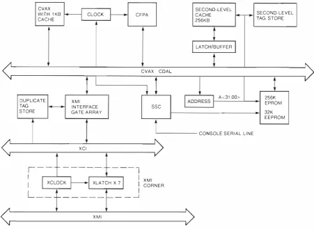
Al l VAX 6200 X M I mod u les i nterface to the XMI throug h a set of eight semicustom pans. These eight c h i ps a re p hysical l y mounted on a section of the modu l e known as t he "XMJ cor ner " This section of the mod u l e is approximately
1 2 . 7 em ( 5 i nches) by 3 em ( 1 . 2 i nc hes) and is
located by t he A, B , and C connectors of t he mod u l e . (See Figu re 2 . ) The X M I i nterface area is identical on all modu les so that a common e l ec trical load is presented to a l l s lots on the X M L The X M I corner h a s four 4 4 -p i n cerquad pack ages on side 1 of the modu l e and four 4 4 -pin cerquad packages on side 2. I n addi t ion, approxi mately 1 00 surface-mounted-device (SMD) sig nal termi nation resistors and bulk power capaci tors are d ivided eve n ly across both sides of the mod u l e i n the X M I corner.
Figure 2 is a photograph of the three VAX 6 2 0 0 X M I modu les . Note t h a t a l l t hree modu les have the identical components i n t he lower right cor ner and a s i m i lar gate array d i rectly above the XMl corner.
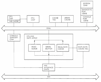
VAX 6200 CPU Module
As noted earl ier, t he VAX 6 2 0 0 CPU ( KA6 2A) is based on the C MOS VAX chip known as the CVAX . The KA6 2A is a s i ngle modu le that i mp lements a fu l l CPU subsystem . I nc luded on the KA62A mod u le are
• The CVAX c h i p , which includes a 1 k i l obyte ( KB) on-chip cache
• An external 2 5 6KB cache
• A floating point accelerator chip (CFPA)
• Console support hardware
• An i nterface to the X M I
Figure 3 shows a b lock d i agram of t he KA6 2A modul e .
C P U
C H I P
r--Figure 2 Three VAX 6200 Xll11 Modules
F P U CACHE 256 K B
C H I P TAG CAC H E
E E P ROM
3 2 K B
DIAGNOSTIC
ROM 1 28 K B
CONSOLE ROM
l K B CACHE 1 28 K B
CONSOLE
S U PPORT
C H I P
<
I
COALI
I
I
C P U / X M I GATE A R R AY
i
J
R EA D WR ITE INVALI DATE D U P L ICATE
Q U E U E B U F F E R Q U E U E CAC H E TAG
I
I
X M I I N T E R FACE
C H I P S
[image:15.594.69.518.86.309.2] [image:15.594.84.500.368.706.2]X M I
Figure 3 VA X 6200 CPU Module (KA 62A) Block Diagram
Digital Technical journal 13
A n Oueruiew of the VA X 6200 Famill' of Svstems
Usi ng the CVAX processor with an HO-ns cyc le t i me, the KA62A CPU mod u le performance is approxi mately 2 . 8 t i mes that of the VAX- 1 1 /780 system . For a rota I system performance up to I I t i mes greater than the VAX- I l j7 H O , u p to four KA(J2A CPU mod u l es may be configured in a VAX 6 2 0 0 syste m .
The KA6 2A CPU mod u l e contai ns a two- level cache to reduce memory access t i me . The pri mary cache is I KB i n size and resides inside the CVAX chi p . This cache contains onl y i nstruction data to e l i m i nate the need to i nva l idate this data as other processors write to cached data loca tions. (The VAX architectu re provides strict ru les for mod i fication of instruction type data . ) The secondary cache is 2 5 6KB in size a nd contains data as we ll as i nstmct ions . The KA62A moni tors write transact ions on t h<.: system i ntercon nect and in va lidates any cached locations wri tten by another CPU or 1/0 device.
8 - B I T B AN K 4 8 M B (64 B I T S x 1 M WORDS)
ECC
8-BIT BAN K 3 8 M B
(64 BITS x 1 M WORDS)
ECC
8 - B I T
BANK 2 8 M B ( 6 4 B I T S x 1 M WORDS)
ECC
8 - B IT
BA N K 1 8 M B (64 B I T S x 1 M ,WORDS)
ECC
M EMORY CONTROLLER
GATE ARRAY
l
l
1 6- EN T R Y 8 - E N T R Y DATA
LOCK TA B L E C O M M A N D Q U E U E
Q U E U E
l
J
X M I I N T E R FACE
C H I PS
[image:16.597.74.290.365.698.2]X M I
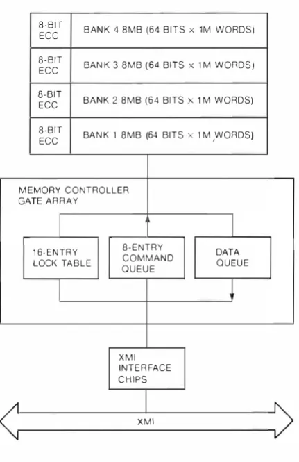
Figure 4 VAX 6200 Memory Module (M562A ) Hlock Diagram
14
Memory
The VAX 6 2 00 me mory subsystem is made up of memory control ler ;array modu les and is k nown as the MS62A . The MS6 2A modu l e , shown i n Figure 4 , conta ins a memory cont rol ler c h i p a nd � 2 megabytes ( MB) of ! - megabit ( Mb) dyna m ic RAMs ( D RAMs) . The MS62A maintains a 64 -bit data path between the memory com rollcr c h i p and t he RAMs, and i mplements an 8-bit error-cor recti ng code ( ECC) for each 64-bit word . The MS6 2A con ta i ns hardware to i mplement up to 1 6 " l ockable" me mory l ocations per memory array . These memory locks are used extensively by pro cessors and I/0 devices to ensure s i ngu lar access to data structu res i n a shared-memory m u ltipro cessor system .
The greater memory bandwidth req u i red by m u l t i p le processors and I/0 channels is achieved by memory i nterl eavi ng. The MS62A a llows inter leaving on 3 2-bytc bou ndaries. As l ong as mem ory add resses are randomly distributed across the lower 6 address bits, the bandwidth of the total memory su bsystem can be i ncreased l inearly with the addition of i n terleaved memory controllers.
The MS62A memory modu les may be i n ter l eaved two, fou r, or eight ways. The i nterleave factor is automatica l l y determined by t he system u pon power-up or system i n i tiali za tion . How ever, designers have given the user the a b i l i ty to manually specify t he i n terleave c haracterist ics of the me mory subsyste m . Up to eight MS62A mem ory modu les may be configured in a VAX 6 2 00 systl' m .
IjO Channels
The VA,'\ 6 200 system uses t he VAXB I bus as the i nterconnect for a l l 1/0 devices. The system i nterface to the VAXB I is a rwo-modu le set cal led the DWMBA. Figure 'S shows a block d i agram of the DWMBA mod u l es. The DWMBA/A module is connected ro the XMl , a nd the DWMBA/B mod u le is connected to t he VAXBI . These two modu les arc in terconnected with a 1 20-wire cable assem bly which may be up ro 4 . 6 meters ( I 5 feet) long.
Thl' DWMBA al lows VAXB I devices to read sys tem memory at up to 'S . SMB per second and ro writl' system memory a t up to 1 3 . 3 MB per sec om! . Any VAX B I-compatible device may be con nected to the VAX 6 2 0 0 systems t hrough t he DWM BA. Al l VAX 6 2 0 0 systems contai n a m i n i m u m o f two VAXBI channels and m ay option a l ly conta in up ro six VAXBI channels.
Digital Technical journal
System Interconnect, the XMI
The X M I . t h e p r i m a ry e l ectrical int erconnect i n t h e VAX 6 2 0 0 fa m i l y o f computer systems. en com passes
• The protocol obse rved hy a node on the X M I
• The e l ectrica l e n v i ronment o f t he XM l
• The backpl ane
• The logic used to i m plement th e protocol
The X M I can support m u l t i ple processors. mu l t i p l e me mory s u bsyste ms. and m u l t i p l e 1 /0 channel adapters .
X M l nodes may be c l assi fied as commanders or responders. dependi n g on their role in a given t ransact ion . A commander is a node that is i n i t iar i ng an XM I r ransact ion . A responder is the node that must act u pon the t ransaction . A processor node usua lly acts as a com mander. ( Howeve r. a processor node may become a responder i f anot her node reads a con t rol/status re gister on the CPU .) Memory nodes. on the other hand. arc a l wavs responders si nce they cannot i n i t iate an
Xl'vl l t ransact ion . 1 / 0 nodes may act as e i t her com manders or responders. depend i n g on the type of 1/0 operation . The fu nctions of these nodes arc furt her expla ined in sec tions below .
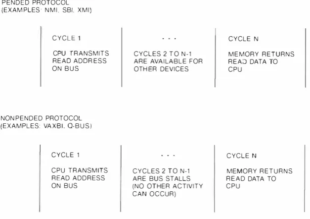
Beca use the Xi\H is a pcnded in terconnect . sev era l tra nsact ions can be in progress s i m u l ta neous l y . When an X M I com mander i ni t i a tes a req uest for a read or to sol icit an i nterrupt vector. an identifier code is a l so transm i t ted to the sc::l ccted responder. At t h i s po i nt . contro l of the
X l'vtl is re l i n qu ished. and ot her transact ions arc a l l owed to take p lace whi lc the responder fe tches the req uested read data or i nt e rrupt vccror. The responder the n arb i t rates for con trol of the XM I
and re t u rns the requested data or vector a l ong with t he ident i fier code . By mon i toring the ident i fier codes. t he i n i t i a l commander is abk ro
receive t he correct data and conti n u e .
Arbi trat ion and data transfers occur s i mu l ta neously over a m u l t ip l e xe d set of address and data l i nes. and a se pa rate set of arbitration l i nes. The XM I supports quadword . octaword . and hex word reads to memory. as we l l as quadworcl a nd ocraword me mory writes. I n a d d i t i on . the XM I su pports longword - l engrh read a nd write opera t ions ro l /0 spa c e . These l ong word operations
i m p l ement byte and word modes req u i red by cer tain l/0 devices
Digital Technical journal
.\'o. - ,-J. ugus/ I '.IHH
The XMl has :)0 address h i ts. and t he s m a l l est addressa ble entity is a s i n g l e b)'l e . XM 1 address space is d iv ided intO two halves by b i t 29 of t he address . When bit 29 equals zero . an address is sai d to fa l l i n to memory space . When b i t
2 9 equals one . the address is sa id to fa l l w i t h i n l /0 space . T h i s arra ngement marches t he m a x i mu m p hysica l address a s defined b y t he VAX
arc h itec ture and a l l ows up to ') 1 2MB of p hysical memory ro be addressed . The XM l arc h i t ectu ra l l y a l l ows up to 1 6 nodes, but is physica l l y a nd e lcc trica lly constra i ned ro 1 4 nodes.
VAX B I
B I IC
VAX B I VA X B I MODULE I N T E R FACE
GATE A R R AY
I B U S
T R A N SC E I V E R S
�
� B U S CABCEU P TO 15 FEET I N LENGTH
I B U S
T R A N S C E I V E R S
X M I X M I
MODULE I N T E R FACE GATE A R R AY
X M I
I N T E R FACE
C H I PS
[image:17.596.291.515.256.709.2]X M I
Figure 5 VAX 6200 VAXRI Chan n el Adapter Rlock Diagra m
--- A n Overview of the VA X 6200 Fami�y of Systems
The XMI multi plexes data and address i n forma tion onto the 64 -bir data pat h . Data transactions arc i n i t i ated with a " command and address" cycle, fol l owed by mu l ti ple data cycles . The max i mum length for an XMI tra nsact ion i s 3 2 bytes of data . The X M I cycle r i me is 64 ns. The effective band wid th of the XMI is a fu nction of the data transfer size , as shown in Ta ble 2 .
The X M l arc hi tecture allows for three d isti nct c lasses of devices .
Processor Nodes
Each processor node conta i ns a C PU that e xe cu tes i nstruc tions and manipulates data con ra i ned in X M I me mory. The processor node can execute any i nstruction set com pati ble with the VAX-sry le byte address i ng and memory l oc k i ng mechan isms . A processor node will have a cache t hat must force all written data back to main memory. Any cached processor module must a lso monitor write traffic on the XMI a nd i nval idate any l ocation i n i ts own cache that is written i n to main me mory. Processor nodes must a l so be capable of responding to interrupt req uests gen erated ei ther b y other processors o r b y ljO nodes .
IjO Nodes
I jO nodes genera l l y respond ro I/0 space refer ences e ither by mapping the data onro another bus or by in terpret i ng data as a command . An
I/0 node can a l so become a commander on the XMI and access global XMI memory. ljO nodes may generate i n terrupt sequences d i rected toward processor nodes. However, I jO nodes do nor respond to com mands directed toward me m ory space .
Memory Nodes
Memory nodes act only as responders on the XMI . They respond to read and write requests d i rected toward memory address space . These requests are generated either by processor or 1/0 nodes .
Data In tegrity
The X M I contains a n u m ber of features to en ha nce the i ntegrity and reliabi l i ty of the intercon nect. Fi rst, a l l X M I information transfer l i nes arc parity protected, and X M I com mand confirmation signals are ECC protected . The X M I protocol i s suffic iently robust t O permi t detection and recovery of all si ngle-bit error cond i tions on these signa ls. Add i t ionally, the XMI defines t i me
1 6
Table 2 XMI Bandwidth Based on Transaction Size
Transaction Interconnect
Size in Bandwidth
Bytes in MBjsecond
4 3 1 .25
8 62.50
1 6 83.33
32 1 00.00
our condi tions that may be used to detect and d iagnose fai l ures .
VAX
Console
The VAX 6 2 0 0 system implements the standard VAX console fu nctionality by means of software that condi tionall y exec utes on each of the KA6 2A CPU modules . Each KA6 2A C PU module contains a serial-line i n terface, 2 5 6MB of read-only mem ory (ROM ) , 3 2 MB of electronically erasable ROM (EEROM) , and 5 1 2 bytes of RAM . Control is passed to the console software upon any one of the followi ng occurrences:
• System power-up
• I n i ti a l i zation
• Receipt of a controi - P character from t he con sole ter m i nal
• Execution of t h e HALT i nstru ction
• Some severe error condi tions
Each KA6 2A CPU has access to console termi nal transmi t-and-receive l i nes carried on the sys tem backplane . Upon power-up, control of the system console term inal is dyn a m icall y a llocated to one of the CPUs prese n t in t he syste m . This CPU , known as the " boot" processor, provides t he system i n terface ro t he console terminal as we ll as ro the swi tches and l i ghts located on the system control panel .
On receiving comm ands from the console ter m i na l , t he boor processor may run d iagnostics or boot an operating syste m . This processor commu n icates w i t h other processors by means of a struc ture maintai ned in me mory known as the console commu n ications area (CCA ) .
Also considered as part of the console sub system. a T K '5 0 tape drive is incl uded in each VAX 620 0 syste m . The tape drive is connected to the system hy means of a TBK '5 0 controller mod uk located on a VAXBI l/0 channe l and is used for the fol l ow ing pu rposes:
• Saving a l l volati l e parameters for the console
subsystem
• Loading t he VA,'( Diagnostic Su pervisor (VDS)
when no d isk is avai !able or functiona l in the system
• Distri buting operating system and layered soft ware
The TK'50 tape drive is a lso ava ilable under oper ating system con trol as a general - purpose data
i n terc hange device .
Built-in Self-test
Extensive bu i lt-in sel f-test is used by al l modu les contained within the VAX 6 2 00 systems. Upon power- u p . a l l mod u l es within the syste m , with the except ion of the DWMBA, perform a se l f-test in para I l e t . After self-test is com plete, t he CPU modules exa m i ne each other's status; the one i n t h e lowest slot nu mber that passed self-test is selected as r he boor processor. The boot proces sor then continues to execute an addi t ional test
ro ensure memory accessibi l i ty and fina l l y exe
cutes a tesr of the DWMBA.
Physical Packaging
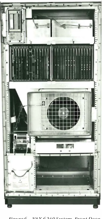
Al l VAX (J 200 systems are housed i n the same cabinet, which is 7R em (30 '5 i nches) wide by I 54 em ( 6 0 . "i inches) ta l l by 76 em ( 3 0 inches) deep. The cabinet contains one 1 4 -slot XMI back plane , two (J -slot VAXBl backplanes, and all nec essary power and cool i ng to sustain a wide range of configurations Figure 6 shows a VAX 6 2 4 0 with the front door removed.
The XMI is physica l ly implemented in a 1 4 -s lot backplane assembly contai ning Z I F mod
u l e connectors. signa l terminating networks, and
a centra lized c lock and arbitration system . Mod
u l es are located on 2 em ( 0 . 8 i nc h ) centers . The Xi\'1 1 bac kplane is supp l ied wi th + 5 volts (V) for ge neral logic. a separate + 5 V supply for mem ory. ± 1 2 V for t be console term inal l ine drivers, and -'5 2 V 1 - 2 V for em itter-coupled logic ( FC L ) . Presen t l y none of the VAX 6 2 0 0 XMI mod u l es uti l izes the ECL voltages . but ECL is incl uded for poten tial fut u re usc .
Digilal Technical journal No. 7 A ugust 1')88
Figure 6 VA X 624 0 System, Front Door Removed
The VAX 6 2 0 0 systems a l l contain two 6-slot VAX BI backplanes, which arc configured as i nde pendent channe l s . The first slot of each VAX BI backplane is occupied by the DWMBA/B modu le, leavi ng '5 sl ors for standard VAXBI i ntcrfaces . Al l systems conta in a DEBN K T K '5 0 tape control ler and a DEfiNA Et hernet control ler as standard equ i pment. The rwo VAX BI backplanes are sup p l ied with + 5 V, ± 1 2 V, - '5 . 2 V, and - 2 V.
Summary
The VAX 6 2 00 fam i ly of systems merges the CMOS VLSI VAX c h i p , which is used in a number of Digi ta l 's prod ucts, with a very high
[image:19.596.304.507.83.517.2]--- A n Ot,ervieu• of the VAX 6200 Family of Svstems
mane<:: memory and 1/0 subsystem . Th is hard ware. combined with the new fu l l y symmetric mu l t i processi ng capabi l i t ies of VMS version 5 . 0 , a llows very high system t h roughput previously achievable onl y with ECL technology. Moreover. the extensive usc of CMOS tec hnology res u l ts in p hysical ly smaller systems. These sma l l e r sys tems consume less power and are more re li able due 10 the lower component cou nr and lower power consu mpt ion .
1 8
References
I . P Wade. "The VAXB1 Bus - A Random l y Configurable Design," Digital Technical journal (February 1 987) : 8 1 -8 7 .
2 . T Fox . P . Gronows k i . A. Ja i n , B . Leary, a n d D . Miner, "The CVAX 7 8 0 3 4 Chip, a 3 2 -bit Second-genera tion VAX Microprocessor , "
Digital Techn ical journal (August 1 9 88. this issue) : 9 5 - 1 08 .
Digital Technical journal
The Architectural Definition Process
of the VAX 6200 Family
The architectural definition of Digital's VAX 6200 family was governed by a twofold goal: to build a system with higher throughput than previous CMOS, Q-bus-based systems at a cost lower than ECL-based systems. Deci sions made during the definition process were influenced by firm schedule guidelines. Further, the very nature of the multiple processor system imposed its own requirements, particularly in the definition of the XMI bus. This new 64-bit-wide interconnect is specifically designed to meet the memory and I jO needs of the symmetric multiprocessor system. Through out the architectural definition process, engineers continually evaluated the interdependency of one design decision upon another and against the project and schedule goals. By this process, the total definition of the sys
tem - the XMI bus, the processor module, memory module, console sub system, and packaging - was achieved.
Defin i t ion of the VAX 62 00 fam i l y of systems began in Marc h 1 98 '5 . The engi neers' i n tent was tO design a fol low-on p rod uct w the VAX 8 2 00/ 8:) 0 0 fa mi l y of syste ms. st i l l in deve lopment at that t i me . This paper d iscusses t he system arc h i tectural de fi n i t ion process t hat took place during
1 98 '5
Li ke t h e VAX 82 00/8 300 fam i ly before i t , t he VAX 6200 fa m i ly provides a system environment for a VLSI VAX c h i p set . This new fam i ly of sys tems is a mid-range VAX i m plementation . In t h i s context. a m id -range syst em i s defi ned as a pro duct w i t h more capabi l ity t h a n t h e Q-bus-based systems and less capabi l i ty than the e m itter-cou pled logic (ECL) based systems.
Project Goals
The pri mary goa l of the VAX 6 2 0 0 program was twofold: to b u i l d a system w i t h greater system t hroughput t han the CMOS . Q-bus-based VAX sys tems , and to ensure system cost was lower than that of high-performance EC L- based systems. Desi gners wou l d achieve this goa l by design ing a system arc hi tecture t hat al lows a moderate num ber of low cost CMOS VAX m icroprocessors to sh are a com mon system env i ron men t. Such an efficient m u l t i processor system envi ronment wou ld offer h i gher throughput for a large n u m b e r o f appl icat ions a n d a t a cost lower t han a h i gh -performance single processor.
Digital Technical ]om-r1al No. 7 A ugust I 'J88
Once the decision tO bu i l d a m u l t iprocessor was made . the next q uestion was how many processors to i nc l ude. Several sma l l computer manufacturers were bui l d i ng 8- to 3 2 -processor systems at the t i me. Our bel ief was that t he mar ket for systems w i t h n u merous processors was fa i rly sma l l because few appl icat i ons wou l d run effic iently on t hese syste ms. Therefore, we dec ided ro design the VAX 6 2 00 as a 4 -processor system . w i t h t he possi b i l i ty of expansion to 8 processors . This arrangement wou ld a l l ow us to sri 11 configure cost-effective 1 -ro 2-processor sys tems. If we found a signi ficant nu mber of appl ica ti ons cou ld benefit from the larger n u mber of processors, we cou ld expand to 8 processors.
Bui l d i ng an efficient m u l t i processor system wou ld necess i tate opt i m i zat ion of both hardware and software funct ionali ty . The VMS asym met ric mu l t i processi ng code (VMS versions 2 through -4 ) that supported t he VAX- I l j7 8 2 , VAX 8300, and VAX 8800 systems worked we l l for compute bound , d u a l -processor systems. However, asym metric operating system software wou ld not be accepta ble for larger sca le mult i processors. In the exist i n g VMS asymmetric m u l t i processi ng design . most operating system code was exe cuted on t he processor designated as t he " pr i mary" processor. Whenever a process needed to perform ljO or i nvoke most of the VMS system serv ices. the process wou l d have to be schedu led
--- The A rchitect ural Definitio n Process of the VA X 6200 Fa mily
on the primary processor. The task of m a k i ng VMS more symmetric in i ts handl i ng of !jO and VMS system services was undertaken ro su pport t he VAX 884 0 and the VAX 6 2 0 0 fam i lies. 1
Discussion of how \ve chose to opt i mi z e the VAX 6 2 0 0 hardware begins i n the sect ion The System I n terconnect.
Schedule
In March l l)H') the des i gn of the CVAX c h i ps was a l n:ady wel l u nder way . These chips wou ld be del i vered in t i me to a.l low systems to s h i p in late I 987 Based on the CVAX c h i p set schedu l e , we esta b l ished the fol low i ng schedu le for the devel opment of the VAX 6 2 0 0 system :
Six mon ths of arc h itectural defi ni tion
Twelve months of designjsimulation
Three months to budd and test approxi mately five fi rst-pass prototypes
Six mon ths to b u i l d approxi mately 70 second pass protOtypes
Three months for final test i ng and manufactur ing i ntrod ucrion
This two and a ha lf year schedu l e s i g n ificantly i n fluenced the defi n i ti on of the system archi tec tu r<.' as we l l as the se lection of i m plementation technologies . (Actual i m p lememarion rook three years . The design/si mulat ion p hase took three months longer rhan expected , a nd rhe fi rsr-pass prototype phase rook th ree months longer than expected )
The System Interconnect
The first order of business was to define a new sys tem i nterconnect. This i nterconnect wou l d have rhe bandwidth requ i red tO su pport the memory ancl 1/0 needs of the mul t i p l e processors We ou t l i ned three requ i rements that wou ld affect the design of t he new system i n tercon nect.
• We esti mated that each CVAX processor wou ld
req u i re between 3 megabytes ( M B) and 6 M l3 per second of dara tojfrom memory. This rare wou l d depend on the c l ock rate of the pro cessor, the selected cache arc h itecture , and the cache " hi t " rate of t he program being executed .
• We also esti mated that each processor cou ld req u i re peaks of 1 M B ro 1 . 5 M B per second of l /0 bandwidth.
20
• To maint a i n predictable memory access t i me ,
we decided that the system bus shou ld not be run over 7 '5 percent u t i l i zed .
Usi n g the worst- case amici pared bandwidth needs, 80MB per second of peak bus bandwidth would be req u i red to su pport 8 processors .
fkcause of t he tight schedule and our aware ness of the sign i ficant a mou n t of t i me needed to design a new system bus, we first looked i nto the feasi bi l i ty of using an existing bus. We consid ered hut rejected the existing VAXB I bus, the primary in tercon nect for the VAX 8 2 00/83 0 0 syst e m , because o f i ts l i m i ted 1 3 3 MB p e r second bandwidt h . We a lso rejected the N M I bus, the VAX 8 '5 0 0j8700j8 800 fa m i ly i n terconnect , beca use t h is bus uses ECL techno logy. At one point we even considered using the SBI from the VAX - I 1 /780 system w i t h a 6 4 - b i t data path i nstead of i ts exist i ng 3 2 - b i t data pat h . After extensive ana lysis , however, we decided a new system bus wou ld have w be engi neered for the prod uct to meet i ts goal s .
Al though we wou ld have ro define a new bus for processor-to- memory commu nications, the sched u l e did not a l low us to design a fu l l com p le rnenr of IjO i nte rfaces for the new bus. Si nce a large n umber of !jO i nterfaces woul d be ava i l able on t he VAXBI , the des ign team decided to
use the VAXBJ as the i nterconnect to a ll IjO devices. The new system i ntercon nect , the X M I , woul d be used only t o connect processors, mem ories, and VAXBI c hanne l ada pters . Therefore , i n addi t ion to the req u i rements l isted above , the X M I archi tectu re wou l d a lso al low multiple VA.,'\ B I channe l adapters to opt i m i z e 1/0 through put where necessary for large systems. Use of the VA.,'\BI for l/0 adapters also had the pos i t i ve effect of m i n i m i z i n g the n u m ber of e l ectrical i nterconnects tO the X M I ; the phys ical length of the X M I wou ld consequently be shorter and the tOta l capaci tance lower. Further discussion of the channel adapters is presented in the section VAXnt Channel Ad apters .
I n June 1 9 8'5 a tea m o f l l sen ior- level engi neers was assembled ro prod uce the arc h itectu ra l and e lectrical speci fication for t h e X M I b u s and the VAX 6 2 0 0 system . In addit ion to arc h itectu ral a nd e lectrical experts, this team i nc l u ded one represe ntative from each of the anticipated mod u l e design reams. Almost a l l members had prev i ously worked o n projects i nvolving the VAXBI bus. It was understood that the XMI woul d be
Digital Technical ]oun�al
used solely for the VAX 6 2 0 0 fam i ly of systems, un l i ke the VA.-'\ 13 1 . which would be used across many different appl ications. A strict adherence to this prem ise great l y he l ped the speci fication team to put tech n ical trade-offs i n perspective .
XMI Electrical In terface Definitio n
Since most of the VAX 6 2 0 0 system is CMOS and transistOr-transistor logic (lTL) based, we i m me diately decided th<: XMl could not be i mpl<: mentecl i n ECL To maintain a TIL- level bus and to ach ieve the desi red bandw idt h , the data path c learly wou ld have to he 64 bits wide . Further. to meet our goal of 80MB per second bandwidth, the XMf wou ld have to transfer 6 4 bits of infor mation every 80 nanoseconds (ns) . (Th is transfer rate assumes a protocol i n which address and data arc multi plexed. and up to 3 2 bytes of data can he transferred per address cyc l e . )
Several e lectrical alternatives were considered for t he X M I . A scheme using the com mercial ly ava i lable FumreBus components was seriously cons idered . However. we rejected this scheme because a large nu mber of components wou ld be necessary to implement the 64 -bit data pat h .
The lack of commercially avai lable compo nents to drive a 64 -hit bus at the requ i red speed tinally led us to a decision . We wou l d design a hit-sl iced custom CMOS bus interface chip set. Each chip wou ld transce ive 1 1 J i nes, and seven chips would be used for the entire data pat h . Al though t h e "sl iced " bus interface wou ld use more module real estate than a l a rger c h i p , the s liced bus design greatly simpl ified the c h i p packaging problems. Each chip wou l d fit into a standard 4 4 -p i n cerguad package . A sliced X M I interface also allows each c h i p t o dissipate under 0 . '5 watt ( W ) , which enhances rel iabil ity and rel ieves the need for heat sinks on the part . Wi th out hear s i n ks . the XMI i nterface parts can be
mounted on both sides of each mod u le. This arrangement saves '50 percen t of the real estate necessary to i nterface to the X M I .
To si mpl ify rhe design of t he fu ll cusrom X M I interface parts, we wou ld keep the functional req u i rements for rhe pans as si mple as possible. The XMI i nterface chips have l ittle knowledge of the X M I protocol and serve only as the electrical i nterface . Due to the divergent needs of pro cessor, memory, and 1/0 interfaces, desi gners already knew that each mod u l e woul d need a different VLSI chip for X M l i nterface funct ions . We decided, therefore , that each modu le VLSI
Digital Technical journal No . 7 A ugust I 'JRR
chip wou ld he requ i red to supply the logic ro i m p le ment r he bus- l evel protocol .
As the electrical des ign of the XMI progressed, a bus cyc l<: as fast as 64 ns appeared feasible. Al though not entirely necessary ro su pport the stared system pe rformance goa ls, the faster XMI cycle time was strongly pursued to ga i n extra margi n in the system design . Furthermore , this fast cycle t i me wou ld a llow the poss i b i l ity of sys tem upgrades ro faster processors in rh<: future . Consequently, 6 4 ns became the stared goal for the X M l cycle t i me; 80 ns was rhe fa l l back strat egy if the design complexity of a 64 -ns cycle rime began ro place the overa l l project schedule ar risk.
Logic design across the entire system was done assum ing a 64 -ns cycle rime . Eventua l l y 64 ns became the actual speed of rhe bus as the CMOS process was characterized and rhe fi rst parts were sampled and found to contain sufficient margi n to support rhe faster cycl e t i me.
XMI Protocol Defin itio n
X M I prorocol defi nition took place i n para llel with rhe electrica l defi n i t ion of the bus . It was clear from the start that the bus wou ld cycle sev eral times faster than the memory subsystem . This difference in cyc l e t i mes i mmediately led us to the decision rhar the X M I wou ld ru n a " pended " bus protocol . A pended bus protocol a l lows con trol of the X M I tO be re linquished between a "read" com mand and the return of rhe data from the memory su bsyste m . With mul tiple processors and multi ple memory control lers , seve ra l read commands could be outstandi ng at a rime.
To opti m i ze data traffic on the XMI bus, we needed ro defi ne data transfer com mands of several l e ngths . Since VAX i nstructions may write as l ittle as I byte of data, a 64 -bit write command was defined . (There is a mask field associ ated with the write command that allows single bytes to be wri tten . ) Si nce the VAXBI bus already had commands to transfer 1 6 bytes of clara per address , it was essential to al low simi lar commands on the X M I bus to m i n i mize the in terface complexities r o t h e VAXB I . Eventual ly we added a 3 2-byte read command tO a l l ow processors ro prefetch larger amounts of data upon cache m isses. A _3 2 -byte wri te command was not i m p l e mented, because it wou ld be roo great a bu rden for t he memory controller ro buffer multiple 3 2 -byte write commands .