A Study on Transimpedance Amplifier in 0.35 µm CMOS
Technology
Davender Singh
Department of Applied Physics Guru Jambeshwar University of
Science & Technology, Hisar, India
Ajay Shankar
Department of Applied Physics Guru Jambeshwar University of
Science & Technology, Hisar, Indja
Manoj Kumar
Department of Electronics andCommunication Guru Jambeshwar University of
Science & Technology, Hisar, India
ABSTRACT
This paper presents a design of the transimpedance amplifier using 0.35µm CMOS technology. In the proposed transimpedance amplifier, feedback resistor RF of conventional transimpedance amplifier has been replaced by NMOS transistor as an active feedback resistor. This circuit operates at 3.3V power supply voltage and for a photocurrent of 0.5µA.The proposed transimpedance amplifier having low noise, high gain and large dynamic range. The simulated results of transimpedance gain in single stage and three stage transimpedance amplifiers is 4.43 MΩ and 4.39 MΩ at gate voltage of 0.4V. Power dissipation of single stage and three stage transimpedance amplifier is 602.04 µW and 1.781mW at gate voltage of 2.0V.
Keywords
Transimpedance amplifier, CMOS technology, low noise amplifier, optical receive, negative feedback
.
1.
INTRODUCTON
A transimpedance amplifier (TIA) is a circuit that converts a current signal into output voltage signal whose voltage is dependent on magnitude of current. The demand of higher data rates transportation over the internet and multimedia communication in recent years result in fast development of high speed optical communication system. Transimpedance amplifiers are very useful circuit components in optical communication system. Front-end of transimpedance amplifier (TIA) is one of most critical building block at electro optical interface on receiver side, which determines the performance of whole system to a large extent, such as speed, gain, sensitivity and noise etc. The performance of optical interconnection system depends on receiver gain, bandwidth, noise and power consumption. Silicon-based CMOS technology [1] is the only candidate which can achieve the required level of integration with reasonable speed, gain, cost, power consumption.
[image:1.595.323.536.216.343.2]The transimpedance amplifier [2] uses a closed loop circuits as shown in figure 1. This circuit allows not only to avoid the problem of the dynamic range, but also to obtain a trade-off between the high and low impedance configuration. It is relatively high bandwidth and dynamic range as well as a good noise level.
Figure 1: Block diagram of transimpedance amplifier used in an optical receiver
The bandwidth can be improved by increasing the open loop gain of amplifier, whereas when transmission speed is increased, the number of stages composing the amplifier [3] as well as its open loop gain is necessarily reduced. In this paper, transimpedance amplifier parameters such as transimpedance gain, power consumption and output voltage are studied in 0.35µm CMOS technology.
2.
CIRCUIT DISCRIPTION
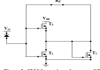
Figure 2 shows CMOS transimpedance amplifier circuit used a push-pull inverter at the input to maximize the transconduction of amplifier [4] and increases its gain bandwidth product (GBP).
Figure 2: CMOS transimpedance amplifier
[image:1.595.339.503.527.643.2]The expression of gain for transimpedance amplifier will be:
(1)
where: gm1, gm2, gm3 = transconduction of T1, T2, T3 transistor,
Another expression of gain for transimpedance amplifier
given by:
(2)
where:
(3)
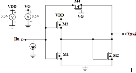
2.1 Proposed Single Stage Transimpedance Amplifier
[image:2.595.53.275.75.263.2]
Proposed single stage transimpedance amplifier consists of three NMOS transistor and one PMOS transistor. A photocurrent of 0.5µA is used in the circuit. In proposed single stage TIA circuit feedback resistor RF is replaced with NMOS transistor as an active feedback resistor biased by the gate voltage VG. There is a voltage source Vdd of 3.3V which is applied to each PMOS transistor. NMOS transistor having width of 1.0µm and length 0.35µm is used in the circuit as shown in figure 3. Amplification of signal occurs from input to output. In TIA output is taken at terminal Vout, and a portion of output given feedback to the input of the amplifier.
Figure 3: Proposed single stage CMOS transimpedance amplifier
2.2 Proposed Three Stages Transimpedance Amplifier
Three stages transimpedance amplifier consist of three identical cascaded stages having seven NMOS transistor and three PMOS transistor. A photocurrent of 0.5µA is used in the circuit. In proposed three stages TIA circuit feedback resistor RF is replaced with NMOS transistor as an active feedback resistor biased by the gate voltage VG. There is a voltage source of VDD of 3.3V which is applied to each PMOS transistor. NMOS transistor having width of 1µm and length of 0.35µm and PMOS transistor having width of 2µm and length 0.35µm used in the circuit as shown in figure 4.
The feedback resistor will be determined using
(4)
where W =width, L = length, VGS = gate to source voltage, VT = threshold voltage
Figure 4: Proposed three stages CMOS transimpedance amplifier
The bandwidth of transimpedance amplifier is approximately equal to:
(5)
The stability of the system is related to A, and total gain of the system must be controlled. This is given by
(6) Where A0 is the open loop gain of the single stage
3. RESULTS AND DISCUSSION
3.1 Single Stage TIA
Table 1 shows output voltage, power consumption, transimpedance gain level with varying the magnitude of gate voltage VG [0.4 – 2.0] V for single stage TIA [Figure 3]. Power consumption varies from [955.21 – 602.40] µW with the variation in magnitude of gate voltage VG from [0.4 – 2.0] V as shown in figure 6. Output voltage varies from [2.21 – 1.36] V with the variation in magnitude of gate voltage VG from [0.4 – 2.0] V as shown in figure 5. Transimpedance gain varies from [4.43 – 2.73] MΩ with the variation in magnitude of gate voltage VG from [0.4 – 2.0] V as shown in figure 7.
Table -1: Variation of power and transimpedance gain with gate voltage
Gate voltage VG (V)
Power
consumption (µW)
Output voltage Vout (V)
Transimpedance gain (MΩ)
0.4 955.21 2.2192 4.438
0.8 911.01 2.1537 4.307
1.2 843.07 2.0556 4.111
1.6 743.71 1.8004 3.600
[image:2.595.55.275.429.548.2]Figure 5: Variation of output voltage of single stage TIA with gate voltage
Figure 6: Variation of power of single stage TIA with gate voltage
Figure 7: Variation of transimpedance gain of single stage TIA with gate voltage
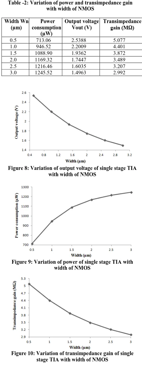
Table 2 shows output voltage, power consumption, transimpedance gain level with varying the width of NMOS transistor [0.5 – 3.0] µm for single stage TIA [Figure 3]. Power consumption varies from [713.06 – 1245.52] µW with the variation in the width of NMOS transistor from [0.5 – 3.0] µm as shown in figure 9. Output voltage varies from [2.53 – 1.49] V with the variation in the width of NMOS transistor from [0.5 – 3.0] µm as shown in figure 8. Transimpedance gain varies from [5.07 – 2.99] MΩ with the variation in the width of NMOS transistor from [0.5 – 3.0] µm as shown in figure 10.
Table -2: Variation of power and transimpedance gain with width of NMOS
Width Wn (µm)
Power
consumption (µW)
Output voltage Vout (V)
Transimpedance gain (MΩ)
0.5 713.06 2.5388 5.077
1.0 946.52 2.2009 4.401
1.5 1088.90 1.9362 3.872
2.0 1169.32 1.7447 3.489
2.5 1216.46 1.6035 3.207
3.0 1245.52 1.4963 2.992
[image:3.595.307.545.73.692.2]Figure 8: Variation of output voltage of single stage TIA with width of NMOS
Figure 9: Variation of power of single stage TIA with width of NMOS
[image:3.595.323.533.443.653.2]Table 3 shows output voltage, power consumption, transimpedance gain level with varying the width of PMOS transistor [1.0 – 3.0] µm for single stage TIA [Figure 3]. Power consumption varies from [576.32 – 1159.82] µW with the variation in the width of PMOS transistor from [1.0 – 3.0] µm as shown in figure 12. Output voltage varies from [1.70 – 2.47] V with the variation in the width of PMOS transistor from [1.0 – 3.0] µm as shown in figure 11. Transimpedance gain varies from [3.40– 4.95] MΩ with the variation in the width of PMOS transistor from [1.0 – 3.0] µm as shown in figure 13.
Table -3: Variation of power and transimpedance gain with width of PMOS
Width Wp (µm)
Power
consumption (µW)
Output voltage Vout (V)
Transimpedance gain(MΩ)
1.0 576.32 1.7021 3.404
1.4 750.10 1.9411 3.882
1.8 888.37 2.1249 4.249
2.2 998.54 2.2684 4.538
2.6 1087.31 2.3825 4.765
3.0 1159.82 2.4750 4.950
Figure 11: Variation of output voltage of single stage TIA with width of PMOS
[image:4.595.325.534.73.199.2]Figure 12: Variation of Power of single stage TIA with width of PMOS
Figure 13: Variation of transimpedance gain of single stage TIA with width of PMOS
3.2 Three Stage TIA
[image:4.595.54.279.222.472.2]Table 4 shows output voltage, power consumption, transimpedance gain level with varying the magnitude of gate voltage VG [0.4 – 2.0] V for three stage TIA [Figure 4]. Power consumption varies from [1986.0 – 1781.0] µW with the variation in magnitude of gate voltage VG from [0.4 – 2.0] V as shown in figure 15. Output voltage varies from [2.19 – 1.55] V with the variation in magnitude of gate voltage VG from [0.4 – 2.0] V as shown in figure 14. Transimpedance gain varies from [4.39 – 3.11] MΩ with the variation in magnitude of gate voltage VG from [0.4 – 2.0] V as shown in figure 16.
Table -4: Variation of power and transimpedance gain with gate voltage
Gate voltage
VG (V)
Power consumption
(µW)
Output voltage Vout (V)
Transimpedanece gain (MΩ)
0.4 1986 2.1969 4.393
0.8 1966 2.1915 4.383
1.2 1937 2.1849 4.369
1.6 1945 1.1552 4.310
2.0 1781 1.5578 3.115
[image:4.595.324.553.403.676.2]Figure 15: Variation of Power of three stage TIA with gate voltage
Figure 16: Variation of transimpedance gain of three stage TIA with gate voltage
[image:5.595.70.268.236.352.2]Table 5 shows output voltage, power consumption, transimpedance gain level with varying the width of NMOS transistor [0.5 – 3.0] µm for three stage TIA [Figure 4]. Power consumption varies from [1432.0 – 2906.0] µW with the variation in the width of NMOS transistor from [0.5 – 3.0] µm as shown in figure 18. Output voltage varies from [2.54 – 1.46] V with the variation in the width of NMOS transistor from [0.5 – 3.0] µm as shown in figure 17. Transimpedance gain varies from [5.08 – 2.93] MΩ with the variation in the width of NMOS transistor from [0.5 – 3.0] µm as shown in figure 19.
Table -5: Variation of power and transimpedance gain with width of NMOS
Width Wn (µm)
Power
consumption (µW)
Output voltage Vout (V)
Transimpedance gain (MΩ)
0.5 1432 2.5427 5.085
1.0 1984 2.1944 4.388
1.5 2377 1.9180 3.836
2.0 2626 1.7195 3.439
2.5 2762 1.6010 3.202
3.0 2906 1.4688 2.937
Figure 17: Variation of output voltage of three stage TIA with width of NMOS
Figure 18: Variation of power of three stage TIA with width of NMOS
Figure 19: Variation of transimpedance gain of three stage TIA with width of NMOS
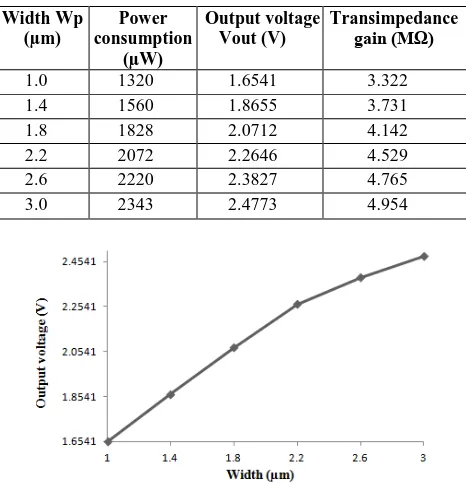
[image:5.595.329.529.251.373.2] [image:5.595.327.535.413.528.2]Table 6: Variation of power and transimpedance gain with width of PMOS
Width Wp (µm)
Power
consumption (µW)
Output voltage Vout (V)
Transimpedance gain (MΩ)
1.0 1320 1.6541 3.322
1.4 1560 1.8655 3.731
1.8 1828 2.0712 4.142
2.2 2072 2.2646 4.529
2.6 2220 2.3827 4.765
3.0 2343 2.4773 4.954
[image:6.595.61.295.106.704.2]Figure 20: Variation of output voltage of three stage TIA with width of PMOS
Figure 21: Variation of power of three stage TIA with width of PMOS
Figure 22: Variation of transimpedance gain of three stage TIA with width of PMOS
4.
CONCULSION
In this paper, the proposed transimpedance amplifier circuit present good performance in parameter such as
an active feedback resistor displays good optimized performance in terms of transimpedance gain, power consumption and output voltage. Transimpedance amplifier is better ability to operate in microampere range. Simulation result shows that transimpedance amplifier provides transimpedance gain in the range [2.73-4.56] MΩ by varying the biased gate voltage VG in the range [0.4-2.0] V.
5.
REFERENCES
[1] M. Nakamura, N. Ishihara, Y. Akazawa, and H. Kimura, “An instantaneous response CMOS optical receiver ic with wide dynamic range and extremely high sensitivity using feed forward auto-bias adjustment,” IEEE J. Solid- State Circuits, vol.30, pp. 991-995, September 1995. [2] M. Ingels, G. Vander Plas, J. Crols and M. Steyaert, “A
CMOS 18THz, 240Mb/s transimpedance amplifier and 155Mb/s LED driver for low cost optical fiber links,” IEEE J. Solid-State Circuits, vol.29, pp. 1552-1559, July1999.
[3] Escid Hammoudi and Attari Mokhtar, “Low noise and high bandwidth 0.35µm CMOS transimpedance amplifier,” IEEE Circuit and Systems, vol.1, pp. 26-29, Jan 2009.
[4] Shahab Shahdoost, Ali Medi and Namdar Saniei, “A 1.93 Pa/Hz transimpedance amplifier for 2.5Gb/s optical communications”, IEEE Solid-State Circuits, vol.24, pp.2889-2892, Feb. 2011.
[5] S.M. Park and C. Toumazou, “Gigahertz Low Noise CMOS Transimpedance Amplifier,” IEEE International Symposium on Circuits and System, vol.1, pp. 209-212, July 2012.
[6] Zhenghao Lu, Kiat Seng Yeo, Wei Meng Lim, Manh Anh Do, “Design of a CMOS broadbond transimpedance amplifier with active feedback,” IEEE Transactions on Very Large Scale Integration (VLSI) System, vol. 18, pp. 461-472, March 2010.
[7] Skawrat Wangtaphan and Varakorn Kasemsuwan, “A high performance thermal noise-canceling transimpedance-based differential amplifier,” IEEE Circuits and Systems, vol.2, pp. 1- 4, June 2009.
[8] Firooz Aflatouni and Hossenin Hashemi, “A 1.8mW wideband 57dBΩ transimpedance amplifier in 0.13µm CMOS,” IEEE Radio Frequency Integrated Circuits Symposium, pp. 57-60, July 2009.
[9] Liang Han, Mingyan Yu, Lu Zong, “Bandwidth enhancement for transimpedance amplifier in CMOS process,” IEEE Circuit and Systems, vol.2, pp. 2839-2842, June 2008.
[10]L. Myunghee, “A quasi-monolithic optical receiver using a standard digital CMOS technology, “Doc. Phil., Electrical and Computer Engineering, Georgia Institute of Technology, vol. 9, pp. 88-90, January1997.
[11]M. Ingles and M. Steyaert, “A 1 Gb/s, 0.7 μm CMOS optical receiver with full rail-to-rail Swanson,” IEEE J. Solid-State Circuits, vol. 34, pp. 971-977. July 1999. [12]C. Toumazou and S. M. Park, “Wideband low noise
[image:6.595.69.269.470.651.2]