Design of Low Power Risc Processor by Applying Clock
Gating Technique
J.Ravindra
Student , Department of ECM Andhra Pradesh,
India
T.Anuradha
Associate Professor, Department of ECM Andhra Pradesh
India.
ABSTRACT
Power has become a primary consideration during hardware design. Dynamic power can contribute up to 50% of the total power dissipation. Clock-gating is the most common RTL optimization for reducing dynamic power.
By applying Effective clock-gating technique on RISC processor adds additional logic to the existing synchronous circuit to prune the clock tree, thus disabling the portions of the circuitry that are not in use. Here in this project designed and developed efficient RISC CPU Interrupt controller unit ,Port controller and Program Flow Controller of an RISC Processor and clock gating technique applied to designed units.
Combinational and Sequential clock-gating selectively suspend clocking while the block continues to produce output. In typical designs, combinational clock-gating can reduce dynamic power by about 15-to-20%.On the other hand sequential clock-gating can save significant power, typically reducing switching activity by 10-to-25% on a given block. Thus, different RTL techniques are used to reduce the power dissipation of a processor.
The whole project captured in VHDL and implemented on targeted FPGA chip and observed the power using Xilinx Xpower tools.
Keyword
s
Embedded systems, VHDL, Clock-gating, Low power
1.
INTRODUCTION
1.1 Existing System
In general, a microprocessor unit consists of a number of modules. But, at an instant of time, only few modules will be working. Since the clock tree is applied to all the modules, it results in unnecessary dynamic power consumption. Dynamic power can contribute up to 50% of the total power dissipation. A general microprocessor architecture consists of control unit, data path unit and clock tree. among them, data path unit being the major source of power consumption. in order to reduce unnecessary dynamic power consumption, an additional circuit must be inserted into microprocessor design that effectively gates the clock to unused modules.
1.2 Proposed System
Clock-gating is the most common register transfer level (RTL) optimization for reducing dynamic power. In clock gating method, clock is applied to only the modules that are working at that instant. Clock-gating support adds additional logic to the existing synchronous circuit to prune the clock tree, thus disabling the portions of the circuitry that are not in use.
Here, an additional circuit called clock gating circuit is introduced before the data path unit which provides clock inputs to only working modules based on the clock selection logic. Thus, the unnecessary dynamic power consumption is reduced using clock gating technique home. Depends on the SMS received the device control unit will control the corresponding device. This system provides ideal solution to the problems faced by home owners in daily life. The system
is wireless therefore more acceptable and cost-effective
.
BLOCK DIAGRAM
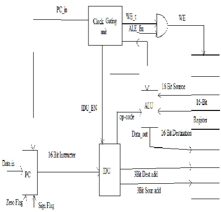
[image:1.595.315.538.397.611.2]Figure 1. Block diagram of a RISI Controller
The reduced instruction set interrupt controller (RISI Controller) architecture mainly consists of ALU (Arithmetic and logical Unit), Port Controller, Interrupt controller and Register Array and its block diagram is shown in the Fig. 1. It contains RISCPU, Interrupt controller, Port controller and Program flow controller. These blocks are connected by internal buses
2.1 Internal Architecture of RISC
Controller
execution of arithmetic and logical instructions and these are also useful for determine the flow of execution when branch and jump instructions take place. CPU checks the interrupt flag after completion of every instruction to know whether interrupt is available or not.ALU is capable of performing the Arithmetic (Like Addition and subtraction) and Logical operations (like And, Or, Xor and Cmpl). There are no special purpose registers in the CPU like accumulator and there is no priority among them. RISI Controller has multi read port and single write port. Generally read operations are performing during the positive edge of the clock and write operation is performing during negative edge of the clock. Stack is used to store up to four addresses during interrupt and Branch related instructions. Port controllers take care of the read and write operation. An 8-bit address value provided on the PORT bus together with a READ or WRITE strobe signal indicates the accessed port. The port address is either supplied in the program as an absolute value or specified indirectly as the contents of any of the eight registers. There are some specific instructions useful for the controlling of interrupt controller present in the RISI CONTROLLER
.
Fig. 2 Internal architecture of RISC processor
3. RISC CLOCK GATING ARCHITECTURE
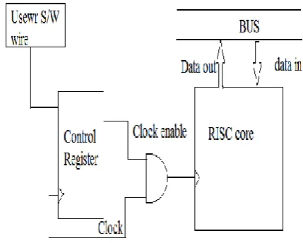
The power efficiency is the important constraint in designing portable computers, because lower power results in lower operating costs, lower fan noise, and lower cooling requirements. Therefore, designers of modern portable systems focus on increased system performance while reducing operating power consumption. Increasing the operating frequency, using more powerful, higher density chips achieves increased system performance, but increasing the performance level increases power consumption.
Power consumption can be controlled during system operation depending upon the processing workload. This approach is called dynamic voltage frequency scaling [4,13]. According to the CPU workload, there are synchronous between the variation of the operating frequency and supply voltage [14]. For the cases that the workload is less than the minimum supply voltage requirements to drive the CPU, the enable signal of the clock gating technique will activate, during the activation of the enable signal the CPU consumes zero power. Hence the minimum energy reduction will obtain The clock gating technique identifies low processing requirement periods and reduces operating voltage with clock
[image:2.595.324.541.161.290.2]frequency (voltage-frequency scaling), resulting in reduced average operating power consumption. According to the CPU workloads, f and V can be reduced to its minimum levels or zero levels based on the software control. Figure(4) shows the block diagram of the CPU dynamic energy reduction using clock gating technique
Figure”3.Block Diagram of Dynamic Power Reduction using Clock Gating technique.
The workload monitor, predict the RISC activities based on a software implementation, while the voltage frequency scaling unit implemented in hardware, with the clock gating design of figure 3 inside or before the RISC. The overall block diagram controls the RISC energy reduction by
- Controlling the supply voltage V.
- Controlling the operating Clock frequency f. - Turning the RISC power off during idle Periods.
The voltage-scaling unit accepts a command from the workload monitor, and generates the required supply voltage and clock frequency, or turns the RISC power off.
3.1 Clock Gating Technique for Low Power RISC processor
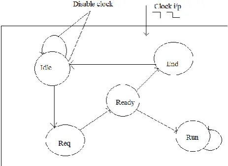
[image:2.595.58.273.305.477.2]“Figure”4.Principle of Low Power RISC Using FSM
When an IP core stays in the IS for some cycles, it does not need the clock. Therefore, ACG disables the IP clock if the following conditions are satisfied:
1. The current state of the IP core is IS. 2. There is no request for this IP on the system bus during the current cycle.
The conditions above also can be expressed as following: If the IP current state is IS and its next state is IS too, the clock is disabled automatically; otherwise, the clock is enabled. We call the circuit realizing the above logic Scout Circuit (SC) which is just a combinational one. The Clock Gating principle for low power IP design is shown in Fig.4
3. VLSI Implementation
In the previous chapter, the design considerations of different functional units are discussed. The VLSI implementation is described in this chapter.
3.1 VLSI Design Flow System Level Design Functional Design Functional Verification Logic Design
Logic Verification Circuit Design
Performance Evaluation Physical Design Layout Verification
System level design
It is used to create a high-level (Behavioural) representation
of the system. Tools used for system level design are Verilog,
VHDL and System C.
Functional design and verification
A functional design assures that each modular part of a device
has only one respons suability and performs that
responsibility with the minimum of side effects on other parts.
Functional verification in electronic design automation, is the
task of verifying that the logic design conforms to
specification.
Logic design
Translates system level description into transistors
o Many logic styles
o Schematic representation Logic verification
o Simplistic models - to verify functionality
o Fast - can run many cases
Circuit design
Calculates transistor sizes Performance evaluation
o Complex models - to evaluate timing and
power
o Slow - run only selected cases
Physical design
Translate schematic into layout
o Need to know the design rules
o Layout representation may not be similar
to schematic Logic verification
o Compare netlists
[image:3.595.61.293.76.244.2]o Simulators
4.2 VHDL Design Flow
Design Entry
The first step in the design process is to input your design into
a machine-readable format. To do this you will use a
Computer Aided Design (CAD) tool. A typical CAD tool
supports many design entry methods, such as a schematic
capture, HDL entry (VHDL/Verilog) or a component netlist.
In this course, all the designs are captured using VHDL.
Functional Simulation
Once a design has been captured, the next step is to simulate
it. This is done to ensure that the design will meet the
requirements of its specification. The first type of simulation
that is performed is a Functional Simulation. This is also
referred to as a Behavioural simulation in Xilinx Foundation.
Synthesis
During synthesis, the CAD tool will interpret your VHDL
design information and infer standard building blocks to
implement the. Subtle differences in your VHDL description
can result in different hardware being inferred at this stage.
Different hardware inferences will result in variances in
system performance.
Implementation
The Xilinx implementation process takes your design through
the TRANSLATE, MAP, and PLACE AND ROUTE
sub-processes. The TRANSLATE process convert the netlist
generated from the synthesis process, into a form specific to
the target device The PLACE & ROUTE process picks up
where the MAP process leaves off by allocating specific
resources (placing) and interconnecting (routing) the placed
design.
Device Configuration
After the design has been verified, a binary hardware
configuration file is generated (bitstream). This file is then
downloaded into the FPGA via the JTAG interface
.
Fig. 6 VHDL Design flow
5. CONCLUSION
The Interrupt control unit, Flow control unit of RISC Processor has been implemented successfully using XILINX in VHDL coding. Observed that about 20% of the power is saved by applying clock gating technique to the existing design. This design can be used for low power applications to enhance the battery life of the devices. Power can be reduced further by applying the clock gating technique at a higher level of granularity.
6. REFERENCES
[1] Deterministic Clock Gating for Microprocessor Power Reduction, Hai Li, Swarup Bhunia, Yiran Chen, T. N. Vijaykumar, and Kaushik Roy 1285 EE Building, ECE Department, Purdue University <hl, bhunias, yc, vijay, kaushik>@ecn.purdue.edu
[2] A Clock Gating Circuit for Globally Asynchronous Locally Synchronous Systems, Jonas Carlsson, Kent Palmkvist, and Lars Wanhammar Department of Electrical Engineering, Linkopings universitet SE-58 1 83 Linkoping Sweden
[3] AnEnergyEfic'ientHalf-tat"ic Cock-Gating D-Type Flip-Flop, Wing-Shan Tam, Oi-Ying Wong, Ka-Yan Mok, Chi-Wah Kok, Hei Wong
[4] A Novel Clock Distribution and Dynamic De-skewing Methodology, Ajun Kapoor* Nikhil Jayakumar' Sunil P Khatri'.* Department of EE, Texas A&M University, College Station TX 77843. * Department of ECE, University of Colorado, Boulder, CO 80309.
[5] Adaptive Clock Gating Technique for Low Power IP Core in SoC DesignXiaotao Chang 1,2, Mingming Zhang1,2, Ge Zhang1, Zhimin Zhang 1, Jun Wang1,21(Institute of Computing Technology, Chinese Academy of Sciences, Beijing, 100080, CHINA)
2(Graduate School of Chinese Academy of Sciences, Beijing, 100039, CHINA)
[6] CLOCK GATING ARCHITECTURES FOR FPGA
POWER REDUCTION, Safeen Huda, Muntasir Mallick, Jason H. Anderson, Dept. of ECE, Univ. of Toronto, Toronto, ON Canada, e-mail: {safeen.huda, muntasir.mallick, jason.anderson}@utoronto.ca
[7] Gated Clock Routing for Low-Power Microprocessor Design, Jaewon Oh and Massoud Pedram, Senior
Member, IEEE. IEEE TRANSACTIONS ON
COMPUTER-AIDED DESIGN OF INTEGRATED CIRCUITS AND SYSTEMS, VOL. 20, NO. 6, JUNE 2001
[8] LANG, T., MUSOLL, F , and CORTADELLA, J.: ‘Individual flip-flops with gated clocks for low power datapaths’, IEEE Trans. Circuits S y ~ tI.I , 1997, 44,( 6), pp. 507 516
[9] Low Power VLSI Design and Technology edited by G K Yeap (Motorola) & F N Najm (Univ. Illinois, Urban– Champaign)
[10]Logic Synthesis for Low Power VLSI Designs by Iman, Sasan, Pedram, Massoud