The Flexible DSP Accelerator Architecture
using Error Tolerant Adder
Ambily C Panicker1 , Sharon Mathew2
P.G. Student, Department of Electronics and Communication Engineering, Indira Gandhi institute of Engineering and
Technology for women, Nellikuzhy, Kerala, India1
Associate Professor, Department of Electronics and Communication Engineering, Indira Gandhi institute of
Engineering and Technology for women, Nellikuzhy, Kerala, India2
ABSTRACT:In the digital signal processing (DSP) domain, Hardware acceleration is proved an extremely promising implementation strategy. Instead of adopting a monolithic application-specific integrated circuit design approach, a novel accelerator architecture comprising flexible arithmetic components that support the execution of a large set of operation templates found in DSP kernels is introduced. One of its major peculiarity is to enable computations to be aggressively performed with carry-save (CS) formatted data. Incorporation of Error Tolerant Adder is another speciality. Advanced arithmetic design concepts, i.e., recoding techniques, and more enhanced arithmetic components are utilized enabling CS optimizations to be performed in a larger scope than in previous approaches.
KEYWORDS: Arithmetic optimizations, carry-save (CS) form, datapath synthesis, Error Tolerant Adder, flexible accelerator, operation chaining.
I.INTRODUCTION
Nowadays, intensive Digital Signal Processing (DSP) functions are required to be performed by the embedded systems. The incorporation of heterogeneity through specialized hardware accelerators improves performance and reduces energy consumption. Previously, application-specific integrated circuits, domain specific reconfigurable accelerators, Flexible DSP accelerators using carry-save arithmetic were used for this purpose.
The requirement of high performance with less power consumption and reduced area always leads to new researches and innovations. All these requirements are satisfied in this project. In the previous flexible DSP accelerator, fast operation chaining is achieved. But, it has high power consumption and area .So energy saving and small size are major consideration. Improved performance can also be achieved with this new accelerator
.
II.RELATEDWORK
In the early stages, application-specific integrated circuits (ASICs) form the ideal acceleration solution in terms of performance and power, but their inflexibility leads to increased silicon complexity, as multiple instantiated ASICs are needed to accelerate various kernels. Many researchers have proposed the use of domain-specific coarse-grained reconfigurable accelerators in order to increase ASICs’ flexibility without significantly compromising their performance.
High-performance flexible datapaths have been proposed to efficiently map primitive or chained operations found in the initial data-flow graph (DFG) of a kernel. The templates of complex chained operations are either extracted directly from the kernel’s DFG or specified in a predefined behavioral template library . Design decisions on the accelerator’s datapath highly impact its efficiency. Existing works on coarse-grained reconfigurable datapaths mainly exploit architecture-level optimizations, e.g., increased instruction-level parallelism (ILP). The domain-specific architecture generation algorithms vary the type and number of computation units achieving a customized design structure. Recently, aggressive operation chaining is adopted to enable the computation of entire subexpressions using multiple ALUs with heterogeneous arithmetic features.
The aforementioned reconfigurable architectures exclude arithmetic optimizations during the architectural synthesis and consider them only at the internal circuit structure of primitive components, e.g., adders, during the logic synthesis. However, research activities have shown that the arithmetic optimizations at higher abstraction levels than the structural circuit one significantly impact on the datapath performance. The timing-driven optimizations based on carry-save (CS) arithmetic were performed at the post-Register Transfer Level (RTL) design stage. The common subexpression elimination in CS computations is used to optimize linear DSP circuits. There developed some transformation techniques on the application’s DFG to maximize the use of CS arithmetic prior the actual datapath synthesis. The aforementioned CS optimization approaches target inflexible datapath, i.e., ASIC, implementations. Recently, a flexible architecture combining the ILP and pipelining techniques with the CS-aware operation chaining is introduced. However, all the aforementioned solutions feature an inherent limitation, i.e., CS optimization is bounded to merging only additions/subtractions. A CS to binary conversion is inserted before each operation that differs from addition/subtraction, e.g., multiplication, thus, allocating multiple CS to binary conversions that heavily degrades performance due to time-consuming carry propagations.
The existing accelerator architecture comprises flexible computational units (FCUs), which enable the execution of a large set of operation templates found in DSP kernels. It has a flexible datapath architecture that exploits CS optimized templates of chained operations. Each FCU can be configured to any of the different operation templates. The FCU enables intratemplate operation chaining by fusing the additions performed before/after the multiplication. It has good performance with large area and energy consumption.
III.ERRORTOLERANTADDER
A. Accurate Part
Accurate part starts from middle to MSB. Accurate part only Performs normal addition operations like ripple carry adder which is the most power-saving conventional adder but not like any fast adder.
B. Inaccurate Part
1. Check every bit position from left to right (MSB to LSB)
2. If both input bits are “0” or different, normal one-bit addition is performed
3. If both input bits are “1,” the checking process stopped and from this bit onward, all sum bits to the right are set to “1.”
In this method, high accuracy, great improvement in the speed performance and power consumption can be achieved. The inaccurate part consists of two blocks: control blocks and carry-free addition blocks. The carry free addition block is made up of modified XOR gates to generate a sum bit. The schematic implementation of the modified XOR gate is shown in Fig.1 which consist of M1, M2, M3 transistor and CTL is the control signal is coming from the control block.
Fig.1 Schematic implementation of carry-free addition block
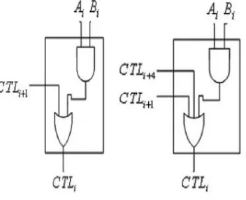
Control block is used to set the operational mode of the circuits. When CTL=0, the circuit to be operated in the normal XOR mode, while M1 and M2 are turned on and M3 are turned off. When CTL=1, it connecting the output node to VDD and hence setting the sum output to “1”, while M1 and M2 are turned off and M3 are turned on. The function of the control block is used to detect the first bit position when both input bits are “1” and set to the control signal on this position as well as those on its right to high. Consider design of 32-Bit error tolerant adder, it made up of 20 CSGCs and each cell generates a control signal at thecorresponding position in the carry free addition block.
Fig. 2 Control block of overall architecture
Fig.3 Schematic implementation of CSGS of Type 1& 2
The control signal generated by the leftmost cell of each group is connected to the input of the leftmost cell in the next group. Shaded portion in Fig. 2 represent the worst case propagation path. The extra connections allow the propagated high control signal to jump from one group to another instead of passing through all cells.
IV.CARRY-SAVE ARITHMETIC
Here, the aforementioned limitations are tackled by exploiting the CS to modified Booth (MB) recoding each time a multiplication needs to be performed within a CS-optimized datapath. Thus, the computations throughout the multiplications are processed using CS arithmetic and the operations in the targeted datapath are carried out without using any intermediate carry-propagate adder for CS to binary conversion, thus improving performance.
V.PROPOSEDFLEXIBLEACCELERATOR
The proposed flexible accelerator architecture is shown in Fig. 4. Each FAC operates directly on CS operands and produces data in the same form for direct reuse of intermediate results. Each FAC operates on 16-bit operands. Such a bit-length is adequate for the most DSP datapaths , but the architectural concept of the FAC can be straightforwardly adapted for smaller or larger bit-lengths. The number of FACs is determined at design time based on the ILP and area constraints imposed by the designer
.
Fig.4 Abstract of the flexible datapath
The CStoBin module is a ripple-carry adder and converts the CS form to the two’s complement one. The register bank consists of scratch registers and is used for storing intermediate results and sharing operands among the FACs. Different DSP kernels (i.e., different register allocation and data communication patterns per kernel) can be mapped onto the proposed architecture using post-RTL datapath interconnection sharing techniques . The control unit drives the overall architecture (i.e., communication between the data port and the register bank, configuration words of the FACs and selection signals for the multiplexers) in each clock cycle.
The structure of the FAC has been designed to enable high-performance flexible operation chaining based on a library of operation templates. Each FAC can be configured to any of the different operation templates. The proposed FAC enables intratemplate operation chaining by fusing the additions performed before/after the multiplication and performs any partial operation template of the following complex operations:
The following relation holds for all CS data: X̽ = {XC, XS} = XC + XS. The operand A is a two’s complement number. The alternative execution paths in each FCU are specified after properly setting the control signals of the multiplexers MUX1 and MUX2 . The multiplexer MUX0 outputs Y ̽ when CL0 = 0 (i.e., X̽+ Y is carried out) or ̽ Y ̽ when X̽−Y ̽ is required and CL0 = 1. The two’s complement 4:2 CS adder produces the N̽ = X̽ +Y ̽ when the input carry equals 0 or the N̽ = X̽−Y ̽ when the input carry equals 1. The MUX1 determines if N̽ (1) or K̽ (2) is multiplied with or divided by
A. The MUX2 specifies if K̽ (1) or N̽ (2) is added with the multiplication product. The multiplexer MUX3 accepts the output of MUX2 and its 1’s complement and outputs the former one when an addition with the multiplication product is required (i.e., CL3 = 0) or the later one when a subtraction is carried out (i.e., CL3 = 1). The 1-bit ace for the subtraction is added in the Error Tolerant Adder.These are the operations that can be carried out by the proposed FAC
.
Fig.5 FAC
The multiplier comprises a CS-to-MB module, which adopts a recently proposed technique to recode the 17-bit P̽ in its respective MB digits with minimal carry propagation. The multiplier’s product consists of 17 bits. The multiplier includes a compensation method for reducing the error imposed at the product’s accuracy by the truncation technique. However, since all the FAC inputs consist of 16 bits and provided that there are no overflows, the 16 most significant bits of the 17-bit W̽ (i.e., the output of the ETA, and thus, of the FAC) are inserted in the appropriate FAC when requested.
VII.EXPERIMENTALRESULT
Fig.4.1 Simulation result of the designed Flexible DSP accelerator
The accelerator proposed in this project is an optimum solution when considering power, delay and area. It can change the digital systems to a more comfortable zone, with small size, reduced energy consumption and faster operations. Incorporating a divider in the FAC makes the accelerator a better one. It will improve the performance, but may lead to large area. Anyway, it improves the performance of digital systems. Replacing components in the FAC may help it to handle more no.of bits which also improves the system performance.
VIII.CONCLUSION
A flexible accelerator architecture that exploits the incorporation of CS arithmetic optimizations to enable fast
chaining of additive, multiplicative and division operations is introduced. It improves the performance of DSP systems. The proposed flexible accelerator architecture is able to operate on both conventional two’s complement and CS-formatted data operands, thus enabling high degrees of computational density to be achieved .The Error Tolerant Adder improves the performance. Theoretical and experimental analyses have shown that the proposed solution forms an efficient design tradeoff point delivering optimized latency /area and energy implementations.
REFERENCES
[1] P. Ienne and R. Leupers, Customizable Embedded Processors: Design Technologies and Applications. San Francisco, CA, USA:Morgan Kaufmann, 2007.
[2] S. Xydis, G. Economakos, and K. Pekmestzi, “Designing coarse-grain reconfigurable architectures by inlining flexibility into custom arithmetic data-paths,” Integr., VLSI J., vol. 42, no. 4, pp. 486–503, Sep. 2009.
[4] Kostas Tsoumanis, Sotirios Xydis, Georgios Zervakis, and Kiamal Pekmestzi,” Flexible DSP Accelerator Architecture Exploiting Carry-Save Arithmetic” IEEE Trans.on Very Large Scale Integr. (VLSI) Syst.,2016
[5] Yuan Ho Chen, “An Accuracy –adjustment Fixed Width booth Multiplier based on Multilevel Conditional Probability”, IEEE Transaction on VLSI Systems,vol.23,Jan.2015
[6] P.Gouri, N. Ganeshkumar, K.Mohan Kumar “ Fixed width Booth multiplier for High- Speed Multilevel conditional probability Estimator”, Nov.5 2015,Vol.7