International Journal of Research in Advent Technology, Vol.7, No.6, June 2019
E-ISSN: 2321-9637
Available online at www.ijrat.org
doi: 10.32622/ijrat.762019104 140
Analysis of Modified Five Level Flying Capacitor Based
Multilevel Inverter
P.Siva Prasad, Dr.G.Annapurna
Abstract- Multilevel inverter concept gained importance because of high power handling capability and lower harmonic content in the output voltage. As the output voltage of multilevel inverters is synthesized from several levels of dc voltages, the harmonic distortion is minimum. Now -a- days, Carrier Based Pulse Width Modulation (CBPWM) technique gained importance as it can be easily extended to higher inverter levels and applied to Sinusoidal and Space Vector modulation schemes for control of multilevel inverters. This paper presents modified topology of Five level Flying Capacitor Multilevel Inverter with reduced number of dc bus capacitors and clamping capacitors. The performance of modified topology and normal topology Five Level FCMLI adopting Carrier Based Sinusoidal Pulse Width Modulation technique is evaluated in terms of THD in the output voltage. Simulation results based on MATLAB/SIMULINK are presented to verify effective compensation of harmonics when modified topology inverter is adopted.
Index Terms – Flying capacitor, multilevel inverter, CBPWM.
I. INTRODUCTION
Multilevel inverters are widely being used in high and medium power applications due low THD and high power handling capability. Now a days, there is a lot of literature about the topology and modulation schemes of multilevel inverter. The three topologies of multilevel inverters are Cascaded Multilevel Inverter (CMLI), Diode Clamp Multilevel Inverter (DCMLI), and Flying Capacitor Multilevel Inverter (FCMLI). [4]
Manuscript revised June 10, 2019 and published on July 10, 2019
P.Siva Prasad, Pursuing Ph.D from JNTUH Hyderabad
Dr.G.Annapurna, Department of Electrical & Electronics Engineering, G.Narayanamma Institute of Technology and Science (for Women), Hyderabad.
In Flying capacitor multilevel inverter, an extra capacitor is clamped to the power switches phase rail to supply the dc voltage level. These clamping capacitors help in reducing the switching states thereby allowing this structure of inverter to supply high voltages during the power outages.
A. Five Level Flying Capacitor basic topology Multilevel Inverter
This basic topology inverter uses clamping capacitors. The capacitor clamped switching cells are connected in series. These capacitors help in transferring limited amount of voltage to electrical devices. The switching stated in this type of inverter are same as that of diode clamped inverter. However, this inverter does not require clamping diodes. The drawback of the flying capacitor inverter is that the output is only half of the input DC voltage. In order to balance the flying capacitors, it suffers from switching redundancy within phase [1,2].
This flying capacitor topology consists of capacitors, diodes and switching devices. Even though the design of this topology can give infinite levels, it‟s usage it limited to six levels of voltage only due to practical limitations. In each leg there will switches and clamping capacitors. The capacitors near the source have high voltage while those connected adjacent to load carries lower voltage. The output voltage levels depend on the number of switches conducting in each leg. [5]
International Journal of Research in Advent Technology, Vol.7, No.6, June 2019
E-ISSN: 2321-9637
Available online at www.ijrat.org
doi: 10.32622/ijrat.762019104 141
distortion in the output voltage can be reduced by increasing the number of levels in the inverter output thus resulting staircase waveform. It is possible to optimize the switching sequence and size of capacitors to reduce the harmonic distortion in the output. [3]
The configuration of FCMLI is similar to that of DCMLI except that capacitors divide the input DC voltage. The voltage across each capacitor and each switch is Vdc. The voltage of the switching devices is limited by these capacitors.
For a 5-level flying capacitor multilevel inverter, No. of levels n=5, Number of switches=8 and Number of capacitors= 10.
Fig.1 shows one leg of a five level flying capacitor multilevel inverter. The switching states of this inverter are same as diode clamped multilevel inverter. For each output voltage level 4 switches should be turned ON. The switching states of 5-level flying capacitor clamped multilevel inverter are shown in Table.2 .
The switching angles are calculated in the similar manner done for diode clamped multilevel inverters. This process is carried out such that the THD in the output voltage is less.
Table.1 The switching pattern for capacitor clamped multilevel inverter.
Vo S1 S2 S3 S4 S5 S6 S7 S8 Vdc/2 1 1 1 1 0 0 0 0
Vdc/4 1 1 1 0 1 0 0 0
0 1 1 0 0 1 1 0 0
-Vdc/4 1 0 0 0 1 1 1 0
-Vdc/2 0 0 0 0 1 1 1 1
Fig.1 One phase of a 5-level Flying capacitor multilevel inverter
B. Modified 5-level Flying capacitor multilevel inverter:
International Journal of Research in Advent Technology, Vol.7, No.6, June 2019
E-ISSN: 2321-9637
Available online at www.ijrat.org
doi: 10.32622/ijrat.762019104 142
The five level modified topology FCMLI is shown in Fig.2. Each leg (phase) consists of 8 switching devices, 3 flying capacitors and 2 dc link capacitors. This FCMLI has four switching pairs (S1 S8), (S2 S7), (S3 S6) and (S4 S5). If one switch of the pair is switched ON, the other switch of same pair must be OFF. The dc link and flying capacitors will clamp the switches. The four switches (S1-S4) must be connected in series between dc input and load and same case even for other four switches (S5-S8). The three flying capacitors C1, C2and C3 are charged to different voltage levels. In order to produce different load voltages, the switching states are changed such that the capacitors and dc voltage are connected in different ways. Table 2 shows different switch combinations to get the required output voltage levels for five-level FCMLI. The advantage of this topology is that it require a single dc source to power the inverter.
Table: 2 Switching States of a Five-Level FCMLI
Vo S1 S2 S3 S4 S5 S6 S7 S8
Vdc/2 1 1 1 1 0 0 0 0
Vdc/4 0 1 1 1 0 0 0 1
Vdc/4 1 0 1 1 0 0 1 0
Vdc/4 1 1 0 1 0 1 0 0
Vdc/4 1 1 1 0 1 0 0 0
0 1 0 0 1 0 1 1 0
0 0 1 0 1 0 1 0 1
0 1 0 1 0 1 0 1 0
0 0 0 1 1 0 0 1 1
0 0 1 1 0 1 0 0 1
0 1 1 0 0 1 1 0 0
-Vdc/4 0 0 0 1 0 1 1 1 -Vdc/4 0 0 1 0 1 0 1 1 -Vdc/4 0 1 0 0 1 1 0 1 -Vdc/4 1 0 0 0 1 1 1 0 -Vdc/2 0 0 0 0 1 1 1 1
II. MODULATION TECHNIQUES
To reduce the Total Harmonic Distortion, different PWM schemes are developed. Multi carrier modulation scheme can be applied to MLI with some modifications to conventional PWM strategies.[6,7] There are different Multi carrier based modulation
techniques VIZ i) Phase Shift PWM ii) Phase disposition PWM iii) Phase Opposition Disposition PWM iv) Alternate Phase Opposition Disposition PWM v) Alternate Phase Shift PWM vi) Variable Frequency PWM vii) Alternate Variable Frequency PWM viii) Carrier Over Lap PWM.
In multilevel Inverters, modulation index is specified by the following equation.
( )
This paperr presents comparison between PD and POD SPWM schemes to trigger the devices of 5-level normal topology and modified topology capacitor clamped inverter.
A. PD-SPWM Control Techniques
In this scheme, in order to generate pulses, a triangular wave is compared with sinusoidal wave. This technique can be applied to multi-level inverter using several carrier waves. To generate „m‟ level output (m-1) carrier are required. In phase disposition technique, all the carriers above and below reference line have same magnitude, frequency and all are in same phase. This method is widely used as it results low harmonic distortion in output voltage.
Fig.3 PD- SPWM Technique
B. POD-SPWM Control Techniques
International Journal of Research in Advent Technology, Vol.7, No.6, June 2019
E-ISSN: 2321-9637
Available online at www.ijrat.org
[image:4.612.76.523.70.618.2]doi: 10.32622/ijrat.762019104 143
Fig.4 POD- SPWM Technique
[image:4.612.319.529.86.203.2]III. SIMULATION RESULTS
Fig. 5. Simulink diagram of 5-Level basic topology FCMLI
Fig.6 Simulink diagram of 5-Level modified topology FCMLI
Fig.7 Pulse Generation for Inverter
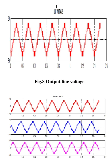
[image:4.612.77.290.193.410.2]A. Analysis of Five level normal topology inverter with PD CBPWM:
Fig.8 Output line voltage
[image:4.612.300.530.272.615.2]International Journal of Research in Advent Technology, Vol.7, No.6, June 2019
E-ISSN: 2321-9637
Available online at www.ijrat.org
doi: 10.32622/ijrat.762019104 144
Fig.10 FFT analysis of output line voltage
Fig.10 shows FFT analysis on inverter output line voltage and is found to be 20.08%.
Fig.11 Output phase voltage for one phase
Fig.12 Output phase voltages
Fig.13 FFT analysis of phase voltage
FFT is carried out on phase voltage of 5 level normal topology inverter and is 31.64%
B. Analysis of Five level normal topology inverter with POD CBPWM:
International Journal of Research in Advent Technology, Vol.7, No.6, June 2019
E-ISSN: 2321-9637
Available online at www.ijrat.org
doi: 10.32622/ijrat.762019104 145
Fig.15 Output line voltage
Fig.16FFT analysis of line voltage
Fig.16 shows FFT of line voltage of the five level inverter with POD CBPWM. The THD in the line voltage is found to be 25.48%.
Fig.17 Output phase voltages
Fig.18 Output phase voltage for one phase
Fig.19 FFT analysis of phase voltage
FFT is carried out on the phase voltage and the THD is found to be 31.66%.
C. Analysis of Five level new topology inverter with PD CBPWM:
International Journal of Research in Advent Technology, Vol.7, No.6, June 2019
E-ISSN: 2321-9637
Available online at www.ijrat.org
doi: 10.32622/ijrat.762019104 146
Fig.21 FFT analysis of line voltage
Fig.21 shows FFT analysis on line voltage of 5 level modified topology inverter and is found to be 17.76%.
Fig.22 Phase voltages of output voltage
Fig.23 FFT analysis of phase voltage
The FFT analysis carried out on phase voltage is shown in Fig.23 and the THD is found to be 28.07%.
D. Analysis of Five level modified topology inverter with POD CBPWM:
Fig.24 Output line voltage
Fig.25 Inverter output line voltages
International Journal of Research in Advent Technology, Vol.7, No.6, June 2019
E-ISSN: 2321-9637
Available online at www.ijrat.org
doi: 10.32622/ijrat.762019104 147
Fig.27 Output phase voltage for one phase
Fig.28 Output phase voltages
Fig.29 FFT analysis of phase voltage
Fig.26 and Fig.29 shows FFT analysis on 5 level modified topology inverter with POD CBPWM for line and phase voltages. The THD measured is found be 22.65% and 27.86% in line and phase voltages respectively.
Table.3: Results of Five Level normal and modified topology FCMLIwith PD and POD CBSPWM Control Schemes. S. No. Control Scheme % THD NORMAL TOPOLOGY MODOFIED TOPOLOGY PHASE VOL-TAGE LINE VOL-TAGE PHASE VOL-TAGE LINE VOL-TAGE
1. PD CB SPWM
31.64 20.08 28.07 17.76
2.
POD CB
SPWM 31.66 25.48 27.86 22.65
From the aboveTable.3, it is clear that % THD in the output voltage is low for modified topology five level inverter compared to normal topology inverter. It is also proved that the harmonic content in the output is less with PD CBPWM control method than that of POD CBPWM method.
IV. CONCLUSION
The Five level Flying Capacitor of normal topology and modified topology are simulated employing CBSPWM control scheme. In order to validate the performance of both topologies of 5 Level inverter, simulation is carried out with PD CBPWM and POD CBPWM technology. The simulation results prove that the % THD in the output voltage of modified topology is less compared to normal topology. It is also observed that the % THD is less with PD CBPWM when compared to POD CBPWM method. It is concluded that the performance of 5 level modified topology inverter is superior when compared to that with normal topology.
REFERNCES
[1] Ada Olokpo, Goshwe Nentawe, David O. Agbo,“Three-Phase Five-Level Flying Capacitor Multilevel inverter For Harvesting Solar Power”,International Journal of Engineering Science Invention (IJESI), Vol.7 Issue.4, PP 30-39, April 2018. [2] Sayli Khadse,Rohini Mendole, Amarjeet Pandey, “A 5-Level
Single Phase Flying Capacitor Multilevel Inverter”, International Research Journal of Engineering and Technology (IRJET), Vol.4 Issue.2,pp348-352,Febrauary,2017.
[3] J.Rodriguez, J.S.Lai and F.Z.Peng, ”Multilevel inverters survey of
topologies control and Applications“,IEEE
Trans.Ind.Electron,vol 49,pp 724-738,2002.
International Journal of Research in Advent Technology, Vol.7, No.6, June 2019
E-ISSN: 2321-9637
Available online at www.ijrat.org
doi: 10.32622/ijrat.762019104 148
System”, International Journal of Current Engineering And Technology, Special Issue-3, 2014.
[5] L.Xu, and V.G.Agelidisd, “Active capacitor voltage control of flying capacitor multilevel converters”, IEEE Proc. Electr. Power Appl., vol. 151, no.3, pp. 313-320, May. 2004.
[6] C.Feng, J.Ling, and V.G.Angelidis, “Modified phaseshifted PWM control for flying capacitor multilevel converters”, IEEE Trans. Power Electron., vol. 22, no.1, pp. 0178-0185, Jan. 2007. [7] Sourabh Rathore, Mukesh Kumar Kirar and S.K Bhardwaj,”
Simulation of Cascaded H-Bridge Multilevel Inverter using PD, POD, APOD Techniques”, Electrical & Computer Engineering: An International Journal (ECIJ) Volume 4, Number 3, September 2015.
AUTHORS PROFILE
P.Siva Prasad Completed B.Tech Electrical & Electronics Engineering in 2008 from AITS, Rajampet affiliated to JNTUH, M.Tech in Electrical Engineering in 2010 from NIT Calicut, kerala and Pursuing Ph.D from JNTUH Hyderabad. Currently Working as Assistant Professor at G.Narayanamma Engineering college (for women) affiliated to JNTU, Hyderabad with 8 Years of experience. His areas of interest include Power Electronics.