Tri-Mode Bandwidth-Tunable Filter Based on Microstrip-to-CPW
Resonator
Jian-Quan Huang1, * and Zhi-Han Chen2
Abstract—A novel microstrip-to-CPW resonator is presented, which can be employed to design bandwidth-tunable bandpass filter. The tri-mode resonator is composed of a dual-mode microstrip resonator and a CPW stub printed on a single piece of substrate. Two varactors embedded in the resonator are utilized to adjust the frequencies of the first and third resonant modes independently, thus flexible bandwidth control can be achieved. For demonstration, a prototypical filter is implemented with fixed center frequency of 1.72 GHz and 9.3%–32.6% fractional bandwidth (FBW) tuning range. Good agreement is obtained between the simulated and experimental results.
1. INTRODUCTION
With the rapid development of wireless communication technology, the demand for reconfigurable filters is increasing due to their potential to reduce the circuit size and cost. Microwave reconfigurable filters have been studied for decades, and most of the reported filters focus on the tunability of center frequency [1–3]. In some cases, filters with tunable bandwidth are more desirable than filters with tunable center frequency. However, compared with frequency agility, bandwidth control is much more difficult to be achieved because of the complexity to adjust the inner coupling level.
As research continues, several design methods of bandwidth control have been published [4–6]. In order to obtain controllable inner coupling, a short transmission line and a pair of varactors between resonators were utilized to create controlled magnetic and electric couplings, respectively [4]. In [5], a T-type varactor network between resonators was devised to adjust the coupling coefficient, thus a tunable bandwidth was acquired. Both [4] and [5] use extra controlled coupling network to achieve bandwidth control, which significantly increases the complexity and loss of the filters with more tuning elements. A dual-band bandpass filter was proposed in [6], whose bandwidths can be adjusted by controlling odd-and even-mode resonant frequencies of dual-mode resonators. Nevertheless, most of the tunable filters, such as those mentioned above, only work for narrow-band applications. Studies on wideband tunable filters with controlled bandwidth have less been reported [7].
This paper presents a wideband reconfigurable bandpass filter with tunable bandwidth based on a tri-mode microstrip-to-CPW resonator [8]. The resonator consists of a dual-mode resonator on the top layer and a CPW stub occupying the bottom layer. Specially, the first and third resonant modes of this resonator can be tuned individually, which supplies sufficient degree of freedom to adjust both edges of the passband of a tunable bandpass filter. Varactors are utilized to add tuning ability to the bandwidth of the filter. Without increasing circuit size and extra controlled coupling network, low-loss wideband tunable filters with flexible bandwidth control can be implemented with much simpler structures and less tuning components. Finally, the proposed tunable filter is fabricated and measured. Measurement and simulation agree well, which verifies the correctness of the theoretical analysis.
Received 23 May 2017, Accepted 14 July 2017, Scheduled 26 July 2017
* Corresponding author: Jian-Quan Huang ([email protected]).
1 School of Electronic Information and Electrical Engineering, Xiangnan University, Chenzhou, Hunan, China.2School of Electronic
(a) (b)
Figure 1. Layouts of the proposed reconfigurable filter. (a) Top view and (b) Bottom view.
2. DESIGN OF THE RECONFIGURABLE BANDPASS FILTER WITH TUNABLE BANDWIDTH
Figure 1 depicts the layouts of the proposed reconfigurable bandpass filter. As shown in Figure 1(a), the top layer consists of a modified T-shaped dual-mode resonator and I/O ports. For significantly reducing the size of the filter, the dual-mode resonator is bent, and a T-shaped stub is adopted. The center-tapped stub can not only contribute an additional transmission pole, but also create an extra TZ located at lower stopband. On the bottom layer as depicted in Figure 1(b), a microstrip dual-mode resonator and a CPW stub are connected by a metal via hole to build a tri-mode resonator. Two varactors (C1
and C2) reversely biased by DC powers V1 and V2 are embedded in the CPW and microstrip stubs,
respectively. Also, an extra via hole is inevitably introduced to ensure thatC2 works properly. The via
hole and resonator are connected by a high-Q chip inductor, which will eliminate the effects of the via hole from the resonator.
2.1. Resonance Properties of the Tri-Mode Resonator
Figure 2(a) illustrates the structure of the microstrip-to-CPW resonator, which is equivalent to the microstrip crossed resonator shown in Figure 2(b). Two varactors embedded at both layers of the structure. C1 connects the CPW stub and the ground, while C2 is embedded in the microstrip open
stub. The proposed resonator is symmetrical, thus even- and odd-mode analysis can be applied to explain the tri-mode resonant characteristics. Then, the odd- and even-mode equivalent circuits are depicted in Figure 3. As shown in the figure,Y1,Y2,Y3,θ1,θ2 andθ3 refer to characteristic admittances
and electrical lengths for the transmission line sections, respectively. The odd- and even-mode input admittances of the resonator are given by
Yin odd = −jY1cotθ1 (1)
Yin even1 = jY1tanθ1−
j 2
ωY3C1+Y32tanθ3
Y3−ωC1tanθ3
(2)
Yin even2 = jY1tanθ1+
YmYv
Ym+Yv (3)
Ym = j 2
Y2Y3tanθ2+Y22tanθ2
Y2−Y3tan2θ2
(4)
Yv = jωC2Cb C2+Cb
(5)
whereCb is the dc block with 51 pF. According to the resonant conditions expressed as follows,
Yin odd = 0 (6)
all three resonant frequencies can be calculated. It is obvious that both even-mode frequencies can be adjusted by C1 and C2, whereas the odd-mode frequency is fixed. This theoretical conclusion can be
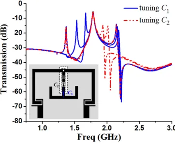
verified by EM simulation in the case of weak I/O coupling as shown in Figure 4. Figure 4 illustrates that the bandwidth can be changed byC1 andC2, while the center frequency is fixed. By adjusting the
capacitance of the varactors, both sidebands can be adjusted independently of each other, which add great flexibility to the bandwidth control.
(a) (b)
Figure 2. (a) Microstrip-to-CPW resonator. (b) Equivalent microstrip crossed resonator.
(b)
(a) (c)
Figure 3. Equivalent circuits of the resonator. (a) Odd-mode circuit. (b) The first even-mode circuit. (c) The second even-mode circuit.
Figure 4. EM Simulations under weak I/O coupling with differentC1 and C2.
2.2. Design Procedures of the Reconfigurable Filter
On the foundation of the above theoretical analysis, detailed design procedures of the proposed bandpass filter with tunable bandwidth are described as follows:
Step 1) Decide the center frequency of the reconfigurable filter:
In order to simplify designing, odd-mode resonating frequency fodd is selected as the center frequency. Obviously,θ1 is initially set as λ/4 atfodd.
Step 2) Design of the tuning ranges of two even-mode resonating frequencies:
Based on the equivalent circuit analysis, θ1+θ3 can be roughly selected as λ/4 at the first
even-mode resonating frequencyfeven1, whileθ1+ 2θ2 should be chosen aroundλ/2 at the second even-mode
resonating frequencyfeven2.
Then, the tuning ranges of two even-mode resonating frequencies can be calculated by using Eqs. (2)–(7). There are five or more degrees of freedom (i.e., Y1, Y3, θ1, θ3, C1 for feven1, and Y1,
Y2,Y3,θ1,θ2,C2forfeven2) to determine the tuning ranges. The admittances and electrical lengths are
chosen first, then the changes of even-mode resonating frequencies versus capacitances can be obtained. Step 3) Trim and optimize the parameters:
The final optimization is performed using EM/circuit cosimulation in Agilent’s Advanced Design System (ADS). Some unexpected effects including via-hole effects, losses of lumped elements and radiation of the slots are taken into account when all parameters are finalized.
3. FILTER IMPLEMENTATION AND RESULTS
In order to prove the validity, the filter is fabricated on a substrate with relative permittivity of 2.55 and thickness of 0.8 mm as shown in Figure 5. All dimensions are determined as follows: L1 = 29.0,
L2 = 10.8, L3 = 10.8, L4 = 29.8, L5 = 17.1, L6 = 7.4, W1 = 2.2, W2 = 0.8, W3 = 0.4, W4 = 2.0,
g1= 0.3,g2 = 0.4,R= 0.4 (all in mm). Varactors used in this work are SMV-1413 from SKYWORKS,
while the chokes are 100nH high-Q chip inductors of MURATA. The overall size of the fabricated filter is 0.19λ0×0.14λ0.
(a) (b)
Figure 5. Photos of the fabricated reconfigurable filter. (a) Top view. (b) Bottom view.
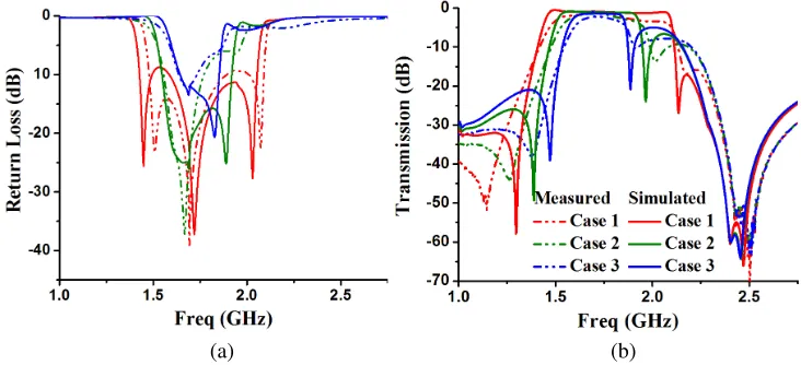
Figure 6 depicts the comparisons of simulated and measured S-parameters of the prototypical filter. All S-parameters are measured by the Agilent 5230A network analyzer. Figure 6(a) illustrates that lower sideband of the reconfigurable filter has a tuning range of 140 MHz (1.50–1.64 GHz), whenV1
varies from 0.2 to 1.6 V. The upper sideband of the filter, as shown in Figure 6(b), has a tuning range of 260 MHz (1.80–2.06 GHz) whenV2 varies from 0 to 7.1 V. Therefore, the reconfigurable filter reports a
(a) (b)
Figure 6. Measured and simulatedS-parameters of three cases. Case 1: V1 = 0.2, V2 = 7.1; Case 2:
V1= 0.8,V2 = 1.8; Case 3: V1 = 1.6,V2 = 0.
Table 1. Comparisons with other reported tunable filters.
Ref.
Center Frequency
(GHz)
FBW Tuning range (%)
Insertion Loss (dB)
Number of TZs
Number of Tuning Elements*
Size (λg)
[4] 1.85 2.2–9.2 3.1–6.5 2 6 0.24×0.25
[5] 1.70 2.9–6.5
(1-dB BW) 3.8–4.9 2 5 0.12×0.07
[6] 1.74
(1st passband) 5.8-8.6 2.0–4.4 1 1 0.21×0.21
[7] 2.0 22–34 0.8 2 6 NG
Proposed
Filter 1.72 9.3–32.6 1.1–2.2 3 2 0.19×0.14 * Only the tuning elements contributed to tunable bandwidth of the reported tunable filters are considered.
NG: not given
Agreement between the simulated and measured results is reasonable. Some errors may be attributed to the fabrication and loss of the lumped components. Finally, Table 1 compares the prototypical filter with several reported bandwidth-tunable filters. The proposed reconfigurable filter has a good bandwidth-tunable performance with a clear and simple design.
4. CONCLUSIONS
In this paper, a concise method of designing bandwidth-tunable filter based on multi-mode resonator is proposed. A double-layer microstrip-to-CPW resonator is analyzed in theory to validate this design method. By tuning the first and third resonating modes of the resonator independently, a reconfigurable bandpass filter with tunable bandwidth is successfully designed, fabricated and tested. Due to the novel microstrip-to-CPW resonator, circuit size of the proposed filter is notably reduced. Measured and simulated results are in good agreement to prove the design concepts.
ACKNOWLEDGMENT
REFERENCES
1. Hsieh, L.-H. and K. Chang, “Tunable microstrip bandpass filters with two transmission zeros,”
IEEE Transactions on Microwave Theory and Techniques, Vol. 51, No. 2, 520–525. Feb. 2003. 2. Ahn, C. H., D. J. Jung, and K. Chang, “Compact parallel-coupled line bandpass filter using double
complementary split ring resonators,” Microwave and Optical Technology Letters, Vol. 55, No. 3, 506–509, Mar. 2013.
3. Chen, Z. H. and Q. X. Chu, “Reconfigurable bandpass filter with electric coupling and constant absolute bandwidth,” Microwave and Optical Technology Letters, Vol. 58, No. 6, 1401–1404, Jun. 2016.
4. Chiou, Y. C. and G. M. Rebeiz, “A tunable three-pole 1.5–2.2-GHz bandpass filter with bandwidth and transmission zero control,”IEEE Transactions on Microwave Theory and Techniques, Vol. 59, No. 11, 2872–2878. Sep. 2011.
5. Chi, P. L., T. Yang, and T. Y. Tsai, “A fully tunable two-pole bandpass filter,” IEEE Microwave and Wireless Components Letters, Vol. 25, No. 5, 292–294, Mar. 2015.
6. Chaudhary, G., Y. Jeong, and J. Lim, “Dual-band bandpass filter with independently tunable center frequencies and bandwidths,” IEEE Transactions on Microwave Theory and Techniques, Vol. 61, No. 1, 107–116. Nov. 2013.
7. Huang, X., Q. Feng, and Q. Xiang, “Bandpass filter with tunable bandwidth using quadruple-mode stub-loaded resonator,” IEEE Microwave and Wireless Components Letters, Vol. 22, No. 4, 176–178, Apr. 2012.