Design of Power Droop Reduction Scan Based Rc Logic Bist
Vemula Nagarjuna & K.Babu Rao
1M.tech-Scholar, Dept of ECE, universal college of engineering and technology, Guntur, India 2Assistant Professor, Dept of ECE, universal college of engineering and technology, Guntur, India
ABSTRACT: Built-in self-test (BIST) is an attractive approach to detect delay faults because of its inherent support for at-speed test. RC logic BIST (RCLBIST) is a technique that has been successfully applied to stuck-at fault testing. As delay faults have lower random pattern testability than stuck-at faults, the need for RCLBIST schemes has increased. However, an extension to delay fault testing is not trivial as this necessitates the application of pattern pairs. As a consequence, delay fault testing is expected to require a larger mapping effort and logic overhead than stuck-at fault testing. With this in mind, we consider the RC fault model, which is widely used for complexity reasons, and an extension of a RCLBIST scheme for transition fault testing is presented. Rows and column logic BIST is applied to the memory array to make the error free operation. As in single vector address memories faces many problems like stuck at faults, to overcome this we are applying two vector addresses for memories. The two vectors are called as row and column. The total simulation is done in xilinx 14.7.
Index Terms: Power Droop (PD), Stuck-at Faults, Built-in self-test (BIST), Row Column Logic BIST (RCLBIST)
I. INTRODUCTION
It becomes most significance for testing various kinds of defects rapidly and precisely for reducing the cost of testing and to improve the quality of memory, mostly in a system-on-a-chip design environment. Memory defects can be modelled as coupling, stuck-at, transition, pattern-sensitive faults, and address decoder, and it is considered that the failures are because of leakage defects.
Among the different testing algorithms BIST (built-in self test) techniques have
been hugely adopted for the embedded memories.
Memory test patterns can be produced deterministically or randomly through either equipment of test or BIST circuitry. Test patterns are randomly produced which can identify not only modelled defects but also timing and non-modelled defects. Nevertheless, deterministic Row Column BIST (RC BIST) patterns, for their simplicity, are widely adopted for BIST and chip testing. Some hardwired memory BIST techniques have been improved, and recently some circuits of
micro-coded memory BIST were
implemented for embedded Memories.
In general micro-coded memory BIST techniques have great exibility in applying various test patterns combinations for static and dynamic defects. Memory retention faults and conventional static faults are the major targets, with a register or SRAM storing micro-codes. We introduce a various micro-coded BIST technique which aims for capturing the address decoder open faults additional to the conventional static faults. Furthermore, a certain degree of neighbourhood pattern-sensitive faults are identified by
cellular-automata-based address and pattern
generators.
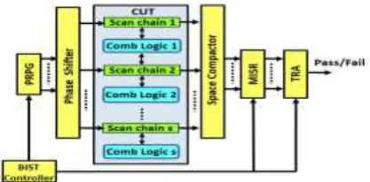
In our scalable approach, one (or more) test vector to be applied to the CUT according to conventional scan-based LBIST is replaced by new, proper test vector, referred to as substitute test vector. The Substitute Test (ST) vector(s) is obtained based on the test vectors to be applied at previous and future capture phases in order to reduce the maximum number of transitions between any two following test vectors. This way, the Circuit under Test (CUT) and Power Droop (PD) are reduced compared with the original test sequence. We examine the presence of a phase shifter (PS), which is commonly acquired in scan-based LBIST to reduce the correlation among the test vectors applied to adjacent scan-chains. In our approach, this property is exploited for enabling its hardware implementation of low-cost. Then our method can be acquired if the PS does not provide the previous and future test vectors for all scan-chains or if the scan-based LBIST does not present a PS.
Our scheme is scalable in the desirable PD reduction. Hence, test engineers could choose the proper activity factor (AF) in order to avoid the following:
Fig 1. Schematic of the considered Scan-based LBIST Architecture
1) Faulty chips being tested as good (due to an induced too low activity factor (AF),
lower than that experienced during normal operation).
2) Good chips being tested as faulty (due to an induced excessive activity factor (AF), higher than that experienced during normal operation).
PD scalability is acquired by scaling the number of ST vectors to be applied among original test vectors. Our existed approach can reduce the maximum AF among the following capture phases when compared with conventional scan-based LBIST. This is obtained without maximizing the number of test vectors over conventional scan-based LBIST for a given target fault coverage (FC). Furthermore, our method requires a very limited area overhead (AO) compared with conventional scan-based LBIST. In addition, our solution requires substantially less test vectors to achieve a target FC compared with the alternative solutions.
III. PROPOSED SYSTEM
Address Location: Address location is
the major topic these days. Hence,
everyone expects privacy in their
accounts, mails, sending of messages, and in all their communication modes. But, by using older methods, older versions of
technology those messages or
communications going in wrong way or wrong person.
Lets consider an example by taking a matrix that is with the binary numbers.
[
The message send to the address of 0101, but there is possibility of going the message to another address that is of 01 00. Hence, the target was missed by far. Thus, privacy was disturbed. Another person dragged message. If it is official notice or a secret code, then there will lot of damage to the nation.
In this existing system the following combinations will be available.
A1 - 000
A2 - 001
A3 - 010
A4 - 011
A5 - 100
A6 - 101
A7 - 110
A8 - 111
So the file or the message want to send will reach any of the above address. So it is very difficult to get the correct information and it is very problematic to the nations that the secrets or privacy will be loose. This is the reason to get the new version of the system to store and get the information.
Purpose of Storage: While using of former
storage system, the target of the storage will be altered due to wrong address locator. For example, if want to store the file in one place at RAM, i.e., at 01 01 in the above matrix, there is a chance to store in 01 11 or 01 00. To overcome this problem the following new system has been introduced. In this proposed system, we will use the column and row system.
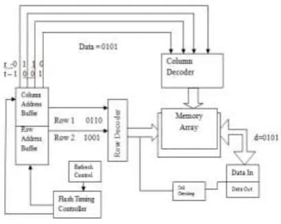
The new address matrix system will send the file or message we want to send will reach the exact position i.e., our target.
For example: [
1 0 1
1 1 0
1 0 0
]
In the proposed system there are two locators i.e., column address and row address buffer which are send the files to the column decoder and row decoder respectively. Further, they will be sent to the memory array which are indicated as columns and rows as 0110 & 1001 respectively. The data I want to send is 0101 and is located at memory array and the data will reach into the data in or data out as 0101. There is no change of address by using this system.
Figure 2: proposed system
Column Address : Buffer An address
generates the control signal at the first level while the semiconductor memory device performs data accessing operations, thereby reducing or minimizing the output of an internal address buffered and output by the address buffer at and thus reducing power consumption during no-operation states of the semiconductor memory device.
Row address buffer: Row address buffer
gets the data from the refresh control and the flash timing controller and sends to the row decoder to decode the data.
Column Decoder: A memory having
multiplexed address inputs uses a column decoder which is deactivated during row address time and becomes activated during column address time. Access time and power dissipation are reduced since the column decoder need not be fully recovered after row address information has terminated and column address information is available.
Traditionally, RAM, or Random Access Memory, was used to describe a memory which offered the same access latency for all its memory locations. This is barely the case with modern DRAM systems. Use an 8K x 32 SRAM = 256 Kb = 218
218= 29 rows x 29 columns. Row decoder is 9 to 512 decoder.
Every 32 (25) columns is a ‘word’, and we only need to decode words. So, column decoder needs to decode 24 words, so need a 4 to 16 column decoder.
Memory Array: The data came from
column decoder and row decoder will be
stored at the Memory Array and further it will be transferred to data out.
Typically want an aspect ratio that is not too far from square assertion of word line accesses all cells in a row Not all bits that are read from a row may be used. Loading on word line is high! Sense Amp function is to detect bit line change and produce a full ‘0’ or ‘1’ for output latch. The first array-based memory chips are expected to become available with a storage capacity of up to 100 gigabytes (GB) per chip. Potential applications are similar to those of current USB flash drives and solid-state hard drives.
Cell Checking: Westinghouse has
provided cell structure replacement parts as listed in DB Air Circuit Breaker and Cell Parts Listing. Westinghouse, with its extensive nuclear power experience and access to the original Westinghouse nuclear plant design documents, has built new DB circuit breakers for several power plant operations. Use of the new cell-checking device quickly provides evidence of whether the cell structure needs maintenance or possible parts replacement.
Flash Timing Controller: NOR Flash
memory provides random access
capabilities to read and write data in specific locations in the memory without having to access the memory in sequential mode. Its high-speed read capacity allows the NOR Flash memory to be the first choice for code storage and direct execution in a variety of systems from computer BIOS to portable electronic
devices. The command codes are
combined with addresses and data, and are written sequentially to the command
registers using microprocessor write
Refresh Control: A UI Refresh Control object provides a standard control that can be used to initiate the refreshing of a table view’s contents. You link a refresh control to a table through an associated table view controller object. The table view controller handles the work of adding the control to the table’s visual appearance and managing the display of that control in response to appropriate user gestures.
IV. RESULTS
Fig 3. RTL Schematic
Fig 4. Technology Schematic
Fig 5. Output
V.CONCLUSION
We have presented a novel approach to reduce peak power and power droop during the capture cycles in Row Column Logic BIST (RCLBIST), thus reducing the probability that the induced delay effect is erroneously recognized as presence of a delay fault, with consequent erroneous generation of a test fail. We showed that
our approach allows reducing by
approximately the power consumption using algorithm in the scan chains on design itself with respect to standard RC LBIST. We also showed that our approach reduces area and time delay inside the process .The proposed approach exhibits no impact on increasing power, delay and area respectively.
VI. REFERENCES
[1] J. Rajski, J. Tyszer, G. Mrugalski, and B. Nadeau-Dostie, “Test generator with preselected toggling for low power built-in self-test,” in Proc. Eur. Test Symp., May 2012, pp. 1–6.
[2] Y. Sato, S. Wang, T. Kato, K. Miyase, and S. Kajihara, “Low power BIST for scan-shift and capture power,” in Proc. IEEE 21st Asian Test Symp., Nov. 2012, pp. 173–178.
[3] E. K. Moghaddam, J. Rajski, M. Kassab, and S. M. Reddy, “At-speed scan test with low switching activity,” in Proc. IEEE VLSI Test Symp., Apr. 2010, pp. 177–182.
[5] I. Polian, A. Czutro, S. Kundu, and B. Becker, “Power droop testing,” IEEE Design Test Comput., vol. 24, no. 3, pp. 276–284, May/Jun. 2007.
[6] X. Wen et al., “On pinpoint capture power management in at-speed scan test generation,” in Proc. IEEE Int. Test Conf., Nov. 2012, pp. 1–10.
[7] S. Kiamehr, F. Firouzi, and M. B. Tahoori, “A layout-aware X-filling approach for dynamic power supply noise reduction in at-speed scan testing,” in Proc. IEEE Eur. Test Symp., May 2013, pp. 1–6.
[8] M. Nourani, M. Tehranipoor, and N. Ahmed, “Low-transition test pattern generation for BIST-based applications,” IEEE Trans. Comput., vol. 57, no. 3, pp. 303–315, Mar. 2008.
[9] N. Z. Basturkmen, S. M. Reddy, and I. Pomeranz, “A low power pseudorandom BIST technique,” in Proc. 8th IEEE Int. On-Line Test. Workshop, Jul. 2002, pp. 140–144.
[10] J. Rajski, N. Tamarapalli, and J. Tyszer, “Automated synthesis of large phase shifters for built-in self-test,” in Proc. Int. Test Conf., Oct. 1998, pp. 1047– 1056.
[11] P. Girard, L. Guiller, C. Landrault, S. Pravossoudovitch, and H. J. Wunderlich, “A modified clock scheme for a low power BIST test pattern generator,” in Proc. IEEE VLSI Test Symp., Apr./May 2001, pp. 306–311.
[12] G. Hetherington, T. Fryars, N. Tamarapalli, M. Kassab, A. Hassan, and J.
Rajski, “Logic BIST for large industrial designs: Real issues and case studies,” in Proc. Int. Test Conf., 1999, pp. 358–367.
[13] M. Tehranipoor, M. Nourani, and N. Ahmed, “Low transition LFSR for BIST-based applications,” in Proc. 14th Asian Test Symp., Dec. 2005, pp. 138–143.
[14] Y. Huang and X. Lin, “Programmable logic BIST for at-speed test,” in Proc. 16th Asian Test Symp., Oct. 2007, pp. 295– 300.
[15] X. Lin, E. Moghaddam, N.