University of Connecticut University of Connecticut
OpenCommons@UConn
OpenCommons@UConn
Doctoral Dissertations University of Connecticut Graduate School 12-17-2019Exploiting Memristors for Compressive Sensing Applications
Exploiting Memristors for Compressive Sensing Applications
Fengyu QianUniversity of Connecticut - Storrs, [email protected]
Follow this and additional works at: https://opencommons.uconn.edu/dissertations
Recommended Citation Recommended Citation
Qian, Fengyu, "Exploiting Memristors for Compressive Sensing Applications" (2019). Doctoral Dissertations. 2393.
Exploiting Memristors for Compressive
Sensing Applications
Fengyu Qian, Ph.D. University of Connecticut, 2020
ABSTRACT
The amount of sensory signal is increasing dramatically as we’re stepping into the era of Internet of Things (IoT). Compressive Sensing (CS), feature as Sub-Nyquist sampling rate and low complexity sensing architectures, is very promising for these kinds of applications where resources are restricted. Through applying this novel compression technology, data size of sensory signals are largely compressed such that it is very efficient within the signal processing, data transmitting and storage pro-cesses. Compared to conventional codec method, CS technique requires less hardware resources and achieve lower power consumption within sensor nodes.
However, there are several bottle-necks of existing compressive sensing imple-mentation, which discourage the utilization in practical applications. Based on our continues studies, memristor devices are exploited to design the compressive sensing system for sensory signals with multiple functions.
First of all, memristor is utilized as random number generator for sensing matrix, and in-memory computing is also achieved based on array structure. A new memristor model is proposed to evaluate its feasibility of being utilized with CS applications
Fengyu Qian, University of Connecticut, 2020
application of video streaming. Inside the proposed system, memristor devices are also used to implement the control logic for real time compression rate optimizations. Afterwards, a new prior algorithm is proposed by us to further improve the CS process with higher compression ability. The utilization of memristor is extended to the generation of prior information. Evaluation results demonstrate the advantages of our work in different aspects. In general, our proposed CS system can achieve higher energy efficiency, less hardware complexities, and with very good recovery quality, compared to existing implementations of both CS system and conventional codec method.
Exploiting Memristors for Compressive
Sensing Applications
Fengyu Qian
B.S., Xi’an Jiaotong University, 2012
A Dissertation
Submitted in Partial Fulfillment of the Requirements for the Degree of
Doctor of Philosophy at the
University of Connecticut
Copyright by
Fengyu Qian
APPROVAL PAGE
Doctor of Philosophy Dissertation
Exploiting Memristors for Compressive
Sensing Applications
Presented by Fengyu Qian, B.S., Major Advisor Lei Wang Associate Advisor Mehdi Anwar Associate Advisor Faquir Jain University of Connecticut 2020ACKNOWLEDGMENTS
First of all, I would like to give my deepest grateful appreciation to my advisor, Dr. Lei Wang for his help and support all over my graduate studies in UConn. He uses his immense knowledge to help me with finding the research direction, developing theories and algorithms, establishing experiments, and solving practical problems along my Ph.D. works and beyond. This thesis wouldn’t be completed without his help and guidance. I’d like to also thank him for leading me to step into the career of IC designs. Besides, he is very gentle and always consider for others, and it’s really great to work with him.
Secondly, I would like to express my great appreciation to the rest of my committee members: Dr. Mehdi Anwar, Dr. Faquir Jain, and committee witness members: Dr. Rajeev Bansal and Dr. Helena Silva. Your insightful comments, feedback and suggestions were invaluable to the completion of this thesis. And also, I want to thank you for making every communication to be a very pleasant learning process. It’s my greatest pleasure to have such a respectable, professional and considerate committee. My thanks should also go to my dearest friend, wife and lab mate Yanping Gong, who has always been there for me for the past ten years. She’s the only one who is helping on my work, studies and daily life. As a friend and family, she is always encouraging and influencing me with his enthusiasm and positive attitude. As a co-worker, she is professional, very smart, and pleasant to work with. She also greatly contributed on this study with his undoubted talent, solid knowledge and insightful
ideas. To work on this thesis without her support would be unimaginable.
Last but not the least, I would like to thank my mother, my father and all the others in my family, who has been incredibly supportive during this whole time from 12 time-zones away. We are separated by the longest distance on Earth, however, you managed to make me feel like you’re by my side. This would not been possible without your deepest caring and the most generous love. All of my happiness and achievements should be shared to you all.
Contents
1 Introduction 1
1.1 Background . . . 1
1.2 Outline of the Dissertation . . . 5
1.3 Contributions of the Dissertation . . . 6
1.4 Related Publications . . . 7
2 Preliminaries 10 2.1 Basics of Compressive Sensing Theory . . . 10
2.1.1 Sampling Process . . . 11
2.1.2 Recovery Methods . . . 14
2.2 Bottle-necks of Conventional Compressive Sensing Techniques . . . . 16
2.2.1 Power Consumption . . . 17
2.2.2 Compression Rate Control . . . 19
2.2.3 Compressing Ability . . . 20
2.3 Preliminaries of Memristor Device . . . 21
2.4 Chapter Summary . . . 23
3 Exploiting Memristor in CS Application, Part I Theory Investiga-tion 25 3.1 Proposed Basic System Architecture . . . 27
3.2 Model of Memristor Random Sensing Matrix . . . 29
3.2.1 Memristor Physical Model . . . 29
3.2.2 DC Analytical Model . . . 31
3.2.3 Process Variation Analysis . . . 35
3.3 Evaluation of Proposed Random Model . . . 37
3.3.1 Sensing Array Randomness . . . 37
3.3.3 Optimal Switching Strategy . . . 43
3.3.4 A Case Study . . . 45
3.3.5 Simple comparison with CMOS-based implementations . . . . 47
3.4 Chapter Summary . . . 48
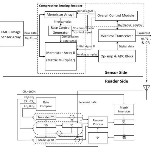
4 Exploiting Memristor in CS Application, Part II Circuit Implemen-tation 50 4.1 Memristor based CS Encoder Design . . . 52
4.1.1 System architecture . . . 52
4.1.2 Memristor array for CS . . . 55
4.1.3 Sparsity estimator . . . 58
4.1.4 Implementation . . . 61
4.2 Evaluation . . . 64
4.2.1 System hardware and power analysis . . . 64
4.2.2 A case study . . . 66
4.3 Chapter Summary . . . 71
5 Exploiting Memristor in CS Application, Part III Recovery Algo-rithm Enhancement 72 5.1 Compressive Sensing With Prior Samples . . . 73
5.2 Utilizing Fully Connected Neural Network for Weight Predictions . . 74
5.2.1 Preliminary of FCNN . . . 74
5.2.2 Utilization of FCNN . . . 75
5.3 Updated CS Overall System Architecture . . . 76
5.3.1 Overall System Blocks . . . 76
5.3.2 CS Sampling through Memristor Array . . . 79
5.4 Prediction-based Orthogonal Matching Pursuit . . . 80
5.5 Evaluation . . . 87
5.5.1 Analysis of PrOMP Algorithm . . . 87
5.5.2 Analysis of Neural Network Prediction . . . 88
5.6 Chapter Summary . . . 90
6 Conclusion and Future Work 91 6.1 Conclusion . . . 91
6.2 Future Work . . . 92
List of Figures
2.1 Matrix multiplication based sampling process of compressive sensing . 11 2.2 Updated sampling process with sparse coding (transformation) . . . . 12 2.3 Existing implementation of compressive sensing in digital CMOS circuits. 17 2.4 Concept figure of memristor device . . . 22 3.1 (a) The proposed memristor-based compressive sensing system; (b)
Memristor array for implementing random sensing matrix. . . 26 3.2 A generic P t/T iO2/P t memristor device: top is the conductive
fila-ment growth model and bottom is the illustration of filafila-ment length and device resistance. “C” stands for cathode and “A” stands for anode. 30 3.3 The energy band structure of T i2O3/T iO2/P t wire: s1 is the left-side
boundary to the actual barrier, s3 is the right-side boundary to the actual barrier, and s2 =s−s3. . . 34 3.4 Ohmic model with tunneling effect. . . 34 3.5 Memristor conductance under (a) different writing time and (b)
differ-ent filamdiffer-ent lengths. The vertical axis indicates the normalized con-ductance, i.e., LRS (on-state) has a value of 1 and HRS (off-state) has a value of 0.001. . . 38 3.6 Variations versus average filament length under different conditions:
(a) variations are introduced to each parameter separately; (b) varia-tions are introduced simultaneously for all three parameters; and (c) comparison between (a) and (b). . . 39 3.7 Distributions of memristor array conductance with filament length at
different regions: (a) “No Turn-on” (4nm), (b) “Limited Turn-on” (9nm), (c) “Lots of Turn-on” (12.7nm), and (d) “All Turn-on” (13nm). 40 3.8 (a) Mean square errors at different filament lengths; (b) Peak
signal-to-noise ratios at different filament lengths. . . 45 3.9 Recovery results of “Lena”. . . 46 4.1 The overall system block diagram. . . 53
4.2 Memristor array arrangement for CS. . . 55 4.3 Integration of the proposed CS encoder with the traditional image sensor. 57 4.4 Memristive segment adder. . . 58 4.5 Compressed rate controller. . . 59 4.6 Detailed implementation of the proposed CS encoder. . . 61 4.7 Flow chart of encoder operations for (a) initialization process and (b)
normal operation. . . 62 4.8 Examples of the recovered frames through the proposed system. . . . 69 4.9 Examples of recovered frames of a fixed compressed rate system. . . . 69 4.10 PSNR results. . . 70 5.1 A simple example of fully connected neural networks . . . 75 5.2 Fully connected neural networks utilized in the proposed design . . . 75 5.3 The overall system block diagram . . . 77 5.4 Memristive Compressive Sampling Module with Prior Samples
Acqui-sition . . . 78 5.5 Weighs predictions after iterative initialization . . . 87 5.6 Recovery performances of proposed PrOMP versus AMP, where N =
256, M/K = 128/64 . . . 89 5.7 Historical Statistics of different error rate per input block . . . 89
List of Tables
3.1 Mutual Coherence at Different Switching Regions . . . 44
3.2 Recovery Performance under Different Setups in DCT Domain . . . . 47
4.1 Notation declaration of the proposed design . . . 52
4.2 Functions of switch sets S1 – S6 . . . 63
4.3 Specifications of the hardware platform for simulations . . . 65
4.4 CS encoder implementation and power analysis . . . 67
4.5 Notation declaration of power saving equations . . . 67
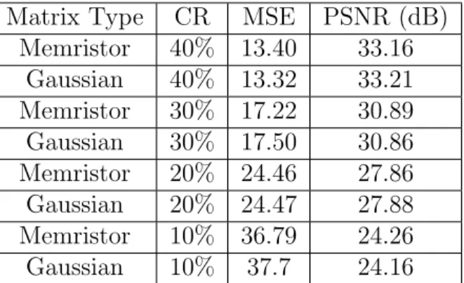
4.6 Comparison of signal reconstruction quality . . . 68
4.7 Comparison of System Energy Savings for Different Numbers of TX Antennae . . . 71
Chapter 1
Introduction
1.1
Background
Compressive Sensing (CS), also named as Compressed Sensing, is proposed about a decade ago [12], and still gaining intensive attention in recent years. Sub-Nyquist sampling rate and low complexity sensing architectures are contributes to its major features, which make it very promising during the applications where resources are restricted, such as mobile devices, robotic system, wireless sensor networks (WSNs), and Internet of Things (IoT). With most of these applications, data compressions are applied to sensory signals through CS technique for power efficiency improvement. Among different sensory applications, image sensor with video streaming applications attracts most of our interests because of the ever increasing usage and huge data volume involved. It can benefit a lot if CS process can be integrated into the imagery system.
sys-tems, and artificial intelligent (AI) applications such as face identification, self-driving cars, and robotic systems. Furthermore, with the growing usage of cloud comput-ing, wireless or wired video streaming is becoming more and more important. The power consumption of image sensors in video streaming, usually at gigabyte-per-second rates, is around watt level [21]. A lot of energy and resources can be saved during data processing and transmission if source data can be compressed. To achieve this goal, an effective approach is needed to cut down the dimensions but preserve enough information of the original input data. Traditional codec methods such as JPEG, H.264/MPEG4-AVC are post-sampling approaches; they could not provide improvement at the sampling stage (e.g. the operations of ADC). Furthermore, they will introduce large complexity and energy consumption because of the intense arith-metic operations. For example, the power of a H.264 module is hundreds of milli-watt [39]- [15] [70].
Therefore, the major work of this thesis study is to design the replacement of traditional data compression solution via compressive sensing technique for sensory signals, and applied the circuitry implementations to practical video streaming sys-tem. However, there are several bottle-necks of compressive sensing technology, which are also related to the motivation of this thesis and will be explained in details with Chapter 2.
On the other hand, memristors as a new class of nano-electrical devices have gained significant attention in both academia and industry in recent years. Memristor devices can be utilized in two ways: digital circuits that exploit high resistance off-state (HRS) and low resistance on-state (LRS) to achieve binary logic, and analog circuits that operate on continuously changing resistance values. Compared to CMOS transistors, memristors feature many unique properties, such as reversible voltage controlled
re-sistance, high operating speed, high density, and non-volatility [62]. Extensive studies have been carried out in designing and implementing high-density data storage [16], analog computing and neural networks [1], advanced robotic control systems [2], [3], and hardware security [25] [26], by utilizing the intrinsic characteristics of memristor devices.
Although memristors have a great potential for use as the essential components to build future memory and computing systems, it is still quite challenging to inte-grate these devices at a large scale. One limitation is the variation effects stemmed from device fabrication processes. For example, when a typical “electrode/metal-oxide/electrode” memristor device is fabricated through the establishing processes such as lithography and vapor deposition, there exist numerous uncontrollable fac-tors that inevitably introduce non-ideal artifacts into the fabricated devices, which in turn result in significant uncertainties in device behaviors. It is extremely difficult, if not impossible, to maintain the uniformity among the fabricated memristors. Even the same memristor may exhibit inconsistent properties under different operating conditions. Moreover, small fabrication fluctuations could trigger large state varia-tions, which will affect the signal integrity of digital or analog circuits implemented by memristors. Most existing work on memristor-based systems either do not give sufficient consideration to these non-deterministic effects, or assume these effects can be minimized without accounting for the incurred cost or design overhead.
To reap the benefit of memristors, a new research area emerges that deliber-ately exploits fabrication variations in memristors for functions where randomness and uncertainties are appreciated. It has been reported that the stochastic behaviors of memristors can be leveraged to design light-weight true random number gener-ators [68] and physical unclonable function (PUF) [44]. These works open a new
direction to fulfill the promise of memristors under the state-of-the-art fabrication processes. And based on the study of this dissertation work, we find out that both CS and memristor device can benefit from each other during the design area where memristors are exploited for compressive sensing applications. With the existence of process variation, memristor units can be utilized as the random sensing matrix for CS application. Meanwhile, CS system will be more power efficient and accelerated through memristor enabled analog computing.
At the early steps of this dissertation work, we considered the power consump-tion problem of convenconsump-tional CS implementaconsump-tion. Addiconsump-tionally, memristor is utilized in our former work as true random PUF [44]. Therefore, we believe memristor is a very good candidate for CS application not only for analog computing but also for random number generation (RNG), and we studied the memristor physics with process variation and the feasibility being utilized in CS application [55] [56]. Af-terwards, we selected video streaming and designed the prototype of CS sampling circuit [57]. Then we faced the compression rate control problem when we want to build a comprehensive system to deal with practical CS video streaming application. We solved this problem through well applying memristor device also within control logic for low-overhead and fast pre-sampling [59]. Next, we’d like to further improve our propose CS system with higher compression ability. We chose prior information based approach and updated our CS system so that it can extract prior information from highly compressed samples obtained by memristor array. Furthermore, we also proposed our own prior algorithm to process real prior information which is usually inaccurate. This part is still on-going and will be published in the future work.
As the short conclusion, in this thesis work, memristor device is exploited for compressive sensing application with following usage. The outlines of this dissertation
is presented in the next section, and summarized contributions are afterwards.
• Generation and storage of random matrix for the sampling process, and refresh could be very low-frequent due to non-volatility.
• Applying analog computing to speed up intensive matrix based arithmetic op-erations in CS sampling process.
• Obtaining the estimations of current input sparsity to real-timely adjust com-pression rate for performance optimization.
• Helping to extract prior information of current input to cut down the necessary measurements and also enhance the recovery process.
1.2
Outline of the Dissertation
The remaining of this dissertation is organized as follows:
In Chapter 2, preliminaries of compressive sensing theory is reviewed, including the CS mathematics and basic recovery algorithm. The bottle-necks of CS as our addressing points are also presented. Afterwards, the background of memristor device is introduced.
In Chapter 3, the concept system architecture of exploiting memristor in CS sen-sory applications is firstly explained. Then the physical model and switching process of memristor device under fabrication variation are proposed to study the feasibility of utilizing memristor for CS. Models and optimal switching strategy are evaluated by simulations as well as an graphic case study included.
In Chapter 4, a comprehensive CS system for wireless video streaming is proposed, focusing on the circuit implementation of CS encoding process. The rate control problem is solved by real-time sparsity estimation and matrix reconfiguration, also based on memristive computing. Hardware and power of the proposed system are analyzed in the chapter evaluation section, as well as a case study with practical video data. The comparison between proposed CS system and related H.264 system is also included.
In Chapter 5, prior algorithm is utilized to improve the CS process so that fewer measurements are required in the sensor node and good recovery quality can be still achieved on the receiver side. The proposed CS video streaming system in Chapter 4 is updated and equipped with neural network to extract prior information from mem-ristive samples. Furthermore, a prediction based greedy algorithm is proposed by us to recover the compressed signal with better performance.
The overall conclusion and future work are addressed in Chapter 6.
1.3
Contributions of the Dissertation
The major contributions of this dissertation and related publications are as follows:
• To the best of our knowledge, this dissertation is the first article to list the bottle-necks of compressive sensing technique in terms of system implementa-tions.
• The memristor analytical model presented in this dissertation is the first model which relies on actual physical process and tunneling effect, instead of applying window function or experiment data fitting in traditional memristor models.
• With analytical model, memristor randomness due to process variation are stud-ied in this dissertation. Apart from conventional geometry parameters, the an-nealing related parameters are also included in the statistical analysis as the first time with memristor device.
• This dissertation and our related works are the first time to use memristor ar-ray in analog type for compressive sensing application. Both Gaussian random matrix generation and matrices multiplication are conducted by analog memris-tor array. Guided by the reconstruction performance, the optimized switching strategy is proposed.
• This dissertation develops a comprehensive system architecture for CS video streaming application. Hardware implementation and power analysis are in-cluded and compare with H.264 technology to demonstrate the advances of our proposed system.
• To exploit the system real-time prior information, which are usually with errors and mis-predictions, a new orthogonal matching pursuit algorithm is proposed in this dissertation to pre-process the prior information before recovery itera-tions. By means of that, the necessary number of measurement is decreased so as to the power consumption, and the overall performance is improved.
1.4
Related Publications
Journal papers that are accepted and published with primary authorship include [58] [56] [59]: 1. F. Qian, Y. Gong, G. Huang, M. Anwar, and L. Wang, “Compressive
Sens-ing ExploitSens-ing Real Prior Information,”IEEE Signal Processing Letters (SPL), 2019, under review..
2. F. Qian, Y. Gong, and L. Wang, “A Memristor-Based Compressive Sampling Encoder with Dynamic Rate Control for Low-power Video Streaming,” ACM Journal on Emerging Technologies on Computing (JETC), accepted 2019.
3. F. Qian, Y. Gong, G. Huang, M. Anwar, and L. Wang, “Exploiting memristor for compressive sampling of sensory signals,” IEEE Transaction on very large scale integration systems (TVLSI), vol. 26, no. 12, pp. 2737–2748, 2018.
Conference papers that are accepted and published with primary authorship in-clude [55] [57]:
1. F. Qian, Y. Gong, and L. Wang, “A Memristor Based Image Sensor Exploiting Compressive Measurement for Low-Power Video Streaming,” In Circuits and Systems (ISCAS), 2017 IEEE International Symposium, Baltimore, US, May. 2017, pp. 1–4.
2. F. Qian, Y. Gong, and et al, “A memristor-based compressive sensing architec-ture.,”Nanoscale Architectures (NANOARCH) IEEE/ACM International Sym-posium, 2016
Journal papers that are accepted and published with co-authorship include [26]: 1. Y. Gong, F. Qian, and L. Wang, “Design for Test and Hardware Security
Utilizing Retention Loss of Memristors,” IEEE Transactions on Very Large Scale Integration (VLSI) Systems, vol. 27, no. 11, pp. 2536–2547, 2019.
1. Y. Gong,F. Qian, and L. Wang, “A Secure Scan Chain Test Scheme Exploiting Retention Loss of Memristors,” inIn Circuits and Systems (ISCAS), 2017 IEEE International Symposium, Baltimore, US, May. 2017, pp. 1–4.
Chapter 2
Preliminaries
In this chapter, the preliminaries of compressive sensing theory will be firstly in-troduced, including the sampling process and two fundamental recovery algorithms. Afterwards, bottle-necks of current CS implementations will be quickly reviewed, so as to derive the motivations of this thesis paper. To address these problems, emerging non-volatile memory memristor is exploited in our design. Therefore, the background of memristor device is also presented in this chapter.
2.1
Basics of Compressive Sensing Theory
There exist sparse type of signals in both natural or man-made sources. The word “sparse” means that only limited number of elements in signal sequence are non-zero or significant. Based on some certain algorithm, those zero or insignificant elements can be removed during the storage or transmission to save space or power consump-tion, while the original signal will still be able to reconstructed perfectly or with
Figure 2.1: Matrix multiplication based sampling process of compressive sensing
limited loss when necessary. Compressive sensing (CS) is one of this kind of algo-rithm, which attracts intensive attentions since it is suitable for different applications. In CS applications, sampling process operates at the sensor nodes, and signal reconstruction is computed at the receiver side. Usually, the sensor nodes is resources restricted, thus it is meaningful to compress the input data as much as possible for reliable performance. In this section, the preliminaries of CS are reviewed.
2.1.1
Sampling Process
Compressive sensing is the process of data sampling and compression at the sensor node, and signal reconstruction at the receiver side. The most compelling feature of this technique locates at the simple algorithm and structure within the sampling part, or called measurements acquisition instead, which makes it a very promising technology for the scenarios where resources are restricted. Mathematically, this measurement operations can be expressed as:
Figure 2.2: Updated sampling process with sparse coding (transformation)
where X ∈ RN is the input signal, Y ∈
RM is the compressed measurements, Φ∈RM×N is the sensing matrix, and noi∈
RN represents the sampling noise which is usually the Gaussian white noise. This process is also depicted in Fig. 2.1 with detailed size informations illustrated. By means of this implementation, original data dimension N is reduced to M, where M < N. If the following conditions are met, there is a large possibility to recover X fromY without any data distortion.
First of all, the input signal should be sparse, either by itself or projected to different domains. For another word, it has redundant information so it’s compress-ible. Varies kinds of signals fulfill this requirement, such as image data after Discrete Cosine Transform (DCT) or Wavelet Transform, ECG data, and radio data during wireless communication [61]. Sometimes, the input source cannot achieve the required sparsity level with an existing transform. A learned transformation can be obtained through learning the patterns of data source thus the sparsity level can be optimized by applying it. This area of studies are called dictionaries learning (or sparse cod-ing) [42], applied not only in CS scenario, but also in machine learning aspects. With the transformation process involved, CS sampling process is extended as Fig. 2.2. However, the actual transform operations can be bypassed at the sensor node, where resources are limited, for better energy efficiency. For more specific, let’s assume the
actual implementation is based on Fig. 2.1 while the sparse coding is
Xsparse = Ψ·X, and X = Ψ−1·Xsparse (2.2)
where Xsparse represents the sparse coefficients when X is operated by transform matrix Ψ. Afterwards, Equation. 2.1 is modified as:
Y = Φ×Ψ−1·Xsparse+noi= Φ0×Xsparse+noi and Φ0 = Φ·Ψ−1
(2.3)
During the recovery process, Xsparse can be reconstructed through Φ0 and original input can be calculated accordingly. Based on the above procedures, the computing overhead of Ψ is transfered to the receiver side, where resources are not restricted.
The second condition of CS is placed by the sensing matrix Φ, which should meet the independent and identically distributed (i.i.d.) property, such that it can preserve the original signal after sampling. Further more, this condition is summarized as restricted isometry property (RIP) [11]. A matrix Φ is said to satisfy the RIP if there exist a constant 0< δK <1 which follows the equation below:
(1−δK)||X||22 ≤ ||ΦX|| 2
2 ≤(1 +δK)||X||22 (2.4)
where || · ||2 denotes the operation of pursuing l2-norm. Within actual CS applica-tions, Bernoulli or Gaussian matrices are usually chosen to build the measurement matrix. Inside a Bernoulli matrix, all the elements are either “+1” or “−1” with equal possibility. And in a Gaussian matrix, all the elements follow the normal dis-tribution N(0, σ2). In recent years, learning based matrix formation method [28] is
reported to maximized the i.i.d. property of random matrix, and the related CS performance is improved.
Moreover, there exist studies which focus on utilizing the supplemental materials of input signals within the reconstruction process. These supporting knowledges are called prior information, which could be hypothetical data structure for specific data type, positions of non-zero elements, weights to represent amplitude of input vector, or statistical probability of non-zero spot. Through exploiting prior information, it is proven that the RIP condition will be relaxed and fewer measurements will be required for the restoration of input signal. This dissertation also includes the corresponding work exhibited in Chapter 5.
2.1.2
Recovery Methods
Since M < N, there exist infinite solutions of X that satisfy equation 2.1. Two major algorithms are introduced in this section, and they’re Basis Pursuit (BP) [14] and Orthogonal Matching Pursuit (OMP) [30]. Other reconstruction approaches are Iterative Hard Thresholding (IHT) [7], dictionaries learning [42] and Bayesian based method [33]. Based on the basic concepts of these methods, improved version are proposed for better recovery performance.
Basis Pursuit
It’s proved that the recover of original X should have the smallest l0-norm among those infinite sets. This is calledl0-norm optimization method. However, exhaustive search is needed to solve this problem which makes it a Non-Polynomial (NP) hard problem [49]. Therefore, researchers searched for other approaches to replace this
inefficient method for compressive sensing application. One of them is l1-norm opti-mization, also called Basis pursuit method, where the originall0 argument is relaxed as:
arg min ˆ X
||Xˆ||1, s.t. Φ×Xˆ =Y (2.5) where || · ||1 stands for the summation of all the absolute value of vector elements. This recovered method is utilized in Chapter 3 and Chapter 4, where the design focus locates at the sensor side. Please refer to [9] for detailed algorithm of BP recovery process. In Chapter 5, our improved version of OMP is presented thus the basic idea of OMP will be explained in detailed as the next part of this subsection.
Orthogonal Matching Pursuit
l1 method is said to has the least recovery error under RIP restriction, compared to other alternative solutions. However, its computational complexity and process-ing time still remain very high. Orthogonal Matchprocess-ing Pursuit is a kind of greed algorithm [40], which is famous for achieving high speed signal reconstruction. It is summarized as Algorithm 1.
Algorithm 1 Orthogonal Matching Pursuit (OMP)
Input: Sensing matrix Φ, Measurements Y, and sparsityK Initial residualr0 =Y, and selected support vector S=∅
for i= 1,· · · , K do
Calculate arg maxj|< ri−1,Φ
j >| and find the index j Absorb j into selected support S: Si =Si−1∪j
Signal Update through: ˆXSi = arg minXˆ ||ri−1−ΦS·Xˆ|| Update residual: ri =ri−1−Φ
S·Xˆ
end for
The core idea of OMP algorithm is to find out the index of non-zero element and calculated the updated ˆX through iterations. For more specific, at each iteration, inner products of sensing matrix Φ and residual r are calculated to locate the coor-dinate j where Φj is the most correlated to current residual, and Xj has the largest amplitude among the remaining uncalculated elements. This inference requires the CS process fulfill the RIP condition, otherwise computed j may lead to some zero element as error result.
After the selected j is absorbed into the support S, ˆX is solved by least square methods [8]. However, high computing complexity of least square process restricts the reconstruction speed of OMP algorithm. Decomposition methods such as Cholesky [18] are used to replace the original process for more faster speed. Our previous work [30] also proposed a matrix inversion by-pass technique to improve the OMP performance. Besides, studies also focus on replacing the actual sparsity knowledge K with some certain stopping conditions asK is always unknown during the real applications.
2.2
Bottle-necks of Conventional Compressive
Sens-ing Techniques
It has been more than a decade since compressive sensing theory is proposed. How-ever, the utilizations of CS in real applications and commercialization process are restricted by several drawbacks. First of all, although the implementation of CS sam-pling process is simple, its recovery process involves a lot of iterative matrix based calculations, which limit the entire processing speed. In recent years, researchers are trying to get break-through over this problem via replacing tradition iterative method by neural network implementations [32] [72], called non-iterative approaches. Since
Figure 2.3: Existing implementation of compressive sensing in digital CMOS circuits.
neural network has the ability to learn specific patterns, it has good CS applications in image processing area. Apart from this problem, other critical draw-backs are introduced in this section. The motivation of this dissertation is to address these bottle-necks of CS and propose a comprehensive CS system which is optimized and targeting practical applications.
2.2.1
Power Consumption
Existing CS implementations are either based on optical platform or conventional digital CMOS circuit, having the problem of high power consumptions within the sensor side. This drawback usually limits the potential of CS when applied to the resources restricted scenarios, such as mobile device, wireless sensor networks (WSNs) including image sensor application, and Internet of Things (IoT) networks.
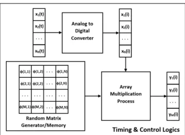
Figure 2.3 shows the generic structure of a digital CMOS-based data acqui-sition system for compressive sensing. It consists of three functional blocks: an
analog-to-digital converter (ADC) that converts N-dimension analog input signals X1(t), X2(t),· · · , XN(t) into digital signals X1(i), X2(i),· · ·, XN(i); a memory block to store the random sensing matrix Φ ∈ RM×N; and a matrix multiplication block that performs compressive sampling and generates outputs Y1(i), Y2(i),· · · , YM(i) (see 2.1).
There are two issues related to power consumption. First of all, the ADC process. During the CS sampling with traditional implementation, all the elements of input signal are required to be converted to digital bits. For another word, the ADC process doesn’t benefit at all from CS application. However, the major power consumption inside an image sensor is cost by the ADC modules [34]. A lot of energy can be saved if the ADC process is adjusted after the input signal is compressed by CS technique. Secondly, implementing matrix multiplications in digital CMOS circuits is costly. As shown in Fig. 2.3, after theith ADC sampling, the length-N signalsX
1−N(i) need to be multiplied with each row of Φ (if a Gaussian sensing matrix is used) and the intermediate results are accumulated to generate one element in Y. This procedure has to be performed on all the M rows of Φ to generate Y1−M(i). Although various techniques [51], [52] have been proposed to optimize matrix multiplications in digital CMOS circuits, the hardware complexity remains high and power/performance may still be stressed to meet the requirement of high-demanding applications such as video processing. Due to this consideration, most digital implementations of compressive sensing use binary Bernoulli sensing matrices to take advantage of simple addition operations. However, the accumulation operations are still costly if the value of N is large. Also, the quality of signal recovery is inferior to that using Gaussian sensing matrices. Hence, there is a need to investigate new hardware solutions that improve the performance of compressive sensing for real-time applications under strict
power/resource constraints. A new compressive sensing architecture is proposed based on emerging device with analog computing in Chapter 3.
2.2.2
Compression Rate Control
As mentioned above, we focus on video streaming as our target application. Video processing are usually based on some block-wise methods [23] to manage computa-tional complexity. In compressive sensing application, frame (image) input is divided into different smaller blocks and compressed individually. That’s because the com-puting complexity is proportional to the order ofN2. The hardware resources of both sampling and recovery process are not affordable if the actual CS input is too large.
The compression rate is usually unknown during the practical applications. There-fore, the compression rate control for each input is usually a problem. And the above block-wise operations amplifier the complexity of this problem. For more specific, different blocks usually have different sparsity conditions, and thus how to manage the compressed rate real-timely for various blocks is the highlight part of a CS design. Some of the existing works apply a fixed upper-bound compressed rate to all blocks [24] for a relatively simpler control logic, but the efficiency is low and recovery quality is negatively affected. During the practical CS applications, some of the blocks can be regarded as background where the corresponding input is quite sparse; while some of the blocks represent fast motion part and no data compression should be applied on these blocks. Another kind of approach [13] relies upon a rate control mechanism based on the result of real-time frame recovery, but the related operations are complicated as well as the requirements of fast recovery speed and low control latency. Therefore, investigating new solutions for block-based CS systems is also
needed, especially under strict power/resource constraints. A CS video streaming system with self-adaptive rate control is proposed in Chapter 4.
2.2.3
Compressing Ability
Through applying CS technique to video streaming, original frames will be compressed to smaller data size for transmitting or storing, leading to the improvement of power consumption at the sampling side. However, another major bottle-neck of CS is lower compression ability compared to traditional video codec methods, like H.264/H.265, MPEG4 or MP4. CS needs more measurements for decent signal reconstructions, following the equation below:
M =O(K ·log(N
K)) (2.6)
where M is the number of measurements, N and K represents the data size and sparsity level of the input signal respectively, andO(·) is the notation expressing that the sufficient measurements is related to the number of non-zero elements, usually in terms of multiple times. However other technology, like H.264, is based on accurate pixel operations and can achieve around sparsity level data compression. Comparison between CS compression and H.264 technique will be given in Chapter. 4. Briefly, to compress a surveillance video with 7% sparsity level, the compressed rate (CR) of CS is about 26% while H.264 can achieve 7.1% for same level of recovery quality.
If sufficient CS measurements can be further cut down, large power consumptions can be saved in practical applications. A lot of studies focus on the research of this problem, and propose different kinds of approaches, such as dictionary leaning and
sparse coding [42], sensing matrix optimization [28], and prior algorithm [47]. Among them, prior method attract more interests from us because of its high efficiency on cutting down necessary measurement amount. For example, if all the positions of non-zero element of X are known to the recover process and included in the support set S, X is decrease to XS with the size of K which equals to the sparsity. The sufficient samplings could be YS also with K element. XS can be solved through least square method with selected columns from Φ (ΦS), and the measurement size is decreased to the level of sparsity. However, acquiring and applying this kind of prior information to CS application will still have some practical problems and will be addressed in Chapter 5.
2.3
Preliminaries of Memristor Device
To address the above bottle-necks, memristor devices are utilized to accelerate the matrix computation, simplify the rate control logic, and help to acquire prior infor-mation. Contributed by its ability of analog computing, matrix multiplication and vector summation can be finished within one clock cycle, and novel system design can be achieved through exploiting this kind of device.
There used to be three basic circuit elements: resistor, capacitor and conductor, while an estimation of the fourth element was made almost 50 years ago by Prof. Chua, which is called the “missing circuit element” [17]. Based on theoretical deriva-tions, the resistance of this device can be tuned to maintain different state and utilized as memory unit, so it is named as memristor. It was actually “found” (fabricated) by HP Lab in 2008 [65].
Figure 2.4: Concept figure of memristor device
As illustrated in Fig. 2.4, a memristor device typically has a sandwich structure with two metal electrodes at each end and a stack of functional nano-material in the middle. Different materials can be used as the functional part, such as binary metal oxide (e.g. T i0x, Hf Ox, ZnOx), chalcogenides (e.g. Ag2S, Cu2S, GexSx), and complex perovskite oxides (e.g. SrT i0.75Sn0.25O3, LaM nO3, BiF eO3) [29]. Consider a classicP t/T iO2/P ttype memristor. When a positive or negative voltage is applied over the electrodes, Titanium material will convert between T iO2 and T i2O3, which are insulator with high resistivity and conductive material, respectively. Based on this mechanism, memristor devices are able to switch between the high resistance state (HRS) and the low resistance state (LRS), which can be utilized for realizing binary logics. These devices can perform analog computing since continuous switching between the two states is also possible.
matrix multiplication is quite simple and straightforward. This structure has already been studied with neural networks and machine learning applications [20]. However, memristor device is fabricated through the establishing processes such as lithography and vapor deposition, there exist numerous uncontrollable factors that inevitably introduce non-ideal artifacts into the fabricated devices, which in turn result in sig-nificant uncertainties in device behaviors. It is extremely difficult, if not impossible, to maintain the uniformity among the fabricated memristors. Even the same memristor may exhibit inconsistent properties under different operating conditions. Moreover, small fabrication fluctuations could trigger large state variations, which will affect the signal integrity of digital or analog circuits implemented by memristors. Most existing work on memristor-based systems either do not give sufficient consideration to these non-deterministic effects, or assume these effects can be minimized without accounting for the incurred cost or design overhead.
As mentioned in preliminary section, sensing matrix Φ needs to be sufficient ran-dom, so we adopted the cross-bar structure and exploited it into the compressive sensing application for both random matrix generation and matrices multiplication. More details of memristor devices physics, switching mechanism and process variation analysis will be explained in Chapter 3, and simulation based evaluation will be also included.
2.4
Chapter Summary
In this chapter, the mathematical theory and algorithm of both compressive sampling and reconstruction are explained in details. Afterwards, different bottle-necks of
current CS implementations are reviewed separately. These problems can be also regarded as the motivation part of this dissertation work. Based on our solutions to them, emerging non-volatile memory memristor is exploited to optimize the CS design. Therefore, the background of memristor device is also included in this chapter.
Chapter 3
Exploiting Memristor in CS
Application, Part I Theory
Investigation
As mentioned in last chapter, exciting CS builds are relied on optical platforms or conventional CMOS circuit. Optical CS setups are mainly with in-lab condition since they are not convenient to be integrated at actual application. However, current CMOS CS implementations still suffer from high power consumption (see Chapter 2). Memristor devices are utilized all over this thesis work to help with the improvement and optimization over CS implementation. In this Charter, the memristor physics with process variation and switching mechanism are studied for pursuing the feasibil-ity of exploiting memristor in CS application. To the best of knowledge, our related publication [56] is the first article of deriving the memristor switching model with tunneling effect based on actual physical process, instead of applying window func-tion or experiment data curve-fitting. An image based case study is also presented
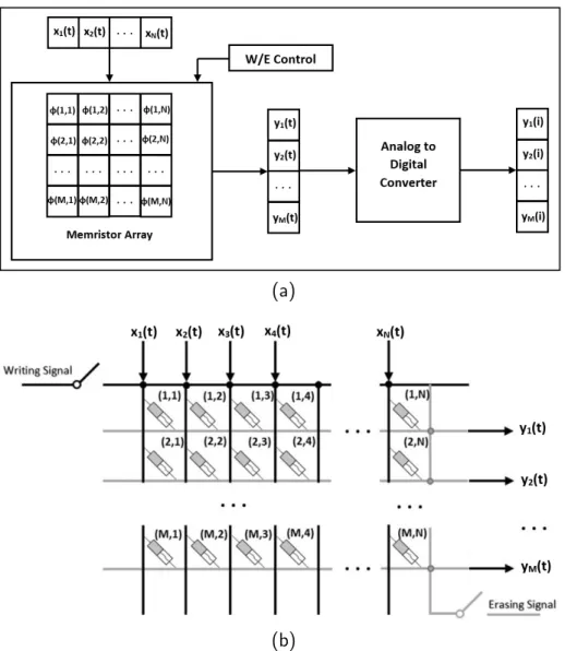
(a)
(b)
Figure 3.1: (a) The proposed memristor-based compressive sensing system; (b)
Memristor array for implementing random sensing matrix.
in this chapter to demonstrate the performance of replacing pre-build sensing matrix with memristive embeddings.
3.1
Proposed Basic System Architecture
To address the mentioned power consumption problems, we propose a new memristor-based design, which allows us to perform compressive sensing in the analog domain with low hardware complexity, fast sampling speed, and high energy efficiency. The proposed memristor-based system is shown in Fig. 3.1a. It includes two functional blocks: a memristor array and an ADC module to sample the output analog signals. The memristor array realizes the random sensing matrix Φ by leveraging the inher-ent randomness in memristor devices due to fabrication variations. Since memristor devices support continuous values, analog Gaussian sensing matrices can be imple-mented to achieve high-quality signal recovery. As compressive sensing is performed in the analog domain, the number of the ADC bits can be greatly reduced from CMOS-based systems, as the dimension of output signals is reduced to M << N.
Before the sampling process starts, an initialization is needed through writing the memristor array with a certain voltage and pulse duration. The random sensing matrix is thus created as it is extremely difficult to maintain the uniformity in mem-ristor devices, in particular if the size of the array is large. A detailed model of this randomness will be discussed in the next section. After the initialization, memristors will be operated at the normal mode and due to the non-volatility of memristors, the initial values will be maintained for subsequent operations. To overcome the undesir-able drifting effect in memristive material [74], each memristor is read alternatively through a positive pulse and a negative pulse, so that the matrix value is protected. Figure 3.1b shows the operations of the proposed memristor-based compressive sensing system. The input analog signals X1(t), X2(t),· · · , XN(t) (e.g., generated by sensors) pass through the memristor array to generate the output analog signals
Y1(t), Y2(t),· · · , YM(t) simultaneously, such as Yn(t) = N X j=1 φ(n, j)× Xj(t); n= 1, 2, 3,· · · , M, (3.1)
whereφ(n, j)∈Φ is the value of the memristor at the crosspoint of thenth row and jth column. The writing and erasing signals indicate the direction of external voltages to write the matrix values during the initialization process or to erase the array. In a practical circuit, φ(n, j) could be the conductance of the memristor. The input signals X1(t), X2(t),· · · , XN(t) could be the voltage outputs of N different sensors, and Y1(t), Y2(t),· · ·, YM(t) are the current signals after compressive sensing. Thus, the above expression can be recast with an underlying physical meaning as
In(t) = N
X
j=1
φ(n, j)× Vj(t); n = 1, 2, 3,· · · , M, (3.2)
whereXj(t) andYn(t) are replaced byVj(t) andIn(t), respectively. The ADC module will then convert the output signals to a digital format for subsequent processing. Note that Fig. 3.1b is intended to be a generic illustration of the proposed idea, and thus many design details (e.g., ground connections) are omitted.
In comparison with digital CMOS-based implementations (see Fig. 2.3), the costly matrix multiplications are replaced by analog operations, and all the M output sig-nals are generated in parallel by the memristor array. At each crosspoint, the inner product is obtained by applying the input voltage over a memristor to generate a current signal (i.e., no extra multiplication circuits), and all the current signals are added up naturally (i.e., no extra accumulation circuits) to produce the output sig-nal. Furthermore, Gaussian sensing matrices can be implemented by memristors
because memristors can be treated as analog devices with continuous conductance values. As a result, the proposed memristor-based system is able to achieve high-speed and high-performance compressive sensing with low hardware complexity and power consumption.
The randomness of the sensing matrix determines the quality of compressive sens-ing. Variations in memristor devices can be exploited to build random sensing ma-trices naturally. This will be discussed in the next section.
3.2
Model of Memristor Random Sensing Matrix
Memristor devices can be fabricated in different ways, each resulting in some unique properties. Existing models [60] [54] [35] are usually based on curve fittings of exper-iment data via applying window functions on the flux model. The proposed system leveraging process variations for compressive sensing requires a detailed analysis of memristor physical mechanisms at nanoscale. In this section, we will develop a com-prehensive memristive filament growth model for this purpose.
3.2.1
Memristor Physical Model
The randomness in the conductance of memristors make it possible to build the random sensing matrix in Equation 3.1. In this chapter, we will focus on a generic bipolar titanium oxide memristor model. Titanium oxide memristors areP t/T iO2/P t type whose conduction mechanism is shown in Fig. 3.2 for a single cell. The functional material is T iO2 nanowire sandwiched by two platinum electrodes. When a positive bias voltage is applied, chemical reactions occur and turn T i4+ into T i3+ (see (3.3))
Figure 3.2: A genericP t/T iO2/P tmemristor device: top is the conductive filament growth model and bottom is the illustration of filament length and device resistance. “C”
stands for cathode and “A” stands for anode.
by electron ionization near the anode region. Positive charged T i3+, in the form of T i4O52+, start to drift towards the other electrode and react with sneaked O2− ions to generate T i2O3, which is a metastable phase of titanium oxide. Then, T i2O3 is accumulated at the cathode side and forms the highly conductive nanowire called filament, growing towards the anode. In this type of memristors, the conductance G is determined by the length of the filament. In general, a longer grown nanowire reduces the overall resistance. The underlying chemical reactions can be described as: 8T iO2 → 2T i4O2+5 + 3O2 + 4e−, T i4O52+ + O2 − → 2T i 2O3. (3.3)
On the other hand, the reverse reaction of Equation 3.3 occurs when a negative voltage is applied. Thus, the conductance change is reversible. As shown in Fig. 3.2, a high resistance state (HRS) is defined when the filament is still within a short length, whereas a low resistance state (LRS) is achieved after the filament exceeds a certain length. Between these two states is the transitional state, and the filament should be
preset to this region in order to utilize its randomness.
3.2.2
DC Analytical Model
As discussed above, the conversion between the two Titanium materials relies upon electron ionization so that the process of filament growth can be dispersed into the ion drifting iterations. During the initialization process, a positive writing voltage is applied for a limited time. In each iteration, limited ions travel through the nanowire, acting on a cross-sectional deposition of T i2O3. The incremented filament length is a sinusoidal function, which has been derived in our previous work [43]:
ax = 2qVm0∗ × 1 d−(a1+a2+···+ax−1)(sinωtx−1 −sinωtx) − κ 1+(ωτ)2 1 d{(sinωtx−1−ωτcosωtx−1) −(sinωtx−ωτcosωtx)} ×(∆t)2 tx =x×∆t (3.4)
where q and m∗ are the electron charge and its effective mass, V0 is the applied voltage,dis the device thickness which could be the maximum length of the filament, ax stands for the grown length introduced by the xth iteration, ω and τ are the frequency and mean free time, respectively, between two successive collisions of ions and material lattice or impurity, which can be determined by the intrinsic property of titanium, ∆t is the time duration of each iteration determined by the thickness d and material mobility, tx denotes the accumulation time of all the iterations, and κ is given by the Arrhenius equation [43].
Whether the value of ax is positive or negative is related to the polarity of V0. Thus, the filament growth can be considered as an incremental or decremental process of ax, as f i=tswitch/∆t, l= f i X x=1 ax, (3.5)
where f i is the number of growth iterations under the applied constant pulse V0 with a duration of tswitch. After the initialization, a smaller reading voltage will be applied bidirectionally to the device to read its resistance and conductance values without introducing any drifting. With a certain filament length l, the resistance of a memristor can be estimated as
Rcon =RON × dl, Rins =ROF F × 1− dl , Rmem =RON +ROF F, (3.6)
where Rcon, Rins, and Rmem are the resistance related to the conductive T i2O3 filament, the insulated T iO2 region, and the overall memristor, respectively, while RON and ROF F are the resistance of LRS and HRS, respectively.
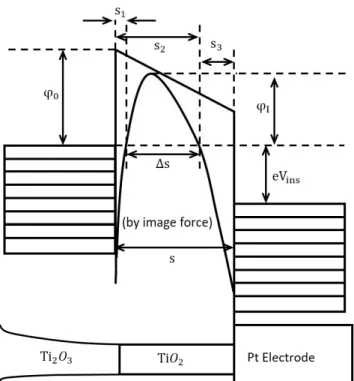
Note that when the insulator barrier is thin enough, electrons can directly go through causing a large current. This phenomenon is referred to as the tunneling effect. At nanoscale, tunneling effect cannot be neglected if the resistance needs to be calculated accurately. Furthermore, the non-linear tilting introduced by the tunneling effect will add more uncertainties to the randomness of memristor devices. Exploiting
the existing work [64], the tunneling effect is added to the proposed model as follows: J = 6.2×10¹⁰ ∆s2 (ϕIe(−1.025∆sϕ 1 2 I)) −(ϕI+Vins)e(−1.025∆s(ϕI+Vins) 1 2) ϕI =ϕ0− (V2inss )(s1+s2)− K(5s.275−s1)lns2(s −s1) s1(s−s2) s=d−l s1 = Kp6ϕ0 s2 =s[1− 3ϕ0Kps+2046−2VinsKps] +s1 ∆s=s2−s1 (3.7)
where J is the tunneling current density under the force of insulator’s overriding voltage Vins, and Kp is relative permittivity of T iO2. Other parameters are defined in Fig. 3.3, e.g.,ϕ0 is the difference of work functions between T i2O3 and T iO2. Note that the above equations have been simplified from their original format. For example, we ignore the difference in the work functions ofT i2O3 and Platinum because both of them are conductors and the difference is small. With the existence of image force [6], the rectangular barrier caused by the Titanium insulator is modified to a parabola shape, which introducess1,s2, and ∆sto depict the barrierϕI under the image force. By summarizing the above derivations, the overall current can be considered as the sum of tunneling current and insulator current, as shown in Fig. 3.4. Then the value of memristor conductanceG can be calculated by solving the following equations:
Figure 3.3: The energy band structure of T i2O3/T iO2/P t wire: s1 is the left-side boundary to the actual barrier,s3 is the right-side boundary to the actual barrier, and
s2 =s−s3.
Im =Itun+Iins Vins =Vm−Im×Rcon Itun=J×A (3.8)
whereIm,Iins, andItun stand for the current flow over the conductingT i2O3 wire, insulatorT iO2 wire, and tunneling introduced current, respectively;Vm is the reading voltage, A is the cross-sectional area of the device, Rcon and J are defined by (3.6) and (3.7), respectively. At the same time,Im is also equal to the overall current. Note that (3.8) can be solved by numerical iteration methods such as binary searching, so that Im can be determined in order to calculate the final conductanceG as:
G= 1 R =
Im Vm
. (3.9)
In summary, the proposed memristor analytical model covers the writing process that generates the filament of length l, and the reading mechanism that evaluates conductance G, with the tunneling effect being accounted for. Furthermore, this parametric model enables us to study the variation process in memristors, as discussed in the next subsection.
3.2.3
Process Variation Analysis
After the initialization stage, the memristors in the array should ideally be reset to the same conductance value. However, the actual conductance values contain variations across different memristor devices. As a result, the entire matrix can be considered as having random numbers. In the analytical model above, the device parameters
that affect the conductance value can be categorized as
• Physical constants such as electron charge q and effective mass m?;
• Material intrinsic properties such as frequency ω related to the lattice size, iteration time ∆t, work function ϕ0 and relative permittivity Kp;
• Device geometry features such as cross-sectional areaAand titanium film thick-ness d.
Physical constants are typically treated as stable values, and most Titanium intrin-sic properties may only contain very small fluctuations due to the defects or impurity inside. An exception is permittivity Kp. Previous work [46] reported that Kp will suffer from large variations due to different annealing processes. This will be taken into consideration in the next section. For device geometry features, variations can be expected from the fabrication process. Although there are different ways to fabricate memristor devices, the general process always contains patterning of electrode array, deposition of Titanium material, and its annealing process. During the fabrication, variations are inevitable at the nanometer range; for example, some fabricated mem-ristor cells have a titanium layer of thickness as small as 10−15nm. Hence, the line edge roughness (LER) in electrode patterning and thickness fluctuation (TF) in the deposition process will occur easily. These hard-to-control factors introduce varia-tions into A and d [50]. Furthermore, annealing is another source of variations that has not been sufficiently studied before. Actually, different annealing temperatures will directly affect device conductivity as well as dielectric constantKp. This chapter will evaluate the randomness caused by these parameters.
All the variation factors mentioned above have cumulative effects, which make it extremely difficult to control the final filament length l and thus the conductance G of a memristor, resulting in large randomness in the memristor array as shown in Fig. 3.1b. While this artifact should be avoided in most applications, it is actually a desirable feature for compressive sensing as required by the random sensing matrix Φ. In the next section, we will utilize the proposed analytical model to study the ran-domness in memristor sensing matrices and identify the optimal switching condition for compressive sensing applications.
3.3
Evaluation of Proposed Random Model
In this section, we evaluate the proposed memristor-based compressive sensing tech-nique. We first study process variations and their impact on the randomness of the memristor array that forms the sensing matrix. Then we assess the signal recovery performance of our approach. A case study of image processing is also provided for validation.
3.3.1
Sensing Array Randomness
The proposed compressive sensing system assumes using a fabricated memristor de-vice [69], which has a 100× 100× 13nm3 geometry structure and 1000 R
of f/Ron ratio. We applied the analytical model (see (3.4)–(3.9)) on the conduction mecha-nism discussed in section IV. Constant parameters were determined by the material properties consistent with the existing work [22]. The memristor devices were first applied a 1.3V writing pulse under various durations for obtaining different filament
(a) (b)
Figure 3.5: Memristor conductance under (a) different writing time and (b) different
filament lengths. The vertical axis indicates the normalized conductance, i.e., LRS (on-state) has a value of 1 and HRS (off-state) has a value of 0.001.
lengths, and then read by a voltage of 0.6V. Under the ideal condition without any variations, the overall conductance of one memristor is shown in Fig. 3.5, with initial filament length equal to zero for simplification. These curves are semi-log type where the on conductance is normalized to 1. Based on Fig. 3.5a, a writing time of 110nsis long enough to fully turn on the memristor. Note that there exists a sharp increase re-gion caused by the tunneling effect. Correspondingly, in Fig. 3.5b, tunneling becomes effective after the filament length is longer than 11.7nm. This is because electrons can only get through the barrier when the insulator gap is thin enough. Although this nonlinear effect takes place when the filament is just 1.3nmaway from its full length, it significantly influences the device performance, which will be explained later.
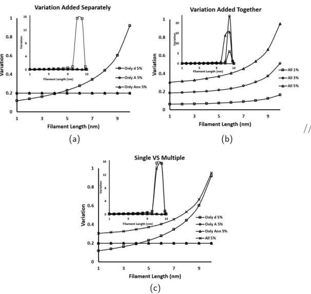
For simplification, we primarily consider thickness, cross section area and anneal-ing variations in the non-ideal fabrication process. Specifically, the memristor is only
(a) (b)
//
(c)
Figure 3.6: Variations versus average filament length under different conditions: (a)
variations are introduced to each parameter separately; (b) variations are introduced simultaneously for all three parameters; and (c) comparison between (a) and (b).
13nmthick so a variation level fordof less than 10% is proper for the practical case. On the other hand, the device cross section area is relatively large, and thus we set the maximum variation as 5% for this parameter. It was shown that different annealing temperatures of Titanium oxide can result in different material resistivity and relative permittivity Kp. The variations of these parameters are estimated as 10% and 5%
(a) (b)
//
(c) (d)
Figure 3.7: Distributions of memristor array conductance with filament length at
different regions: (a) “No Turn-on” (4nm), (b) “Limited Turn-on” (9nm), (c) “Lots of Turn-on” (12.7nm), and (d) “All Turn-on” (13nm).
respectively. Note that we select these maximal variation levels for demonstration purpose. The actually values can be measured from the fabricated devices, which may lead to different numerical results but will not affect the essence of the proposed work.
Different levels of process variations are introduced to the thickness d, cross sec-tion area A and annealing index Ann. The corresponding simulation results are summarized in Fig. 3.6, where the vertical axis represents the variation of memris-tor conductance and the horizontal axis (filament length) is zoomed up to 10nm for
detailed view, and each embedded figure shows the overall curve from 0 to 13nm. Specifically, Fig. 3.6a shows the impact of individual parameter separately on device variations, whereas Fig. 3.6b shows the overall effect of all the three parameters. In Fig. 3.6a, it is easy to see that area and annealing effect introduce a relatively con-stant level of variations, while the influence of thickness is nonlinear. This is because the parameter d exists in the high-order polynomials of the analytical model. From Fig. 3.6b, it is obvious that the overall variation increases with the growth of filament length. Larger uncertainties in these three parameters will certainly increase the over-all variation level. In Fig. 3.6c, where data of individual 5% variations and overover-all 5% variations are illustrated in the same figure, it is evident that the dominant factor in memristor variations is thickness d. Also, memristors with length ranging from 10−12.5nm have larger variations (see each embedded figure), which are caused by the tunneling effect. Under the same writing condition, some memristor devices may have already been fully turned on while the others are still with the filament length located around the tunneling region.
Monte Carlo simulations were conducted to obtain the distribution of memristor conductance. Based on the observation of simulation data, memristors are divided into four groups: “No Turn-on” (average filament length 0−8nm), “Limited Turn-on” (average filament length 8−12nm), “Lots of Turn-on” (average filament length 12−13nm) and “All Turned-on” (filament length ≥ 13nm). These categories also follow the patterns of recovery quality in the next subsection, where we chose 4nm, 9nm, 12.7nm, and 13nmas the representative points for different regions. Histograms of these four groups are shown in Fig. 3.7, and they are within 5% process variations for all the three parameters. The profiles of Figs. 3.7a and 3.7d are quite similar to Gaussian distribution or log-normal type, indicating they are good candidates for
compressive sensing applications. For Fig. 3.7b, only a few memristors, as shown in the embedded figure, are turned on with large conductance and thus this distribution is not suitable for compressive sensing applications. For Fig. 3.7c, except for the conductance below 500mS, memristors follow Gaussian distribution. This case will be proved to be good enough to support compressive sensing applications.
3.3.2
Statistical Analysis of Memristive Compressive Sensing
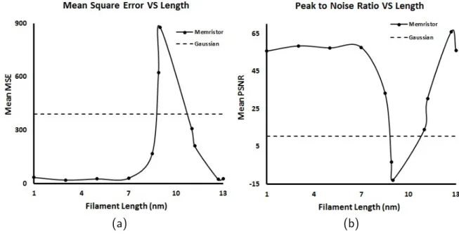
Since memristor conductance values could be random, Monte Carlo tests were per-formed to evaluate the proposed system, including generation of different input sig-nals, memristor array initialization, sampling, recovery and quality assessment. Fur-thermore, simulations based on ideal Gaussian matrices were also conducted under the same conditions for comparison. Measurements were collected from memristor arrays whose filament lengths are tuned to different values, and the resulting compressively sampled signals were recovered by a standard l1-norm algorithm [12]. To quantify the recovery performance, mean square errors (MSE) and peak signal-to-noise ratio (PSNR) are utilized. MSE is defined as:M SE= 1 n n X i=1 (xi−xˆi)2, (3.10)
where xi is the actual ith value of a n dimensional vector (x1, ..., xn)T and ˆxi is its prediction. On the other hand, PSNR is defined as:
P SN R= 20·log10(M AXI)−10·log10(M SE), (3.11)
Generally, a lower MSE or a higher PSNR indicates better quality of the recon-structed signal. For the selected filament lengths, 1000 tests were conducted to obtain the average MSE and PSNR, as shown in Fig. 3.8. There is a performance drop at the range of 8−12nmfilament length, which should be avoided for practical applications. As mentioned above, the entire filament length can be treated as four regions while 8−12nmis the so-called “Limited Turn-on”, whose performance is the worst among all the cases. This is because, as shown in Fig. 3.7b, only a few memristors are tuned to relatively large conductance values and the distribution does not indicate large randomness. For other cases, we can see most of the conductance values are within the similar range.
3.3.3
Optimal Switching Strategy
As revealed in Fig. 3.8, for performance in terms of MSE and PSNR, the worst case is filament length of 9nm, while the best case locates at 12.7nmfilament length. As a result, they are chosen as the representative points for “Limited Turn-on” and “Lots of Turn-on” regions, respectively. The related histogram of the best-case switch-ing (see Fig. 3.7c) is close to Gaussian distribution and the sensswitch-ing matrix Φ has a smaller mutual coherence compared to “No Turn-on” and “All Turn-on”. However, the distribution of the worst case (see Fig. 3.7b) shows little randomness. As shown in [10], [19], a better signal reconstruction can be achieved by a less coherent sensing matrix under the same distribution. Mutual coherence is widely used to quantify the coherence of different columns in the sensing matrix. Since compressive sensing is usually conducted on some sparse transform domains (DCT, DFT, etc.), it is neces-sary to evaluate the mutual coherence of a sensing matrix under different transforms.