J. Micromech. Microeng.15(2005) S39–S46 doi:10.1088/0960-1317/15/7/006
A three-dimensional electrostatic actuator
with a locking mechanism for
microcavities on atom chips
C O Gollasch
1, Z Moktadir
1, M Kraft
1, M Trupke
2, S Eriksson
2and E A Hinds
21School of Electronics and Computer Science, University of Southampton, Highfield, Southampton, SO17 1BJ, UK
2Blackett Laboratory, Imperial College, Prince Consort Road, London SW7 2BW, UK
E-mail: [email protected]
Received 29 November 2004, in final form 1 March 2005 Published 20 June 2005
Online atstacks.iop.org/JMM/15/S39
Abstract
A micromachined three-dimensional electrostatic actuator that is optimized for aligning and tuning optical microcavities on atom chips is presented. The design of the 3D actuator is outlined in detail, and its characteristics are verified by analytical calculations and finite element modelling.
Furthermore, the fabrication process of the actuation device is described and preliminary fabrication results are shown. The actuation in the chip plane which is used for mirror positioning has a working envelope of 17.5µm. The design incorporates a unique locking mechanism which allows the out-of-plane actuation that is used for cavity tuning to be carried out once the in-plane actuation is completed. A maximum translation of 7µm can be achieved in the out-of-plane direction.
(Some figures in this article are in colour only in the electronic version)
1. Introduction
The study of cold neutral atom clouds that are confined in microscopic traps has recently become a very active field of research [1, 2]. The ability to confine and manipulate atoms above micro-structured surfaces—known as atom chips—holds great promise for integrated atom optics and the realization of novel quantum devices such as atom interferometers [3] and quantum information processors [4]. Most atom chip experiments to date, including the first Bose–Einstein condensate on a chip [5], have produced the trapping fields with current-carrying wires. These structures are typically lithographically patterned and remain fixed throughout the experiment. Being able to actuate components on the atom chip would expand the range of devices that can be integrated on an atom chip. One specific example is the optical microcavity, which could make the detection of single neutral atoms on a chip possible [6]. Two key requirements of an optical cavity, alignment and tunability, can be met if the cavity-mirrors can be moved.
X
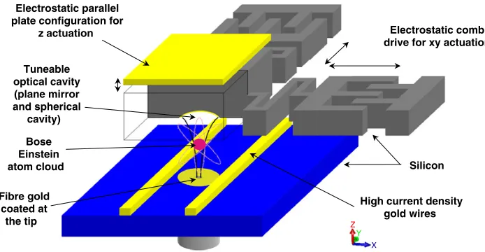
Figure 1.Schematic representation of the atom chip.
with an accuracy in the sub-micron range and a parallel plate configuration for thez-actuation with a maximum translation of 7µm and an envisaged accuracy of a few nanometers. The working envelope of the electrostatic xyz-actuator ensures the required alignment and tunability of the optical cavity. Further, a unique locking mechanism for the xy stage is implemented.
This paper is organized as follows. In the following section we present the general principles of our atom chip. In section 3 we discuss the details of the actuator design based calculations. In section 4 we show simulated results of the movement. Section 5 deals with the fabrication issues of the actuator. Finally, we conclude the paper in section 6.
2. System principles
The layout of the proposed atom chip is shown in figure 1. The chip consists of high current-density gold wires that have been micromachined on a silicon substrate [17]. The wires extend further into a region on the atom chip (not shown in figure 1) where the atom cloud is initially trapped and cooled by standard methods (see, e.g., [2]). The atoms are then guided along the wires into the structure which includes the
xyz-actuator. Here, the high-reflection coated tip of a single-mode optical fibre is mounted between the atom guiding wires. The fibre has two functions; the high reflection coated fibre tip serves as a plane cavity mirror while the fibre itself is used as the input and output port for laser light. A second mirror, that is spherical [18], is fabricated on a platform which is then attached to thexyz-actuator. This assembly is placed opposite the plane mirror at a distance which leads to an optically stable cavity. The alignment and tuning of the optical cavity becomes possible using the actuator. Laser light that is coupled to the optical cavity can then be used to characterize the trapped atom cloud.
A cross section of the atom chip in figure 2 details the three-dimensional actuation structure, with the optical cavity and the optical fibre. Additionally the novel locking mechanism of thexy-actuation is shown which offers improved mechanical stability for the optical cavity tuning.
silicon substrate #4 gold wires spacer wafer #3
z actuation
optical fibre
trapped atoms
xy actuation silicon substrate #2
glass substrate #1 locking
mechanism
Figure 2.Cross section of the multi-layered atom chip actuator.
3. Design of thexyz-actuator
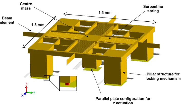
A detailed diagram of the actuator is shown in figure 3. The
xy-plane actuation is accomplished by four individually driven comb structures that are connected via four-beam elements to a centre frame. The spherical cavity is embedded within the centre frame in the serpentine spring suspended centre mass. The movable element of each comb drive is suspended by a double-folded spring suspension with a beam widthw =
3µm and a lengthl1=200µm. The four-beam elements that
connect the comb drives to the centre frame structure have the same width as the spring suspension, but their length isl2=
300µm. This choice of beam width and beam length gives the system a low spring constant which is beneficial for the translational range of the system.
The gap between the comb fingers is g = 3 µm with a height h= 60µm. For a deflection in one direction the translation function is given by [19]
y(V )= ε0N h g ktot,y
V2 (1)
[image:2.595.294.525.295.445.2]Figure 3.Three-dimensional actuator outlining the relevant design parts.
Figure 4.Centre frame structure that encloses thez-actuator. The locking mechanism can be seen in the enlarged view where the silicon oxide stubs (red) are clearly visible.
constant taken as the sum of the spring constant of the double-folded spring in one comb drive and the spring constant of two-beam elements (see figure 3). The motion accuracy of the in-plane actuation is primarily defined by the operation voltage. It is strongly dependent on the gradient of the first derivation of the translation function (equation (1)) and is given by
d
dVy(V )=
d dV
ε0N h
g ktot,y
V2=2mV (2) wheremis the gradient. Due to the quadric character of the translation function, the accuracy is defined by the gradient
m of equation (2). However, the linear approximation of equation (2) is only valid for smallV. Increasing the driving
voltage at 40 V of around 100 mV results in the motion of 5.3 nm at a deflection of 1.05µm. The voltage source used for operation is able to provide a stabilized voltage of around 10 µV. Thus, the analytical resolution of the actuator is not limited by the operation voltage, but rather constrained by external noise such as vibration as well as Brownian noise and intrinsic noise.
[image:3.595.112.465.347.551.2]The system can be unlocked simply by switching off the applied voltage. In order to avoid a discharge between the two electrodes several silicon oxide stubs are processed on the bottom surface of the silicon pillars facing the gold electrodes. The principle is shown in the enlarged view of figure 4. The stubs reduce the contact area between the electrodes which allows the system to unlock without having the contact surfaces sticking together. Applying the locking mechanism to the
xy-actuation is expected to reduce the impact of any external vibration to the entire system, hence improving the stability of thez-actuation.
The parallel-plate configuration that is used for the locking mechanism is also used forz-actuation. With an actuation beyond 1/3 of the initial gap spacing, the system becomes unstable and the pull-in phenomenon becomes effective [21]. In the actuator, the initial gap spacing between the centre mass that is suspended by four serpentine springs and the opposite facing gold electrode on the glass substrate is 21 µm (see figure 4), which then means that the maximum actuation is limited to 7µm. Using equation (3) with the values forkz=
0.652 57 N m−1, g0 = 21 µm and A = 0.04 mm2, the
pull-in voltage for thez-actuation becomes VPI = 71.12 V.
The characteristic of motion accuracy in the out-plane actuation is equivalent to the in-plane actuation accuracy as described above. Hence the same voltage source can be used to tune the optical cavity in thez-direction within a few nanometers.
4. Simulation
During the design evaluation, several simulations on the actuation have been carried out by using finite element modelling (FEM) software to verify the analytical calculations. The results are shown in figure 5, where we plot the simulated
xy-translation curves of the comb drives. Translation curves calculated using equations (1) and (3) have been included for comparison. The translation curve for a deflection which is produced by operating only one comb drive is outlined in blue, while the combined operation of both comb drives is outlined in green. Due to the symmetrical character of the device, the deflection curves are the same in both directions in the
[image:4.595.296.524.64.234.2]xy-plane. Translation curves for thez-actuation are also shown in figure 5. The simulation yields a maximum deflection of 6.77µm at the pull-in voltage of 69.73 V which is within 2%
Figure 5.Translation curves of the actuation. The notationxyis used here to indicate a combined drive along both axes.
Figure 6.Simulation result of a translation of 8.75µm in the +ydirection at 117 V.
of the analytical result. This translation range is sufficient to tune the cavity over several fringes at a wavelength of 780 nm.
Simulation results confirm that for the design with 330 comb fingers for each comb drive, a maximum translation of 8.75 µm of the centre frame in one direction (measured from the origin) can be achieved by applying 117 V to the comb drive. A colour-coded representation of the simulation in the +ydirection is shown in figure 6.
[image:4.595.293.528.279.519.2]Figure 7.Simulated translation of the centre mass in the +yand +xdirection of 11.79µm at 117 V.
(cf figure 5—green graph). A comb drive pulling along the
x-axis affects the deflection of the comb drive that operates along they-axis. Although this crosstalk is not desired, it only affects the system behaviour at large displacements and can be disregarded for small translations (up to 4µm from the centre point).
We estimate that the misalignment of the spherical mirror during the fabrication process will be in the 4 to 5µm regime. The predicted maximum actuation range is therefore sufficient to compensate for the misalignment.
Successful detection and characterization of the trapped atom cloud requires the cavity to be robust against external perturbations. Although the mechanical stability can be improved by applying the locking mechanism, the centre mass that is suspended by the four serpentine springs is still susceptible to vibrations. Figures 8 and 9 represent the simulated resonance frequencies of the centre mass suspended by the four serpentine springs. Two resonant frequencies in x, y, z both below 1 kHz have been identified—fzres at
581 Hz andfxres/fyresat 820 Hz. Only one resonant frequency
is found forxandy, because of the symmetrical design of the
z-actuation. The resonant mode values are within the expected range. The mode values should be high enough to avoid any inference with low frequencies, which are commonly present in a laboratory environment.
5. Preliminary fabrication results
As shown in the cross section of figure 2 the atom chip consists of several wafers. A patterned glass substrate (layer #1) is anodically bonded to a structured silicon substrate (layer #2). A second silicon substrate (layer #4) follows, including the optical fibre and the micro-structured gold wires. Layers #4 and #2 are bonded to a spacer glass wafer (layer #3).
Figure 8.Resonance frequencyfzres=581 Hz (mode 1) in the z-motion.
Figure 9.Resonance frequencyfxres/fyres=820 Hz (mode 2) in the
x- andy-motion.
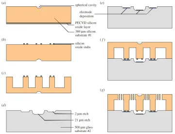
The fabrication process of the three-dimensional actuator is illustrated in figure 10. Starting with the PECVD deposition of a 1µm thick silicon oxide layer on the back of a 380µm silicon substrate (figure 10(a)), the spherical cavity is processed on the front side of the substrate #1. After the silicon oxide layer is masked and dry etched to obtain the silicon oxide stubs, (figure 10(b)) a deep reactive ion etching process is applied etching 320 µm deep into the silicon substrate forming the rigid anchor posts and pillar structures (figure 10(c)).
Next, a 500µm glass substrate (substrate #2) is prepared by wet etching one 21 µm deep cavity and four 2 µm deep cavities (figure 10(d)). On the bottom surface of the cavities the metal electrodes are patterned from a layer of gold evaporated onto the substrate surface (figure 10(e)). Finally both substrates #1 and #2 are anodically bonded (figure 10(f)) and exposed to a second deep dry-etch of 60µm which releases the actuation structure (figure 10(g)).
[image:5.595.296.526.296.473.2](d)
(g)
2 µm etch
21 µm etch
[image:6.595.109.469.70.346.2]500 µm glass substrate #2
Figure 10.Overview of the fabrication process of the three-dimensional actuator.
(a)
(b)
(c)
Figure 11.Overview of the fabrication process of the two-dimensional actuator.
the in-plane actuator that is used solely for the optical cavity alignment is fabricated. A second fabrication process is applied to add the out-of-plane actuation that is used for tuning the optical cavity. Without any actuation in thez direction the full fabrication process can be simplified as shown in figure 11.
On the front of a 380µm thick silicon substrate (substrate #1 in figure 11(a)) a spherical cavity is processed [18]. Then, a deep-dry etch of 320 µm is applied to the back side of this wafer, forming the rigid anchor posts of thexy-actuation structure. After anodically bonding the silicon substrate #1 to the glass substrate #2 (figure 11(b)), a second 60 µm
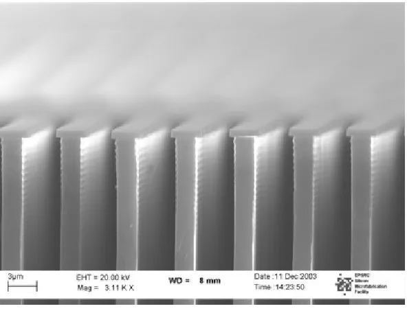
dry-etch from the front is carried out releasing thexy-actuator (figure 11(c)). So far we have processed the xy-actuator. Figure 12 shows SEM images after each processing step. Figure 13 is a SEM image of the finalxy-actuation structure. At the moment thexy-actuation device is being prepared for testing the actual translation that can be achieved. These results can then be compared to our analytical and simulated findings.
[image:6.595.48.279.386.567.2]Since the surface of the 320µm deep dry-etch forms the bottom plane of the comb fingers, it is crucial for the design evaluation that the bottom plane that is a part of the comb drives is smooth. For example, a deformation around the suspension of the rigid anchor posts results in an irregularity of the attached suspension beams which makes the system less controllable and less predictable. In order to rule out any conflict between the design and the fabrication process, the surface roughness in the 320µm etched surface plane was investigated. Figure 14 shows an AFM measurement of the surface, which is then used to determine the roughness of the 320 µm deep surface. The RMS surface roughness was measured to be 26 nm, which is well in agreement with the design objectives.
(a) (b)
[image:7.595.51.530.63.453.2](c) (d)
Figure 12. SEM images of the fabrication results after each processing step: (a) rigid anchor posts formed after the 1st etch, (b) anodic bonding, (c) releasing the structure after the 2nd etch and (d) the comb drive fingers.
Figure 13.SEM image of the finalxy-actuator.
[image:7.595.49.282.497.675.2]specified by the manufacturer of the etching apparatus to be a maximum of 250 nm. The undercut of the 3µm masked resist layer on top of the comb fingers can clearly be seen in figure 15.
Figure 14.AFM measurement on the 320µm etched surface.
[image:7.595.305.513.500.646.2]Figure 15.Broadening of the gap due to undercut during deep dry-etching.
6. Conclusions
A three-dimensional electrostatic actuator that can be integrated on atom chips was presented. The device incorporates a unique locking mechanism securing the xy -actuation stage at a pull-in voltage ofVPI,L=140 V expecting
to enhance the mechanical stability of the optical cavity. The electrostaticxyz-actuator uses several comb drive structures for thexy-actuation allowing a translation of 17.5µm with an accuracy in the sub-micron range and a parallel plate configuration for thez-actuation with a maximum translation of 7µm with an envisaged accuracy of a few nanometers. A design and simulation evaluation was carried out on the three-dimensional actuation device. Both analytical calculations and simulation results of the actuation showed that sufficient translation for alignment and tuning of a microcavity can be achieved. The fabrication process of the device was outlined and preliminary results of the fabrication process of the
xy-actuator were presented.
References
[1] Hinds E A and Hughes I G 1999 Magnetic atom optics: mirrors, guides, traps, and chips for atomsJ. Phys. D: Appl. Phys.32R119–R146
[2] Folman R, Krueger P, Schmiedmayer J, Denschlag J and Henkel C 2002 Microscopic atom opticsAdv. At. Mol. Opt. Phys.48263
[3] Hinds E A, Vale C J and Boshier M G 2001 Two-wire waveguide and interferometer for cold atomsPhys. Rev. Lett.861462
[4] Calarco T, Dorner U, Julienne P S, Williams C J and Zoller P 2004 Quantum computations with atoms in optical lattices: marker qubits and molecular interactionsPhys. Rev.A66
012306
[5] H¨ansel W, Hommelhoff P, H¨ansch T W and Reichel J 2001 Bose–Einstein condensation on a microelectronic chip Nature413498–50
[6] Horak P and Klappauf B G 2003 Possibility of single-atom detection on a chipPhys. Rev.A67043806
[7] Inderm¨uhle P-F, Jaecklin V P, Brugger J, Linder C, De Rooij N F and Binggeli M 1995 AFM imaging with an xy-micropositioner with integrated tipSensors Actuators A46–47562–5
[8] Juan W-H and Pang S W 1998 High-aspect-ratio Si vertical micromirror arrays for optical switching
J. Microelectromech. Syst.7207–13
[9] Akimoto K, Uenishi Y, Honma K and Nagaoka S 1997 Optical reflective filter with comb-drive nickel micromirror for optical fiber communicationElectronic Components and Technologies Conf.pp 614–9
[10] Kim C J, Pisano A P and Mueller R S 1992 Silicon-processed overhanging microgripperJ. Microelectromech. Syst.131–6 [11] Grade J D, Jerman H and Kenny T W 2003 Design of large
deflection electrostatic actuatorsJ. Microelectromech. Syst.
12335–43
[12] Klassen E, Petersen K, Noworolski J M, Logan J, Maluf N I, Brown J, Storment C, McCulley W and Kovacs G 1996 Silicon fusion bonding and deep reactive ion etching: a new technology for microstructuresSensors ActuatorsA52
132–9
[13] Kwon S, Milanovic V and Lee L P 2002 Large-displacement vertical microlens scanner with low driving voltagePhoton. Technol. Lett.141572–4
[14] Rembe C, Muller L, Muller R S and Howe R T 2001 39th Annu. Int. Reliability Physics Symp.pp 91–8 [15] Zhou T, Wright P, Crawford J, McKinnon G and Zhang Y
2003 MEMS 3D optical mirror/scannerInt. Conf. on MEMS, NANO and Smart Systemspp 222–6
[16] Ando Y 2004 Development of three-dimensional electrostatic stages for scanning probe microscopeSensors Actuators A114285–91
[17] Koukharenko Eet al2004 Microfabrication of gold wires for atom guidesSensors ActuatorsA115600–7
[18] Moktadir Z, Koukharenka E, Kraft M, Bagnall D M, Powell H, Jones M and Hinds E A 2004 Etching techniques for realizing optical micro-cavity atom traps on silicon J. Micromech. Microeng.14S82–S85
[19] Tang W C 1990PhD dissertationCalifornia University, CA [20] Nemirosky Y and Bochobza-Degani O 2001 A methodology
and model for the pull-in parametersJ. Microelectromech. Syst.1601–15