DC TO DC CONVERTER USING CMOS
MUHAMMAD ISMINHAZWAN BIN ISMAIL
This report is submitted in partial fulfillment of the requirement for the award of Bachelor of Electronic Engineering (Industrial Electronics) With Honours
Faculty of Electronic and Computer Engineering University Technical Malaysia, Melaka
I'SI\'ERSITI TEIiKIIiAL .\LaLAYSU Y 1 E L . W
FAhl-IT1 U J l r R I T E R 4 A N ELERTROSK DAY KE.n.RYTER4.4S KCb\IPI.TER
BOR,\SC PESCIS,\KLY STATZ'S L\WR\S
PROJEK SARJ.4S.AInD.A 11
..I,
Tajuk Projek : DC to DC Converter Csmg CMOS
me~l&&--~ alzlnbaurkna Lnyora~i Plojek Sa~jaaa 3Iuda illi diiill~yan di Pwusraka~l~ deligal syarnt- syrat keput~aan szycni b e ~ i h a :
1. L a p o m adalall lkzk 11lil1k L:l~~vaiiri Tehlikel Malaysia Sfelaka. 2. Paparakaal~ diba~x-kar~ luaiibt~ar salinal~ ~u~tilk 11!jlla11 p a ~ p i ~ i a l r 5allajn.
3. Pay~ntaknaa dihalarkn~i mcmb~~ar s a l i ~ ~ a n lapaan mi sebgni balls11 p n i k a r a l ~ alltan illstitlrii
~?ensa.iian tinepi.
4 . Sila tandikan ( \ i -
!>ltnpa>duupi nmkl~unt yalg berdmjah hxl.m~~:sn atau
kqm~tmgan Malayis s t p m i !-a$ taulmlmb di dda~l AKT.4
RXlISW PASh,tlI???l
DAXD i . XTIS) (COP DAY TA?JDATkYGGIY PESTELLXI
xlan.lt lcuy. SO. 10 Kg Tanah Sferah, Lubok Kan-ah,
2SOOO Temerloh
"I hereby declare that this report is the result of my own work except for quotes as cited
in the references."
Signature
Author
Date
.F& :far:',,
kulti Kej E:r;.'-nv-i* 92 '.;:.s: <i)m@t,it! 'C-YFKK),
. . .
.
,~l~iypr#i.~qk?i.kai tf?l?.y:la Melaka (UTeM),:
...
b&
Karung berkicnci 120C."I hereby declare that I have read this report and in my own opinion this report is
sufficient in terms of the scope and quality for the award of Bachelor of Electronic
Engineering (Industrial Electronics) With Honours."
Signature
Supervisor's Name
Date
TULKAR#A;w O 2:l;Li;;;rr Pensyilra.1
akuli K r j Ekk'r)nik d a l Kei Kornplrter 'FKEKK),
Special dedicated to my beloved parents, family, lecturers, friends, who had strongly
ACKNOWLEDGEMENT
I have completed my thesis which is a partial fulfilment of requirements for the
degree of Bachelor in Electronic Engineering (Industrial Electronic).
On this opportunity, I would like to express my gratitude to the Faculty of
Electronic Engineering, Universiti Teknikal Malaysia Melaka generally and especially
to my supervisor En Zulkarnain Bin Zainudin for her help, advices and guidance
throughout the process of searching, collecting information, analyzing and completing
the report.
To my parents, I would like to express million of thanks to them for their support
and love to me. Last but not least, I would like to thank to all my friends in 4 BENE and
vii
ABSTRACT
In this DC to DC Converter using CMOS, the theory of this method is to build a
DC to DC converter that can step-up the input voltage to the desired output voltage.
Designing the circuit based on the basic of boost converter circuit that consist of
inductor, diode, dc supply, capacitor and a switching component. From these
components with their characteristic will act to produce the desired output voltage. This
method also has its disadvantage as stated in chapter before. The problem statement is
Conventional dc power supplies are designed to operate at a given output voltage into a
constant or near-constant load. Pulse lasers, flash lamps, rail guns, and other pulse power
systems, however, require short but intense bursts of energy that may be derived from
rapidly charging an energy storage capacitor. Some objectives are to understand and
design a DC to DC converter using CMOS, to generate the desired output voltage, and to
learn well about programming software that will be used. The methodology for this
project is firstly preparing Gantt chart, doing literature review and software simulation
and demonstration of the project. The result hopehlly can fulfill the theory DC to DC
converter using CMOS which the main point is to generate the desired DC output
...
V l l l
ABSTRAK
DC kepada DC Converter menggunakan CMOS, teori kaedah ini adalah membina satu
penukar DC kepada DC yang boleh menaik voltan keluaran yang diingini daripada
voltan masukan. Litar ini adalah berdasarkan tentang litar peningkatan penukar asas
yang mengandungi induktor, diod, dc supply, kapasitor dan sebuah komponen
pensuisan. Daripada komponen-komponen ini dengan ciri mereka, akan bertindak
menghasilkan voltan keluaran yang diinginkan. Kaedah ini juga mempunyai
kekurangan seperti yang akan dinyatakan dalam bab di hadapan. Kenyataan masalah
adalah bekalan tenaga biasa dc adalah direka untuk beroperasi di bagi satu voltan
keluaran ke dalam satu pemalar. Beberapa objektif adalah akan memahami dan reka
bentuk satu DC untuk penukar DC menggunakan CMOS, untuk menjana voltan
keluaran terhasrat, dan mempelajari mengenai perisian pengaturcaraan yang akan
digunakan. Kaedah untuk projek ini adalah mula-mula menyediakan carta Gantt,
melakukan ulasan karya dan perisian simulasi dan dernonstrasi projek ini. Semoga hasil
projek ini boleh memenuhi teori penukar DC kepada DC menggunakan CMOS yang
mana asasnya adalah untuk menjana voltan keluaran DC daripada satu voltan masukan
CONTENTS
CHAPTER TITLE
PROJECT TITLE VERIFICATION FORM DECLARATION VERIFICATION DEDICATION ACKNOWLEDGEMENT ABSTRACT ABSTRAK CONTENTS FIGURES LIST
SYMBOL, SHORT FORM & TERM LIST
INTRODUCTION
1.1 INTRODUCTION OF THE PROJECT
1.2 PROJECT OBJECTIVES
1.3 PROBLEM STATEMENT
1.4 SCOPE OF WORK
1.5 METHODOLOGY
I1 LITERATURE REVIEW
2.1 CMOS
2.2 CAPACITOR
2.2.1 Stored Energy
2.3 DIODE
2.3.1 Semiconductor Diode
2.4 IGBT
2.4.1 Basic Structure and Operation
2.4.2 Static Characteristics
2.4.3 Dynamic Switching Characteristics
2.4.4 IGBT Performance Parameters
2.4.5 Gate Drive Requirements
I11 PROJECT METHODOLOGY
3.1 LITERATURE REVIEW
3.2 DESIGN THE CIRCUIT
3.3 FLOW CHART
RESULT AND ANALYSIS
4.1 RESULT
4.2 TROUBLESHOOTING
5.1 DISCUSSION AND SUGGESTION
5.2 CONCLUSION
REFERENCES
FIGURE LIST
TITLE PAGE
Boost Converter 5
Waveforms 8
Diodes 13
I-V characteristics of a P-N junction diode (not to scale) 15
Hybrid Darlington configuration of MOSFET and BJT 19
The IGBT (a) half-cell vertical cross section and (b) equivalent
circuit model 2 1
The IGBT (a) forward- and (b) transfer characteristics 22
Punch-through (PT) IGBT 23
The IGBT equivalent circuits (a) BJT=MOSFET, and
(b) pin=MOSFET 25
Components of on-state voltage drop within the IGBT structure 27
Trench IGBT structure 28
The IGBT turn-on waveforms in a clamped inductive load circuit 29
Switching waveforms during IGBT clamped inductive load turn-off 31
On-state current flow paths in an IGBT structure 34
The IGBT safe operating area (SOA) 3 9
Gate-drive circuit with independent turn-on and turn-off resistors 41
External gate capacitor for decoupling dv,Jdt and di,=dt
during switching transient 41
A circuit for reducing the turn-on delay 43
Schematic circuit of an IGBT gate-drive circuit 43
4.1 Desired Output Voltage 5 2
4.2 Maximum Output Voltage 5 3
5.1 Three modes of operation of a capacitor charging power supply 5 7
5.2 Power requirements for pulsed power and constant power loads 58
SYMBOL, SHORT FORM & TERM LIST DC CMOS CCPS LED IGBT MOSFET FBSOA SOA BVCES BVECS VGES Ic ICM PD
Tj
ILM ICESV G E ( ~ ~ )
VCE(SAT)
~ F E
QG
t d
t ,
Direct Current
Completmentary Metal-Oxide-Semiconductor
Capacitor charging power supply
Light-emitting diode
Insulated gate bipolar transistor
Metal oxide field effect transistors
Forward-biased safe operating area
Safe operating area
Collector-Emitter Blocking Voltage
Emitter-Collector Blocking Voltage
Gate-Emitter Voltage
Continuous Collector Current
Peak Collector Repetitive Current ICM
Maximum Power Dissipation
Junction Temperature
Clamped Inductive Load Current
Collector-Emitter Leakage Current
Gate-Emitter Threshold Voltage
Collector-Emitter Saturation Voltage
Forward Transconductance
Total Gate Charge
Turn-on Delay Time
h o r n Turn-off Delay Time
t f Fall Time
Cies Input Capacitance
CO, Output Capacitance
CHAPTER 1
INTRODUCTION
1.1 Introduction to project
This paper concerns the design and implementation of a DC-DC Converter using
CMOS. This design is based on a basic boost converter with a little adjustment. It can be
used for many applications but is best for charging capacitor banks. The input voltage
will be 12V DC, 12V is used for many applications and it is easy to get battery or dc
input voltage that supply 12V. The output voltage will be around 280V to 600V. The
operation of this DC to DC converter is applied from a basic boost converter. Boost
converter is a dc-to-dc converter that steps up the dc voltage from its fixed low level to a
desired high level. It is also called the fly-back converter because the energy transfer,
from the source to the load, takes place only during the off period of the switch. The
high output voltage is suitable for many applications that require high-quality, small,
1.2 Project Objectives
The objectives for this project are:
1. To understand and design a DC-DC converter using CMOS
2. To generate the desired high DC output voltage
3. To learn and understand very well how to use programming software.
For the first objective, for this project I have to understand very well the whole thing
about my final my project that is a DC-DC converter using CMOS. After understanding
the project very well, I will be able to design this converter.
After finishing designing and completing the prototype of the circuit, I must be able to
generate the desired high DC output voltage that vary from 280V to 600V. In order to
achieve that, I must understand very well the basic design of boost converter and the
operation of the entire component that I have chosen for this DC-DC converter.
I must also learn and understand very well how to use programming software. In this
project, I will be using PSPICE, MULTISIM, and PROTEUS. These programming
software will be used to generate and simulate the desired circuit that will be used in this
1.3 Problem Statement
Modem electronic systems require high-quality, small, lightweight, reliable, and
efficient power supplies. Linear power regulators, whose principle of operation is based
on a voltage or current divider, are inefficient. This is because they are limited to output
voltages smaller than the input voltage, and also their power density is low because they
require low frequency (50 or 60 Hz) line transformers and filters. Linear regulators can,
however, provide a very high-quality output voltage. Their main area of application is at
low power levels. Electronic devices in linear regulators operate in their active (linear)
modes, but at higher power levels switching regulators are used. Switching regulators
use power electronic semiconductor switches in on and off states. Because there is a
small power loss in those states (low voltage across a switch in the on state, zero current
through a switch in the off state), switching regulators can achieve high energy
conversion efficiencies. Modem power electronic switches can operate at high
frequencies. The higher the operating frequency, the smaller and lighter the
transformers, filter inductors, and capacitors. In addition, the dynamic characteristics of
converters improve with increasing operating frequencies. The bandwidth of a control
loop is usually determined by the comer frequency of the output filter. Therefore, high
operating frequencies allow for achieving a faster dynamic response to rapid changes in
the load current andfor the input voltage. Conventional dc power supplies are designed
to operate at a given output voltage into a constant or near-constant load. Pulse lasers,
flash lamps, rail guns, and other pulse power systems, however, require short but intense
bursts of energy that may be derived from rapidly charging an energy storage capacitor.
The rate at which the capacitor discharges is called the repetition rate and may vary from
0.01 Hz for large capacitor banks to a few kilohertz for certain lasers. After the energy
storage capacitor is discharged, it must be recharged to a specified voltage using a
1.4 Scope of Work
1) Analyze and research the design of a DC-DC converter using CMOS:
a. Study and research of design of the DC-DC converter using CMOS.
b. Study and research of operation of a basic boost converter.
c. Study and research the components that are going to be used for the
design.
d. Obtaining the result of simulation.
2) Design the circuit of a DC-DC converter using CMOS:
a. Identify the suitable components for the designed circuit.
b. Simulate the designed circuit.
c. Study the result of the simulated circuit.
3) Construct the designed circuit
a. Construct the designed circuit based on programming sofhare.
b. Study the appropriate component to be used for constructing the designed
circuit.
c. Test and compare the determined result to expected result.
4) Build the prototype of the circuit
a. Design the casing for the prototype
1.5 Methodology
Boost Converter
Boost converter is a dc-to-dc converter that steps up the dc voltage from its fixed low
level to a desired high level. It is also called the fly-back converter because the energy
transfer, from the source to the load, takes place only during the off period of the switch.
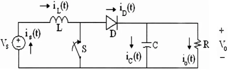
[image:20.542.82.473.259.386.2]Its circuit topology is given in Figure 1.
Figure 1.1: Boost Converter
The switch S is usually an electronic device that operates either in the conduction mode
(on) or the cut-off mode (off). The on and off time-periods are controlled by the suitably
designed gating circuits, which are usually not shown. The on time of the switch is a
fraction of its time period T such that ToN=DT, where D is the duty cycle.
During the on time the inductor current increases from its minimum value toward its
maximum value. In other words, the stored energy in the inductor increases during the
time the switch is in the closed position. During the off time, TOFF= (1-D)T, the switch is
open and the inductor current is directed toward the load via diode D. The inductor
current therefore charges the capacitor and supplies the load current. The diode D blocks
not only the current flow toward the -source when the switch is in the closed position but
also stops the output voltage from appearing across the closed switch. The inductor also
operating in the continuous conduction mode. The capacitor C provides the filtering
action by providing a path for the harmonic currents away from the load. In addition, its
value is large enough so that the output voltage ripple is very small.
Using Faraday's law for the boost inductor
VsDT = (Vo-Vs)(l -D)T
From which the dc voltage transfer fbnction turns out to be
M V VoNs = Ill-D
As the name of the converter suggests, the output voltage is always greater than the
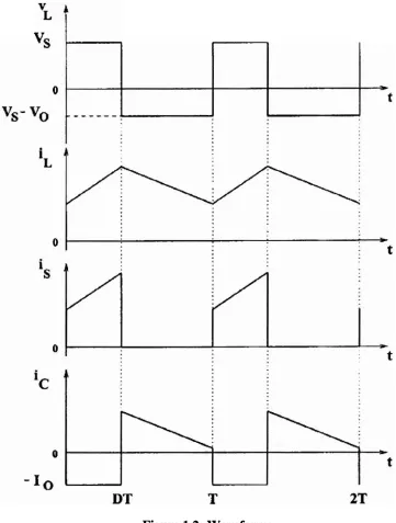
Figure 1.2: Waveforms
As shown in Fig. 2.2, the current supplied to the output RC circuit is discontinuous.
Thus, a larger filter capacitor is required in comparison to that in the buck-derived
converters to limit the output voltage ripple. The filter capacitor must provide the output
dc current to the load when the diode D is off. The minimum value of the filter
CHAPTER 2
LITERATURE REVIEW
2.1 Completmentary Metal-Oxide-Semiconductor (CMOS)
Complementary metal-oxide-semiconductor (CMOS) is a major class of integrated
circuits. CMOS technology is used in microprocessors, microcontrollers, static RAM,
and other digital logic circuits. CMOS technology is also used for a wide variety of
analog circuits such as image sensors, data converters, and highly integrated transceivers
for many types of communication.
CMOS is also sometimes referred to as complementary-symmetry metal-oxide-
semiconductor. The words "complementary-symmetry" refer to the fact that the typical
digital design style with CMOS uses complementary and symmetrical pairs of p-type
and n-type metal oxide semiconductor field effect transistors (MOSFETs) for logic
functions.
Two important characteristics of CMOS devices are high noise immunity and low static
power consumption. Significant power is only drawn when the transistors in the CMOS
device are switching between on and off states. Consequently, CMOS devices do not
produce as much waste heat as other forms of logic, for example transistor-transistor
The phrase "metal-oxide-semiconductor" is a reference to the physical structure of
certain field-effect transistors, having a metal gate electrode placed on top of an oxide
insulator, which in turn is on top of a semiconductor material. Instead of metal, current
gate electrodes (including those up to the 65 nanometer technology node) are almost
always made from a different material, polysilicon, but the terms MOS and CMOS
nevertheless continue to be used for the modern descendants of the original process.
Metal gates have made a comeback with the advent of high-k dielectric materials in the
CMOS process, as announced by IBM and Intel for the 45 nanometer node and beyond.
CMOS logic uses a combination of p-type and n-type metal-oxide-semiconductor field-
effect transistors (MOSFETs) to implement logic gates and other digital circuits found in
computers, telecommunications equipment, and signal processing equipment. Although
CMOS logic can be implemented with discrete devices (for instance, in an introductory
circuits class), typical commercial CMOS products are integrated circuits composed of
millions (or hundreds of millions) of transistors of both types on a rectangular piece of
silicon of between 0.1 and 4 square centimeters. These devices are commonly called
"chips", although within the industry they are also referred to as "die" (singular) or
"dice" (plural).
In CMOS logic, a collection of n-type MOSFETs are arranged in a pull-down network
between the output node and the lower-voltage power supply rail, named V,,, which
often has ground potential. Instead of the load resistor of NMOS logic gates, CMOS
logic gates have a collection of p-type MOSFETs in a pull-up network between the
output and the higher-voltage rail, named Vdd. Pull-up and pull-down refer to the idea
that the output node, which exhibits some internal capacitance, is charged or discharged
by the connected pull-up and pull-down networks. By asserting or de-asserting the
inputs to the CMOS circuit, individual transistors along the pull-up and pull-down