Rochester Institute of Technology
RIT Scholar Works
Theses Thesis/Dissertation Collections
6-20-2014
Material Engineering for Phase Change Memory
David Cabrera
Follow this and additional works at:http://scholarworks.rit.edu/theses
This Thesis is brought to you for free and open access by the Thesis/Dissertation Collections at RIT Scholar Works. It has been accepted for inclusion in Theses by an authorized administrator of RIT Scholar Works. For more information, please [email protected].
Recommended Citation
R
·
I
·
T
Material Engineering for Phase Change Memory
by
David Cabrera
A Thesis Submitted in Partial Fulfillment of the
Requirements for the Degree of Master of Science
In Electrical and Microelectronic Engineering
Department of Electrical and Microelectronic Engineering
Kate Gleason College of Engineering
Rochester Institute of Technology
Rochester, NY
i
Material Engineering for Phase Change Memory
By
David M. Cabrera
A Thesis Submitted
In Partial Fulfillment
Of the Requirements for the Degree of
Master of Science
In
Electrical and Microelectronic Engineering
Approved By:
Prof. ________________________________
Dr. Santosh K. Kurinec (Thesis Advisor)
Prof. ________________________________
Dr. Robert E. Pearson
Prof. ________________________________
Dr. Ivan Puchades
DEPARTMENT OF ELECTRICAL AND MICROELECTRONIC ENGINEERING
COLLEGE OF ENGINEERING
ii
Material Engineering for Phase Change Memory
By
David M. Cabrera
I, David M. Cabrera, hereby grant permission to the Wallace Memorial Library of the Rochester Institute of Technology to reproduce this document in whole or in part and that any reproduction will not be for commercial use or profit.
________________________________ ____________________
iii
Acknowledgements
I’d like to thank the following people for all their help and support:
My family
The Microelectronic Engineering Faculty which includes My thesis committee
Dr Santosh Kurinec Dr Robert Pearson Dr Ivan Puchades
All of the SMFL staff
Dr Simone Raoux from IBM TJ Watson Research Center
iv
Abstract
As semiconductor devices continue to scale downward, and portable consumer electronics become more prevalent there is a need to develop memory technology that will scale with devices and use less energy, while maintaining performance. One of the leading prototypical memories that is being investigated is phase change memory. Phase change memory (PCM) is a non-volatile memory composed of 1 transistor and 1 resistor. The resistive structure includes a memory material alloy which can change between amorphous and crystalline states repeatedly using current/voltage pulses of different lengths and magnitudes. The most widely studied PCM materials are chalcogenides - Germanium-Antimony-Tellerium (GST) with Ge2Sb2Te3 and Germanium-Tellerium (GeTe)
being some of the most popular stochiometries. As these cells are scaled downward, the current/voltage needed to switch these materials becomes comparable to the voltage needed to sense the cell’s state. The International Roadmap for Semiconductors aims to raise the threshold field of these devices from 66.6 V/μm to be at least 375 V/μm for the year 2024. These cells are also prone to resistance drift between states, leading to bit corruption and memory loss.
Phase change material properties are known to influence PCM device performance such as crystallization temperature having an effect on data retention and litetime, while resistivity valuesin the amorphous and crystalline phases have an effect on the current/voltage needed to write/erase the cell. Addition of dopants is also known to modify the phase change material parameters.
The materials G2S2T5, GeTe, with dopants - nitrogen, silicon, titanium, and aluminum oxide and undoped
Gallium-Antimonide (GaSb) are studied for these desired characteristics. Thin films of these compositions are deposited via physical vapor deposition at IBM Watson Research Center. Crystallization temperatures are investigated using time resolved x-ray diffraction at Brookhaven National Laboratory. Subsequently, these are incorporated into PCM cells with structure designed as shown in Fig.1. A photolithographic lift-off process is developed to realize these devices. Electrical parameters such as the voltage needed to switch the device between memory states, the difference in resistance between these memory states, and the amount of time to switch are studied using HP4145 equipped with a pulsed generator.The results show that incorporating aluminum oxide dopant into G2S2T5 raises its threshold field from 60 V/μm to 96 V/μm, while for GeTe, nitrogen doping raises its threshold
field from 143 V/μm to 248 V/μm. It is foundthat GaSb at comparable volume devices has a threshold field of 130 V/μm. It was also observedthat nitrogen and silicon doping made G2S2T5 more resistant to drift, raising time to drift
from 2 to 16.6 minutes while titanium and aluminum oxide doping made GeTe drift time rise from 3 to 20 minutes. It was also foundthat shrinking the cell area in GaSb from 1 μm2 to 0.5 μm2 lengthened drift time from 45s to over 24 hours.
The PCM process developed in this study is extended to GeTe/Sb2Te3multilayers called the superlattice
(SL) structure that opens opportunities for future work. Recent studies have shown that the superlattice structure exhibits low switching energies, therefore has potential for low power operation.
v
Table of Contents
Chapter 1 – Introduction... 1
1.1– Overview of Semiconductor Memory Technology ... 1
1.2– DRAM Memory ... 4
1.3– Flash Memory ... 5
Chapter 2 – Background of Phase Change Memory ... 9
2.1 – Phase Change Memory Background ... 9
2.2 – Phase Change ... 10
2.3 – Current Technology Phase Change Memory ... 13
2.4 – Future Phase Change Memory Trends ... 14
Chapter 3 – Thesis Objectives ... 17
3.1 – Motivation ... 17
Chapter 4 – Fabrication ... 18
4.1 – Introduction ... 18
4.2 – Mask Set Design... 19
4.3 – Process Flow for Device Fabrication ... 20
Chapter 5 – PCM Cells with Droped GST & GeTe ... 27
5.1 – Dopant Effects in Phase Change Memory Introduction ... 27
5.2 – Device Fabrication ... 28
5.3 – Time-Resolved XRD Analysis ... 29
5.4 – Structural Results ... 30
5.5 – Electrical Results ... 33
5.6 – Conclusions ... 35
Chapter 6 – Investigating Resistance Drift ... 37
6.1 – Introduction to Resistance Drift ... 37
6.2 – Resistance Drift ... 38
6.3 – Drift Measurements ... 39
vi
Chapter 7 – Gallium Antimonide PCM... 41
7.1 – GaSb Introduction ... 41
7.2 – Device Creation ... 42
7.3 – Electrical Results ... 43
7.4 – Drift Measurements ... 45
7.5 – Conclusions ... 46
Chapter 8 – Superlattice PCM ... 48
8.1 – Superlattice Introduction ... 48
8.2 – Superlattice ... 48
8.3 – Device Creation ... 50
8.4 – Electrical Results ... 52
8.5 – Drift Measurements ... 52
8.6 – Conclusions ... 53
Chapter 9 – Conclusions and Future Work ... 54
vii
List of Tables
Table 5.1 - Phase Change Material Parameters and the Influenced Characteristics ... 27
Table 5.2 - Summary of Doped PCM Film Compositions ... 28
Table 5.3 - Summary of Threshold Field and ON/OFF Ratio in Doped Devices ... 35
Table 6.1 - Summary of Drift Time for Doped PCM Devices ... 40
Table 7.1 - Summary of Findings for GaSb Devices of Different Dimensions ... 45
Table 7.2 - Summary of Drift Time for GaSb Devices of Different Dimensions... 45
Table 7.3 - Summary of Drift Time for GaSb Devices for Different Pulse Characteristics ... 46
viii
List of Figures
Figure 1.1 Memory hierarchy by type (on right), with includes volatility and retention length
inside the triangles, and examples on left. ... 2
Figure 1.2 Memory hierarchy divided by volatility. ... 3
Figure 1.3 Typical memory components in a computer, structured by access latency. Types of memory are encircled. ... 4
Figure 1.4 DRAM memory configuration. ... 5
Figure 1.5 Cross section of a typical flash memory structure. ... 6
Figure 1.6 NOR flash memory configuration. ... 6
Figure 1.7 NAND flash memory configuration. ... 7
Figure 1.8 Phase change memory structure. ... 8
Figure 2.1 Ternary phase diagram depicting chalcogenide alloys, with year of discovery and their uses. [6] ... 10
Figure 2.2 I-V characteristics of a phase change memory device showing switching between resistive states. ... 11
Figure 2.3 Phase change memory pulse time vs. temperature to reach different states. ... 12
Figure 2.4 Umbrella flip model during switching of GST, between a tetrahedral (left) and octahedral (right) configuration [8]. ... 13
Figure 2.5 Potential of phase change memory compared to industry standard, adapted from ITRS ... 14
Figure 2.6 PCM Technological requirements. Yellow cells have manufacturable solutions, while red cells do not. (ITRS)... 15
Figure 4.1 Cross sectional view of memory cell design. ... 17
Figure 4.2 (a) Sample test structure for (b) mask designed for Canon lithography tool. ... 18
Figure 4.3 (a) Sample test structure for (b) mask designed for ASML lithography tool. ... 19
Figure 4.4 Process flow chart divided by lithography step. ... 20
Figure 4.5 Atomic force microscopy of a cell after lift-off process. ... 23
ix
Figure 4.7 PCM devices, active area located within the delineated circle.. ... 25
Figure 5.1 Time resolved XRD measurements on GST and GeTe, centered on 2θ = 31ᵒ. ... 28
Figure 5.2 Time resolved XRD measurements on different dopant compositions plot as the intensity of the peaks vs. temperature as was ramped. These show the transition between amorphous and crystalline states for the materials investigated. ... 30
Figure 5.3 θ-2θ scans of undoped and doped, GST and GeTe respectively, after a ramp to 450ᵒC. . ... 31
Figure 5.4 Resistivity as a function of temperature for undoped and doped, GST and GeTe respectively. ... 32
Figure 5.5 Representative electrical data for doped and undoped GST. ... 33
Figure 5.6 Representative electrical data for doped and undoped GeTe. ... 33
Figure 5.7 Graphical representation of threshold field vs. dopant compositions investigated. ... 35
Figure 6.1 Chalcogenide material drift from amorphous to crystalline state. ... 37
Figure 6.2 Chalcogenide material drift from crystalline to amorphous state. ... 37
Figure 6.3 Resistance Drift in doped GST devices. ... 38
Figure 6.4 Resistance Drift in doped GeTe devices... 39
Figure 7.1 Ternary phase diagram depicting different GaSbTe compositions and their respective crystallization temperature. [28] ... 41
Figure 7.1 Representative electrical data for 0.5 μm sized devices. ... 42
Figure 7.2 Representative electrical data for 1.0 μm sized devices. ... 43
Figure 7.3 Summary of threshold field in GaSb cell dimensions. ... 46
Figure 8.1 (a) Ge is in a tetrahedral environment in amorphous GST and transitions to octahedral in its cubic crystalline phase; (b) Crystal schematic of GeTe/Sb2Te3 superlattice; (c) Superimposed images of two projected sheets of GeTe/Sb2Te3. Ge atoms (with arrows) in GeTe layers move forwards and backwards to the interface with Sb2Te3 layers. ... 48
Figure 8.2 EELS line scan showing superlattice layers present in device. ... 49
Figure 8.3 TEM showing superlattice layers present in device (darkest layer)... 50
x
List of Symbols
xi
List of Acronyms
RIT Rochester Institute of Technology
VLSI Very Large Scale Integrated
RAM Random Access Memory
DRAM Dynamic RAM
SRAM Static RAM
ROM Read Only Memory
NVROM Non-Volatile ROM
PROM Programmable Read-Only Memory
STT-MRAM Spin Tranfer Torque Magnetoresistive RAM
FeRAM Ferroelectric RAM
PCM Phase Change Memory
SD Secure Digital
ITRS International Technology Roadmap for Semiconductors
PECVD Plasma-Enhanced Chemical Vapor Deposition
EDAX Energy-Dispersive X-ray Spectroscopy
GST Germanium Antimony Telluride
GeTe Germanium Telluride
XRD X-ray Diffraction
GaSb Gallium Antimonide
1
Chapter 1
Introduction
Semiconductor memories are an important part of modern day technology, and like all
modern technology, it needs to grow in performance and density to keep furthering technological
advancement. This advancement has driven rapid growth of very large scale integrated (VLSI)
systems for a wide range of applications, including personal and commercial computing,
consumer electronics, smart phones, tablets, sensors for different applications, and even medical
devices. To keep up with demand for high performance, low-power applications, it is required to
have a large amount of low-power embedded memory to support the data bandwidth needed for
high performance computing. Typical semiconductor memory is an electronic device used to
store data, implemented on a semiconductor circuit.
1.1 Overview of Semiconductor Memory Technologies
Memory is often divided into primary storage, secondary storage, and tertiary storage
which takes in consideration the speed and cost of the component, as seen in figure 1.1. Primary
storage is what is most commonly referred to as internal memory. This category is composed of
the fastest components, which also tend to be the costliest. Unfortunately, this type of memory
loses data when it is powered down. This type of memory includes processor registers, processor
cache, and main memory. Secondary storage is usually known as external memory. This type of
memory has an average speed for an average cost, but it does not lose data when powered down.
This type of memory includes memory sticks, hard drives, CD/DVD and solid state drives.
Tertiary storage is the slowest level of storage, which is often used for archiving information
2
Figure 1.1 Memory hierarchy by type (on right), with includes volatility and retention length inside the triangles, and examples on left.
Memory can be further divided within two types, volatile and non-volatile memory, as
seen in figure 1.2. Volatile memory requires power to maintain storage, while non-volatile does
not. Current volatile memories being used today include all types of primary memory such as
Random Access Memory (RAM) which includes Dynamic RAM (DRAM) and Static RAM
(SRAM). These memories have been utilized as primary cache memories for many electronics
due to their fast read and write performance. Unfortunately, they cannot be used as a storage
3
Figure 1.2 Memory hierarchy divided by volatility.
Non-volatile memories include secondary and tertiary storage such as Read Only
Memory (ROM) and Non-Volatile Read-Only Memory (NVROM) which include various types
of Programmable Read-Only Memory (PROM) and Flash memory. Non-volatile memory is the
type of memory used in storage devices, which include solid state drives, memory cards, USB
drives, etc. These memories are not as fast in terms of read/write performance, but the data is
retained when power is disconnected.
Main memory is the type of memory that has been the focus on development, a primary
storage option with high speed and non-volatility. This emerging technology needs to have
performance that matches DRAM with the capacity and cost of flash memory. These attributes
describe what is often called universal memory. Some of the potential candidates for this
universal memory include spin transfer torque magnetoresistive RAM (STT-MRAM),
ferroelectric RAM (FeRAM), and phase change memory (PCM). The goal of this development is
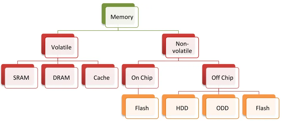
Memory
Volatile
SRAM DRAM Cache
Non-volatile
On Chip
Flash
Off Chip
4
to create compact, robust memory systems with an improved cost to performance ratio relative to
current technology. The defining qualities for this technology include nonvolatility, solid-state
implementation, very low latency, or how fast it takes to receive a data request, (tens to low
hundred nanoseconds), low cost per bit, and physical durability. Figure 1.3 shows typical access
latency (in cycles) of different memory technologies, with their relative place in the memory
hierarchy. Hard disk drive latency is typically four to five orders of magnitude higher than
DRAM. [1] Universal memory should bridge the gap between DRAM and hard disk drives.
Figure 1.3 Typical memory components in a computer, structured by access latency. Types of memory are encircled.
1.2 DRAM Memory
Dynamic random-access memory (DRAM) is the volatile memory industry standard.
Universal memory must be competitive and provide comparable or favorable cost and
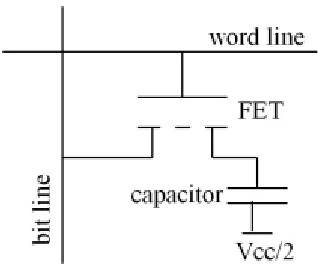
characteristics compared to DRAM. This type of memory is a 1 transistor, 1 capacitor device,
shown in figure 1.4. It was created by Dr. Robert Dennard from IBM and granted a patent in
1968 (U.S. parent number 3,387,286). DRAM is arranged in a matrix with the gates tied together
with a word line, with each transistor having a capacitor on one end, connected to ground, and
5
Figure 1.4 DRAM memory configuration.
Writing to memory consists of biasing the desired word line and bit line to allow the
capacitor to charge or discharge. To read the memory, the bit line is charged up, followed by the
word line connected to a high voltage. This will turn on the selected transistor, and the capacitor
and bit line will share charges. Depending on the voltage the capacitor was holding, the bit line
will have a difference in voltage, which can then be read by a sense amplifier. After each read
operation, the charge on the capacitor is disturbed, so the data needs to be written back to it
(charged or discharged). This type of memory is what is referred to as RAM in modern day
electronic systems.
1.3 Flash Memory
Flash memory is the currently leading industry standard for non-volatile storage devices.
Due to the popularity of flash memory, universal memory needs to be at least as cost effective
and with characteristics that surpass this industry standard. Flash was first invented by Dr. Fujio
Masuoka while working for Toshiba around 1980. [2] Intel introduced the first commercial NOR
flash memory chip in 1988. [3] Flash memory is composed of 1 transistor with two stacked
6
transistor depends on whether the floating gate is charged or not. These transistors are then
arranged in either a NOR or a NAND configuration to create the memory device.
Figure 1.5 Cross section of a typical flash memory structure.
A NOR flash memory configuration can be seen in figure 1.6. The gate is connected to a
word line, while the drain and source are connected to a bit line and to ground. When a positive
bias is applied to the control gate, the channel turns on and the electrons can flow. This current
across the channel causes electrons to move into the floating gate through hot-carrier injection,
programming the cell. Erasing the cell is done by applying an opposite polarity bias to the
control gate, removing the electrons off the floating gate through quantum tunneling. Reading is
done by selecting the appropriate word and bit line.
7
NAND flash memory connects the transistors that compose the memory device in series,
as seen in figure 1.7. These blocks of memory are further linked together in a NOR style
configuration explained previously. Write and erase procedures are done in the same style as the
NOR configuration, although in this configuration, erasing clears whole “blocks” of data due to
the serialized nature.
Figure 1.7 NAND flash memory configuration.
NAND flash is the most common type of flash memory and can be found in many forms,
including USB memory sticks, camera memory storage in the form of compact flash or secure
digital (SD) memory, embedded into MP3 players, game consoles, mobile phones, and even as
the primary storage in solid state drives. The typical size of a flash memory device is about the
size of a postage stamp. Storage capacity is usually anywhere from 512 MB up to 256 GB. This
configuration is economical with a fast read (about 20 MB/s) and a fast write (about 6 MB/s) and
an average erase time (2 ms). NOR based flash memory is costlier and usually used to replace
ROM applications. These have much faster read performance (103 MB/s) but suffer in write
speeds (0.5 Mb/s) and erase speeds (900 ms).
These two types of memories, flash and DRAM, each have the qualities that a universal
8
cost and power, high endurance and scalability, multiple bits per cell, and long retention times.
Phase change memory is a leading prototypical memory technology that can meet all these
standards. Phase change memory (PCM) is a non-volatile memory composed of 1 transistor and
1 resistor. The resistive structure includes a memory material alloy sandwiched between
electrodes, as seen in figure 1.8. These memory materials are composed of elements that belong
to group VIA of the periodic table. These elements are referred to as chalcogens and can form
compounds called chalcogenides. These chalcogenide alloys exist at room temperature in a
stable crystalline phase, and a metastable amorphous phase, with some alloys having additional
metastable phases in between. This material can be switched repeatedly between these two
phases, which have distinct optical and electrical properties.
9
Chapter 2
Background of Phase Change Memory
This chapter provides an overview of phase change materials, including operations and
phenomena that are fundamental to the operation of phase change memory. It concludes with the
current state of phase change technology.
2.1 Phase Change Memory Background
This phase change effect being used as storage was first described [4] and patented [5] by
Stanford Ovshinsky in the 1960s. The lack of fast switching materials prevented development at
that time. In 1987, a new alloy was discovered [6], Ge2Sb2Te3 which led to development of
rewriteable storage technology such as CDs (CD-RW), DVDs (DVD±RW), and most currently
rewritable Blu-ray disks (BD-RE) [7]. The most widely studied PCM materials are alloys of
Germanium-Antimony-Tellerium (GST), seen in figure 2.1, with Ge2Sb2Te3 and GeTe being
10
Figure 2.1 Ternary phase diagram depicting chalcogenide alloys, with year of discovery and their uses. [6]
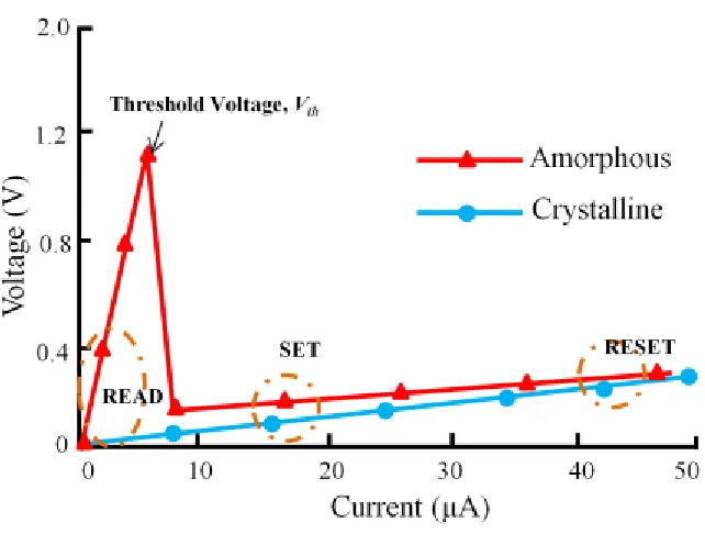
2.2 Phase Change
In its crystalline state, a typical cell reveals ohmic I-V characteristics. When the bias on
the cell is increased, the temperature rises, which causes the GST material to melt. If the current
pulse is quickly dropped off, the molten material has no time to rearrange its bonds and is left in
an amorphous state. In the amorphous state, at low bias, the resistance is very high, which is
termed as the RESET state of the device. Increasing bias in this state will reach a threshold
voltage Vth in which a current path in the amorphous material switches to a highly conductive
11
Figure 2.2 I-V characteristics of a phase change memory device showing switching between resistive states.
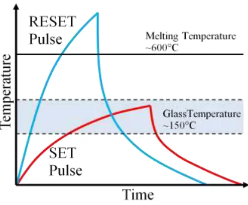
To transition back to a fully crystalline state, a similar current is applied as previously
done, but using lower amplitude and a longer falling edge. This will heat the material into its
glass transition temperature, and give the bonds time to rearrange to the crystalline, low
resistance state, which can be seen in figure 2.3. This low resistance state is termed as the SET
state of the device. The overlap of curves seen on the graph indicates that the device can be
rewritten without an intermediate erase step, a desirable characteristic that simplifies writing to
memory and improves write performance.
The resistivity of the two phases differs by orders of magnitude. Depending on the
material used for the phase change cell, the resistance can vary from a few k in the low
12
Figure 2.3 Phase change memory pulse time vs. temperature to reach different states.
In order to read the memory bit, a very low voltage can be applied, which will cause no
joule heating, thus it will not disturb the cell. In its low resistance state, the voltage applied
across the cell will generate a small amount of current, while in the high resistance state, the
resulting current is practically null. The magnitude of this current can be sensed to evaluate
which logic the cell is at. The difference between the resistances found in the SET and RESET
state can be a few orders of magnitude, this is called the ON/OFF ratio.
Fundamental understanding of the switching process is still being investigated. As GST is
the most widely studied material, it has been found that the Ge atom chances sites during its
atomic configuration. This is called the umbrella flip model, which proposes that the Ge atom
changes from a tetragonally coordinated position in the amorphous phase, to an octahedrally
coordinated site in the crystalline phase [8]. This can be seen in figure 2.4. This could be
13
but the real situation is not as straightforward due to amorphous states lacking long-range
periodicity.
Figure 2.4 Umbrella flip model during switching of GST, between a tetrahedral (left) and octahedral (right) configuration [8].
2.3 Current Technology Phase Change Memory
PMC has been used in test markets inside a Samsung cell phone in 2011 [9]. Since then,
there have been various milestones, including a 20 nm, 8 Gb, 1.8V, 40 MB/s bandwidth PRAM
developed by Samsung in early 2012 [10]. Micron has even started volume production in July
2012 to deliver 45 nm, 1 Gb, low power PCM targeted towards mobile devices [11].
These cells have already shown fast read times (12ns) [12], fast write/erase times (500ps)
[13], low power (100-15 J/bit) [14], low cost (already used in CDs and DVDs) [7], high
endurance (108-1012 cycles) [15], high scalability (3 nm stable films) [16], multiple bits per cell
[17] and long retention time (>10 years) [18]. This displays all the qualities of a universal
14
2.4 Future Phase Change Memory Trends
Currently the International Technology Roadmap for Semiconductors (ITRS) classifies
phase change memory as a prototypical memory, with a very good potential for storage class
applications. This means that it matches or exceeds flash memory for: scalability, multilevel cell
[image:27.612.74.542.234.645.2]storage, 3D integration, low fabrication cost, endurance, and retention. Specifics can be seen in
figure 2.5.
15
Even though it’s predicted that PCM will be extremely viable, there are still some
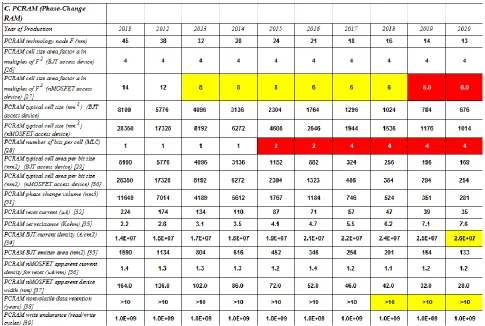
[image:28.612.71.556.163.489.2]challenges to overcome. The technological requirements for PCM to be viable are shown in
figure 2.6.
Figure 2.6 PCM Technological requirements. Yellow cells have manufacturable solutions, while red cells do not. (ITRS)
As can be noted, solutions for device scaling, as well as consistent multi-level cell
16
Chapter 3
Thesis Objectives
This chapter presents the motivation of this investigation, including the goals of this
research.
3.1 Motivation
As cells are scaled downward, Vth will become comparable to the reading voltage needed
to sense the cell’s state. The ITRS predicts that for PCM to be viable, there needs to be a way to
raise the threshold field from the current 66.6 V/μm up to at least 375 V/μm for the year 2024.
This investigation proposes to find new materials with increased threshold field, which is the
ratio of the size and thickness of the cell. Dopants introduced into memory materials could have
an effect on the characteristics of these. A larger difference between resistance in amorphous vs.
crystalline would be very beneficial, further advancing multi-bit densities inside one cell. ITRS
also predicts the need for 4 bits per cell. This ON/OFF ratio will be investigated in all materials
studied. These multi-bit storage options need to be drift resistant. Resistance drift happens when
the cell is not fully amorphized or crystallized, so it will tend to drift towards the prevailing state.
Materials with reduced resistance drift are required as to not lose the stored memory in these
cells. Drift will also be investigated for all the devices created, and attempted to be reduced and
explained. Many applications are also temperature sensitive, such as the automotive industry
which needs devices that can withstand higher temperatures. This investigation will also look
into gallium antimonide, GaSb, a material with high temperature resistance. Lower switching
energies can be beneficial for device scaling. A new device structure, the superlattice, will be
17
Chapter 4
Fabrication
This chapter presents the process from bare wafer to completed device for the phase
change memory cells created.
4.1 Introduction
In this investigation, it was important to create a simple phase change memory cell using
a simple fabrication process with minimal steps. A cross section of the design can be seen in
figure 4.1. The phase change material is sandwiched between a tantalum bottom electrode and an
aluminum top electrode.
Figure 4.1 Cross sectional view of memory cell design.
Tantalum is frequently seen in PCM cell operations, and its ability to withstand high
18
electrode as the heating element to switch the phase of the memory material being used. The
simple design will reduce any fabrication difficulties.
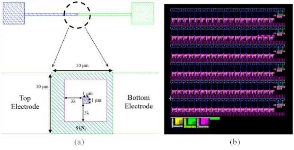
4.2 Mask Set Design
Two different mask sets were used due to an upgrade in lithography tool between
investigations. Both mask layouts were created using the IC Station layout editor from Mentor
Graphics. The first mask set features two terminal PCM cells of varying feature sizes starting
from 1 μm2
and larger, shown in figure 4.2.
Figure 4.2 (a) Sample test structure for (b) mask designed for Canon lithography tool.
This mask layout also included various test structures for evaluating different steps of the
process. This was the first mask set developed for this purpose so test structures were needed for
[image:31.612.76.541.327.561.2]19
The second mask set features two terminal PCM cells of sizes 0.35, 0.4, 0.5 and 1 μm2
with CBKR test structures for measuring contact resistances, shown in figure 4.3. Material
overhang was kept at 3λ compared to the active layer throughout the different cell sizes.
Figure 4.3 (a) Sample test structure for (b) mask designed for ASML lithography tool.
4.3 Process Flow for Device Fabrication
The process flow for the two terminal devices is summarized in figure 4.4. Fabrication
was carried out at the Semiconductor and Microsystems Fabrication Laboratory at the Rochester
Institute of Technology (RIT). Masks fabrication is performed using a MEBES III system at RIT.
[image:32.612.72.543.165.405.2]20
Figure 4.4 Process flow chart divided by lithography step.
Silicon wafers, 150 mm in diameter are subjected to an RCA clean. The RCA clean is a
standard set of cleaning steps used in industry that consist of 10 minutes in 3:1 hydrogen
peroxide + ammonium hydroxide, 5 minutes of deionized water rinse, 1 minute in 50:1
hydrofluoric acid + deionized water, another 5 minute rinse, 10 minutes in 3:1 hydrogen
peroxide + hydrochloric acid, 5 minute rinse, and finally a spin-rinse-dry step. Even though the
surface is not part of a device, and is being used as a substrate, it is important to keep clean the
tools being used. This is followed by a 650 nm oxide growth to electrically isolate the device
from the substrate.
Tantalum, 150 nm thick, is DC sputtered by flowing 20 sccm of Ar gas at a deposition
pressure of 5 mTorr and 250 W of power in a CVC 601 sputtering system. To pattern the bottom
1
• Oxide Growth • Tantalum Sputtering
• Lithography level 1
2
• Nitride insulator deposition • Lithography level 2 • Nitride insulator definition
3
• Lift off resist • Lithography level 3 • PCM deposition & lift-off
4
• Aluminum Sputtering • Lithography level 4
21
electrode, the surface of the wafer is primed using HMDS at 140˚C for 60s to enhance adhesion
between the photoresist and wafer surface. Wafers are then spin coated with about 1 μm of OIR
620-10 PR at 3250 rpm for 30s. This is followed by a soft bake at 90˚C for 60s to drive the
solvent out of the spun on resist. Wafers are then exposed by means of the lithography tool
available at that time. The first mask set used was exposed by means of a Canon i-line stepper
(λ = 365 nm), using a dose of 200 mJ/cm2
. The second mask set used was exposed using an
ASML PAS 5500/200 stepper, using a dose of 250 mJ/cm2. A post exposure bake follows the
lithography step, for 60s at 110˚C. The resist film is developed for 48s in CD-26 developer,
followed by a rinse and a hard bake for 60s at 120˚C. The tantalum bottom electrode is then
etched using a Drytech Quad tool, a reactive ion etcher, via 125 sccm of SF6 at a power of 125 W
and a pressure of 125 mTorr. Removal of resist at this point was done via asher using an O2
plasma tool (Branson Asher or GaSonics Aura 1000 Asher) pending availability.
The interlevel dielectric being used is a plasma-enhanced chemical vapor deposition
(PECVD) SixNy. Prior to deposition, a de-scum is required to remove any residual resist that
might have hardened during previous steps. A Piranha clean is carried out by heating a back
containing a 4:1 mixture of H2SO4 and H2O2 respectively. Following this, PECVD SixNy of 100
nm is deposit at 400˚C in an AME P5000 tool, flowing 130 sccm of SiH4 and 60 sccm of NH3 at
4.5 Torr and at a power of 600 W. The SixNy is patterned using photolithography following the
process described above. This is then etched in a LAM 490 AutoEtch tool, by flowing 200 sccm
of SF6 at 125W of power, and a pressure of 260 mTorr. This step is timed due to both the SixNy
and the underlying Ta being subject to the etch. Residual photoresist is ashed once again in O2
22
The substrate up to this point is now prepared for chalcogenide material deposition. To be
able to define the chalcogenide material active layer, a lift of process is developed. This process
helps protect the chalcogenide after deposition so it does not come into contact with any abrasive
chemicals or environments. The wafer is prepared for lift-off by priming it with HMDS at 140˚C
for 60s, followed by about 1 μm of AZ1518 resist at 2000 rpm for 30s. This is followed by a soft
bake at 110 ˚C for 60s. The wafers are then subject to a lithography step and developed, as
previous. The success of the lift-off process was verified through atomic force microscopy as
shown in figure 4.5. Atomic force microscopy is a high resolution microscope that consists of a
cantilever with a sharp tip at the end that is used as the specimen scanner. When the probe tip
comes into close proximity of the surface of the sample, the forces between them cause the
cantilever that is supporting the probe to deflect, avoiding collision between the sample and the
23
Figure 4.5 Atomic force microscopy of a cell after lift-off process.
Confirmation that the chalcogenide deposit was present in the area defined was also
verified through energy-dispersive X-ray spectroscopy (EDAX) mapping, shown in figure 4.6.
EDAX is a technique used to characterize the elemental composition of a sample. As a beam of
electrons interacts with the surface (such as when using a scanning electron microscope),
characteristic x-rays are emitted from the sample which correspond to specific elements. These
24
Figure 4.6 EDAX mapping of a cell after lift-off process.
The prepared substrate is cleaned at the IBM T.J. Watson Research Center using a brief
Ar sputter clean to remove any oxidation on the exposed Ta surface. The chalcogenide is then
co-sputtered from GST and GeTe alloy targets, and targets for specific the dopants needed. The
newly deposit wafers are then ready for lift-off. This is done in an acetone bath on an Ultrasonic
Wet Bench for 10 min, followed by a rinse using isopropyl alcohol.
The aluminum top electrode is deposited using a CHA Flash Evaporator tool. A target of
600 nm of aluminum is desired and monitored on an Inficon Film Thickness Monitor tool
attached to the evaporator. Lithography is preformed using the previous method as the bottom
electrode. The aluminum is in a solvent strip bath using Baker PRS-2000 Resist Stripper. The
finished devices, shown in figure 4.7, go on to the testing phase which will be discussed in each
25
26
Chapter 5
PCM Cells with Doped GST & GeTe
This chapter discusses the effects of introducing dopants to phase change memory
operation. Cells are created with different dopants and tested for desired characteristics.
5.1 Dopant Effects in Phase Change Memory Introduction
Doping has been shown to be an efficient way to modify the properties of phase change
materials. Modification of the phase change material parameters can influence PCM device
[image:39.612.95.516.371.616.2]performance. Table 5.1 summarizes the influence that material parameters have on performance.
Table 5.1. Phase Change Material Parameters and the Influenced Characteristics [19]
Phase change material parameter Influence on PCM device performance
Crystallization temperature & thermal stability of the amorphous phase
Data retention and lifetime
SET power
Melting temperature RESET power
Resistivity in amorphous and crystalline phases
ON/OFF ratio
SET and RESET current
Threshold voltage SET voltage and reading voltage
Thermal conductivity in both phases SET and RESET power => power
Crystallization speed SET pulse duration
Data rate
Melt-quenching speed RESET pulse duration => power
Oxygen doping in phase change material Ge1Sb2Te4 has shown a change in the high
resistance crystalline structure [20]. Nitrogen, silicon, and carbon doping has also been used in
27
atoms in GST materials enhances the crystallization rate [22]. Molybdenum doping in GST was
found to reduce the resistivity level in its amorphous phase [23]. These investigations show that
dopants can lead to improvement in material parameters for memory applications. High
crystallization temperatures are expected to improve data retention and help integrate into high
temperature applications. An increased resistance in both the amorphous and crystalline phase
can reduce programming current and decrease power use. Threshold field, the ratio of the
threshold voltage to the thickness of the cell, also needs to be increased for ultra-scale devices.
Current PCM technology shows threshold field voltages on the order of 1V, which reduce with
device dimensions. For ultra-scale devices, this voltage becomes comparable to the reading
voltage, which can disturb the device state during the read operation, causing memory loss.
5.2 Device Fabrication
This section investigates the influence of nitrogen, silicon, titanium, and aluminum oxide
doping on the characteristics of GST and GeTe phase change materials. The films were
co-sputtered at IBM T.J. Watson Research Center from GST and GeTe alloy targets, and silicon,
titanium or aluminum oxide targets. For nitrogen doping, films were deposited from GST and
GeTe alloy targets in an argon-nitrogen gas mixture. The thickness of the phase change material
films was 50 nm. After doping, the film composition was determined by Rutherford
backscattering spectroscopy and particle-induced x-ray emission. Table 5.2 summarizes the film
compositions.
Table 5.2. Summary of Doped PCM Film Compositions
Phase change material Dopant Composition (at. %)
GST None Ge 23.3 Sb 27.3 Te 49.4
GST N Ge 21.0 Sb 246 Te 44.5 N 9.9
GST Si Ge 22.6 Sb 26.5 Te 47.9 Si 3.0
28
GST Al2O3 Ge 22.4 Sb 26.2 Te 47.5 Al 0.4 O 3.5
GeTe None Ge 50.7 Te 49.3
GeTe N Ge 45.5 Te 44.2 N 10.3
GeTe Si Ge 48.7 Te 47.4 Si 3.9
GeTe Ti Ge 45.0 Te 43.8 Ti 11.2
GeTe Al2O3 Ge 46.7 Te 45.5 Al 0.8 O 7.0
5.3 Time-Resolved XRD Analysis
The films were characterized by in situ time-resolved ray diffraction (XRD). During
x-ray diffraction, a beam of x-x-rays strikes the target crystal, producing scattered beams. These
beams land on a detector set to a specific angle of incidence which creates a diffraction pattern of
beams of different magnitudes and distances between them.
Time-resolved XD was done in a helium atmosphere at beamline X20C of the National
Synchrotron Light Source. The beamline is equipped with an in situ boron nitride heater stage
and the intensity of the XRD peaks was detected by a fast linear diode array detector that
monitors the intensity of the XRD peaks over a 2θ range of 15ᵒ. The center of the detector was
located at 2θ = 31ᵒ (as seen in figure 5.1) which allowed the detection of strong GST and GeTe
XRD peaks at the x-ray wavelength used of 1.797 Å.
29
The heater was ramped at a rate of 1ᵒC/s up to a maximum temperature of 4
50 ᵒC. Devices were then fabricated using the doped materials, with electrical testing done to
determine the threshold field. The devices used a tantalum bottom electrode with an aluminum
top electrode. Low temperature processes were used such that the phase change material was still
in the amorphous, as-deposited state after device fabrication was finished. Single cell devices of
1 μm2
area were electrically tested, using an HP4145B parameter analyzer, by sweeping a 0-50
uA current and recording the threshold voltage. Resistance ratio measurements were done using
the same parameter analyzer, sweeping the current, and applying 6V amplitude, 100 ns width, 20
ns rise/fall time pulse using an Agilent 81101A pulse generator. The SET and RESET resistances
were then read at a voltage of 0.2V across the cell. The threshold field was calculated assuming
the full 50 nm film thickness was amorphous.
5.4 Structural Results
Time resolved XRD revealed an increase in the crystallization temperature for all
dopants. Nitrogen increased the GST crystallization temperature the most, while titanium
increased the GeTe crystallization the most. Figure 5.2 shows the intensity of diffracted XRD
peaks as a function of temperature for undoped and doped GST and GeTe at a ramp of 1ᵒC/s to
30
Figure 5.2 Time resolved XRD measurements on different dopant compositions plot as the intensity of the peaks vs. temperature as was ramped. These show the transition between amorphous and crystalline states for the materials investigated.
As the GST samples are heated, phase change occurs; the original amorphous state
crystallizes into a rocksalt crystal structure, followed by a hexagonal phase structure at much
higher temperatures. For GeTe based samples, the amorphous state crystallizes into
[image:43.612.128.488.73.546.2]31
temperature was Ti doped GeTe with a crystallization temperature of about 350ᵒC compared to
undoped GeTe which exhibits a crystallization temperature of around 170ᵒC. Aluminum oxide
doping had the least effect, probably due to the low doping levels. All the GST samples first
crystallized into a rocksalt crystal structure, followed by a hexagonal phase at higher temperature
[image:44.612.76.532.220.473.2]shown in figure 5.3.
Figure 5.3 θ-2θ scans of undoped and doped, GST and GeTe respectively, after a ramp to 450ᵒC.
Not only did the crystallization temperature increased with the doping, but so did the
transition temperature from rocksalt structure to hexagonal structure, up to 540ᵒC for nitrogen
doped GST compared to 380ᵒC for undoped GST. Doping also caused some transitions to be
more gradual, in particular for N-GST and Ti-GST. For doped GeTe, the crystal structure after
32
Figure 5.4 Resistivity as a function of temperature for undoped and doped, GST and GeTe
respectively.
Crystallization temperatures determined using resistivity vs. temperature measurements
seen in figure 5.4 correspond within a few degrees with the crystallization measurements
measured by time-resolved XRD. For GST, the resistances in the amorphous and crystalline
phase were increased for all dopants except for Ti. For Gete, nitrogen doping increased the
resistance in the amorphous phase and Ti doping reduced the resistivity of even more
substantially than in the case of GST.
5.5 Electrical Results
Electrical testing of these devices showed threshold switching for all materials. The
threshold voltage was found to be a function of phase change material and dopant. Undoped GST
33
Figure 5.5 Representative electrical data for doped and undoped GST.
Figure 5.6 Representative electrical data for doped and undoped GeTe.
Undoped GeTe had a substantially higher threshold field of 143 V/μm. High threshold
[image:46.612.150.467.372.596.2]34
comparable to the reading voltage and the reading operation would disturb the state of the cell.
For GST, doping with nitrogen and titanium has little effect, silicon led to a small increase and
the largest increase was observed for aluminum oxide doping (60% increase), as shown in figure
5.5. For GeTe, titanium and aluminum oxide doping reduced the threshold field while silicon
and nitrogen doping increased it, seen in figure 5.6. Nitrogen-doped GeTe had the highest
threshold field of around 248 V/um, a 73% increase compared to undoped GeTe. Table 5.3
summarizes the data for the threshold field of the various phase change materials.
Table 5.3. Summary of Threshold Field and ON/OFF Ratio in Doped Devices Phase change
material
Dopant Threshold Voltage
(V)
Threshold Field (V/μm)
ON/OFF Ratio
GST None 3 60 10 -8
GST N 3.5 70 10 -7
GST Si 3.95 79 10 -7
GST Ti 2.9 58 10 -7
GST Al2O3 4.8 96 10 -7
GeTe None 7.15 143 10 -7
GeTe N 12.4 248 10 -7
GeTe Si 9.65 193 10 -6
GeTe Ti 3 60 10 -7
GeTe Al2O3 3.5 70 10 -5
5.6 Discussion
Dopants have shown a definite change in the characteristics of the phase change materials
that were investigated. For GST, nitrogen was the most successful in terms of modifying
materials parameters that are beneficial for PCRAM applications leading to an increase in
crystallization temperature (good for data retention) and increase in resistances (reduction in
RESET current). Doping with nitrogen suppresses grain growth in the phase change material,
creating smaller grain sizes. The small grains increase crystallization temperature and increase
35
the threshold voltage (important for device scaling). For GeTe, titanium doping led to the highest
crystallization temperature, but it also reduced the ON/OFF ratio. Nitrogen appears to be a better
candidate; it also increases the crystallization temperature substantially and leads to higher
threshold fields. Figure 5.7 shows a summary of these results, ordered by the magnitude of the
[image:48.612.159.456.215.574.2]threshold field.
36
Chapter 6
Investigating Resistance Drift
This chapter introduces the phenomenon of resistance drift in phase change memory. It
discusses a theory of the failure mechanism, and investigates it in the doped devices made
previously.
6.1 Introduction to Resistance Drift
Resistance drift is a form of bit failure that can happen in phase change memory
applications. The resistance of a cell can change over time, which would cause data loss and
lower lifetime. Reasons for this failure and mitigation factors need to be found. This resistance
drift might be related to structural rearrangement of the chalcogenide [19]. The amorphous
chalcogenide volume develops compressive stress as it solidifies, thus after a cell RESET
operation, the amorphous region is surrounded by a crystalline phase, creating an increased stress
which eventually nucleates causing a loss of data [26]. This nucleation of crystalline grains are
found to be random in nature, causing data loss to have a stochastic behavior, which in turn
makes the phenomenon difficult to model [27].
Usually chalcogenide materials rest in a crystalline state. When material is switched to its
amorphous state, resistance drift will bring the material back to its original crystalline state, as
37
Figure 6.1 Chalcogenide material drift from amorphous to crystalline state.
6.2 Resistance Drift
For this investigation, the chalcogenide received is kept in its as-deposited amorphous
state throughout processing. After switching to its crystalline state, drift brings the material to its
original amorphous state, shown in figure 6.2.
Figure 6.2 Chalcogenide material drift from crystalline to amorphous state.
It can be theorized that since drift in these devices was encountered from its crystalline
state towards an amorphous state, that the random nucleation of grains are not limited to
38
6.3 Drift Measurements
Testing this phenomenon is done by first finding its amorphous resistance using a small
read voltage sweep, 0.1-0.5V, and using the resulting current to get an average resistance at that
point in time. The materials state is then switched to its crystalline sate with a current sweep
from 0-50 μA. The same small read voltage sweep, from 0.1-0.5V, is reapplied at regular time
intervals up until the cell exhibits its amorphous state resistance. The previous section’s devices
are used to investigate the resistance drift using different dopants. Figures 6.3 and 6.4 show the
[image:51.612.147.440.301.555.2]resistance drift in these devices.
39
Figure 6.4 Resistance Drift in doped GeTe devices.
6.4 Discussion
Drift testing in these devices show a definite resistance drift for all doped devices. This
shows that resistance drift is a function of the dopants in the device material. A summary is
[image:52.612.144.465.75.328.2]shown in Table 6.1.
Table 6.1. Summary of Drift Time for Doped PCM Devices
Phase change material Dopant Drift Time (s)
GST None 120
GST N 1000
GST Si 1000
GST Ti 600
GST Al2O3 600
GeTe None 180
GeTe N 120
GeTe Si 180
GeTe Ti 1200
40
At this 1 μm2
size, undoped GST shows a drift time of 120s. Undoped GeTe had a
comparable drift time of 180s. Eliminating drift is important for retention of data in non-volatile
memory devices. Any resistance drift could compromise stored data, in addition to making it
impossible to create multi-level memory cells. For GST, doping with titanium and aluminum
oxide had the smallest impact, lasting an average of 600s before drift occurs. The largest impact
was found with nitrogen and silicon doping, making the cell last 1000s before the occurrence of
drift. For GeTe, nitrogen doping was found to adversely affect drift time, lowering the time down
to 120s, from the undoped 180s. Silicon doping was found to have very little to no change. The
largest impact was found in titanium and aluminum oxide dopings, where the cells lasted an
41
Chapter 7
Gallium Antimonide PCM
This chapter introduces a new material used for phase change memory. It presents a
description of the desired characteristics and goes on to creation and testing of these devices.
7.1 GaSb Introduction
Gallium Antimonide (GaSb) has shown a high melting temperature of 711.7ᵒC [28],
which correlates with a high crystallization temperature. This makes it ideal for data retention
and high temperature applications. Stochiometric films of Ga50Sb50 have been found to have very
short (<15) crystallization times from as-deposited amorphous to crystalline phase [28]. These
fast phase change times make it ideal for high-speed applications. Figure 7.1 shows composition
as a function of crystallization temperature for different compositions which include
stochiometric Ga50Sb50.
42
7.2 Device Creation
This section investigates the influence of different volume cells on the threshold voltage,
ON/OFF ratio, and resistance drift in GaSb memory devices. GaSb was sputtered at IBM T.J.
Watson Research Center onto the device wafers to create a stochiometric Ga50Sb50 composition.
Single cell devices of area 1 μm2
and 0.5 μm2, with thicknesses of 50, 75, and 100 nm were
fabricated, with electrical testing done to determine the threshold voltage, ON/OFF ratio and
resistance drift. The devices used a tantalum bottom electrode with an aluminum top electrode.
Low temperature processes were used after the phase change material was deposited such that
the material was still in the amorphous, as-deposited state after fabrication was finished.
Electrical testing was done using an HP4145 parameter analyzer, by sweeping the current and
recording the threshold voltage. Resistance measurements were also done before and after the
resistance sweep, at 0.1V across the cell. Resistance drift was done by setting the material to its
low resistance state, and measuring the resistance of the cell at regular intervals.
7.3 Electrical Results
Electrical testing of these devices showed threshold switching for all sized cells, as
43
44
Figure 7.2 Representative electrical data for 1.0 μm sized devices.
Threshold voltage was also found to be a function of the phase change volume. The
largest GaSb cell of volume 0.1 μm3 showed a threshold field of 55 V/μm2, which corresponds to
the smallest threshold field in the investigation. High threshold field is desirable for ultra-scaled
devices, because at those sizes, the threshold voltage might be comparable to the reading voltage
and could disturb the stored memory in the cell. The smallest GaSb cell of volume 0.0125 μm3
showed a threshold field of 156 V/μm2, a difference of 101 V/μm2
between the smallest and
largest cell. The threshold field was expected to rise as the cell volume decreased, but this was
not the case with the GaSb cell of area 0.5 μm2 and volume of 75 nm which had a low threshold
field of 64 V/μm2
45
Table 7.1. Summary of Findings for GaSb Devices of Different Dimensions Phase change material Cell Area (μm2 ) Cell Thickness (nm) Threshold Voltage (V) Threshold Field (V/μm2 ) ON/OFF Ratio
GaSb 1 50 6.5 130 10 -5
GaSb 1 75 5.2 69 10 -5
GaSb 1 100 5.5 55 10 -5
GaSb 0.5 50 7.8 156 10 -6
GaSb 0.5 75 4.8 64 10 -3
GaSb 0.5 100 10.7 107 10 -5
7.4 Drift Measurements
Drift measurements on these devices were also performed; summarized in table 7.2. This
was done by switching the material’s state with a current sweep from 0-50 μA, then using a
small read voltage sweep, from 0.1-0.5V, and using the resulting current to get an average
resistance at that point in time. This is done at regular time intervals. All the devices show
different drift times, which means that resistance drift is also a function of the device area and
thickness. The GaSb cell of 0.5 μm2 area, and thickness of 50 nm stood out as having the longest
time before drift, with 24 hours, while the shortest time before drift occurred was the GaSb cell
of 1 um2 area, and thickness of 50 nm, at 45s. It was expected that as the cell volume decreased,
the time to drift would increase, but this was not the case as in the GaSb cells of 0.5 um2 area, the
100 nm thick cell lasted 5 minutes while the 75 nm thick cell lasted 2 minutes.
Table 7.2. Summary of Drift Time for GaSb Devices of Different Dimensions
Phase change material Cell Area (μm2) Cell Thickness (nm) Drift Time
GaSb 1 50 45 s
GaSb 1 75 4 min
GaSb 1 100 2.5 min
GaSb 0.5 50 24 hours
GaSb 0.5 75 2 min
46
7.5 Discussion
The ON/OFF ratio of the devices was also affected due to cell sizes. This was seen in the
0.5 μm2 area cells, while the 1 μm2 area cells exhibited no change, with their ON/OFF ratio of
10-5 Ω difference. An increase in resistances is beneficial due to a large ratio being able to clearly
define what memory SET and RESET state would be. This is very important for multi-level cell
applications where different range of resistances can represent a different cell state. The GaSb
cell of 0.5 um2 area, and thickness of 50 nm showed the highest ratio of 10-6 Ω difference, while
the cell of 0.5 um2 area, and thickness of 75 nm showed the lowest ratio of 10-3 Ω difference. A
[image:59.612.218.357.327.540.2]graphical summary is shown in figure 7.3.
Figure 7.3 Summary of threshold field in GaSb cell dimensions.
It was also found that the smallest volume devices of 0.5 μm2 area, and thickness of 50
nm stood out as having the longest time before drift, 24 hours, while the largest volume devices
47
between device volume and drift time, which fortunately, as technology scales downward, drift
48
Chapter 8
Superlattice PCM
This chapter provides an analysis of a new phase change memory structure. This includes
creation and testing of these new structures to attempt to find desired characteristics.
8.1 Superlattice Introduction
After investigating characteristics of devices due to introduced dopants, and different
phase change chalcogenides for their characteristics, it made sense to also investigate different
phase change memory structures. Using superlattice nanostructures, another phase change device
can be created which exhibits desirable characteristics.
8.2 Superlattice
A superlattice structure using phase change memory can achieve low switching energies
and has been demonstrated in nanostructures of GeTe and Sb2Te3 of thicknesses between 5Å and
4Å [29]. This is referred to as Interfacial Phase Change Memory (IPCM). The basic concept of
superlattice PCM is to alternatively deposit two phase change materials: one with a high
crystallization speed and the other with high stability. In bulk phase change phenomena in GST,
in its amorphous state, Ge atoms occupy sites principally with covalent bonding. This bonding
phase is the high resistance amorphous phase of the material, known as the RESET state. The
switching energy needed to switch between the two phases depends on the properties of the
device material. This switching energy can be reduced by limiting the movement of the atoms to
a single dimension. By aligning the c-axis of the hexagonal Sb2Te3 layer and the <111> plane
49
layers, which is shown in figure 8.1. In these nanostructures, the RESET and SET states can be
described by their ‘covalent’ and ‘resonant’ bonding states, respectively.
Figure 8.1 (a) Ge is in a tetrahedral environment in amorphous GST and transitions to octahedral in its cubic crystalline phase; (b) Crystal schematic of GeTe/Sb2Te3 superlattice; (c)
Superimposed images of two projected sheets of GeTe/Sb2Te3. Ge atoms (with arrows) in GeTe
layers move forwards and backwards to the interface with Sb2Te3 layers.
The covalent IPCM nanostructures consist of atomic planes of covalently bonded Ge
atoms separated by planes of crystalline Sb2Te3. During the phase transition, the interface
between the atomic structures allows the Ge atoms to switch into resonantly bonded octahedral
sites. The switching rate for IPCM samples is shown to be approximately four times greater than
that of the GST film for low power laser pulses (9.5 mW). Higher power (16.5 mW) and shorter
pulses with duration of 25 ns significantly shorten the period of time before crystal growth
commenced and allowed complete crystallization without subsequent damage. Resistance R of
IPCM and GST based PCRAM cells showed that the currents necessary to reversibly switch
[image:62.612.73.544.135.339.2]50
required for identical devices based on GST. The electrical energy needed to SET the GST and
IPCM devices is reported as 90 pJ and 11 pJ, respectively [29].
8.3 Device Creation
The decives were created as per the process described in chapter 3, up to the deposition of the
superlattice layer. The superlattice layer was co-sputtered at IBM T.J. Watson Research Center
onto the device wafers to create a structure of alternating stacks of materials. The structure
consists of 8-10 stacks of alternating 1 nm GeTe and 4 nm Sb2Te3 layers for a total thickness of
40-50 nm deposit at room temperature. The structure was then capped with 10 nm of TiN to
prevent oxidation of the chalcogenide layer. The process was then continued as described in
chapter 3, up to its completion. Film composition was determined by doing an EELS line scan of
[image:63.612.91.525.431.656.2]a device, shown in figure 8.2. The superlattice layers can be seen in the TEM image shown in
figure 8.3.
51
52
8.4 Electrical Results
It was found that the superlattice devices of 1 μm by 1 μm had a threshold voltage
averaging 16.8 V on as-deposit wafers. These devices exhibit a drop in threshold voltage after
drift occurred, averaging down to 9.9 V. Table 8.1 shows a summary of each wafer tested.
Table 8.1. Summary of Threshold Voltage for Superlattice Wafers Studied
As-Deposit (V) After Drift (V)
Z8 12.06 ± 0.14 10.87 ± 5.51
Z9 18.28 ± 3.32 12.73 ± 4.56
Z10 20.14 ± 5.00 6.15 ± 3.25
The results show that wafer Z10 exhibits the largest as-deposit threshold voltage,
although with a large standard deviation, 20.14 ± 5.00 V. This same wafer shows the lowest
threshold voltage after drift occurs, 6.15 ± 3.25 V.
8.5 Drift Measurements
These wafers also exhibit drift, which occurred before the 25 minute mark, averaging
53
Figure 8.4 Resistance drift for superlattice devices by wafer.
The results show wafer Z10 exhibiting a cell with the longest time to drift, which
occurred at 25 minutes. Wafer Z9 exhibits many cells drifting within the 5 minute range.
8.6 Discussion
The threshold voltage found for the superlattice devices created was higher than
expected, with an average of 16.8 V. A large variation between wafers was also
encountered, which could account for the high threshold voltage. The time to drift averaged
about 13 minutes which is expected at the sizes studied, compared to data from previo us
54
Chapter 9
Conclusions and Future Work
Memory technology is an important part of the semiconductor industry, and
investigations to further advancements are needed. Phase change memory has shown to be a
great candidate for next generation applications, both for low power, and performance. It has
been found that further tailoring in material composition of the chalcogenides used can
drastically impact device characteristics. Knowledge of these material compositions can be used
fo