UWB ANTENNAS FOR WIRELESS
COMMUNICATIONS
by
Ping Cao
Submitted in accordance with the requirements for the award of the degree of Doctor of Philosophy of the University of Liverpool
Copyright
Copyright © 2013 Ping Cao. All rights reserved.
Learning is the eye of the mind
There is no end to learning
Lifelong learning
To My Parents: Shouwen Cao and Mulan Bao
To My Brother: Bin Cao
Acknowledgement
First and foremost, I would like to express my deepest thanks to my supervisor, Professor Yi Huang. He has always given me valuable ideas, suggestions and comments with his insightful knowledge and rich research experience which guides me in the right direction. I am very much indebted to his efforts of helping me to complete this dissertation. I also would like to thank Dr. Xu Zhu for supporting and guiding me in my research.
I would like to thank all my brilliant colleagues, Dr. Di Li, Dr. Yang Lu, Miss. Jingwei Zhang, Ms. Neda Khiabani, Ms. Rula. Alrawashdeh, Mr. Sheng Yuan, Ms. Lei Xing, Mr. Qian Xu, Mr. Saqer S. Alja’afreh, Dr. Xin Zheng, Dr. Chattha Hassan, and Dr. Stephen Boyes, etc. With all your help and support, my study life becomes happy in all respects. I also would like to thank my friends for their support and friendship that I needed.
Table of Contents
UWB ANTENNAS FOR WIRELESS COMMUNICATIONS ... i
Copyright ... i
Acknowledgement ... iii
Table of Contents ... iv
Acronyms ... vii
List of Figures ... viii
List of Tables ... xiv
Abstract ... xv
CHAPTER 1 INTRODUCTION ... 1
1.1 Research Motivations... 1
1.1.1 A Super Wideband Antenna (SWB) Planar Monopole Antenna ... 2
1.1.2 A Planar UWB Antenna with Quintuple-Band-Notched Characteristics ... 2
1.1.3 A Planar UWB Reconfigurable Band Rejection UWB Antenna ... 4
1.1.4 A Planar UWB-MIMO Antenna for Wireless Applications ... 4
1.2 Organization of the Thesis ... 5
1.3 Key Contributions ... 6
1.4 List of Publications ... 8
1.5 References ... 10
CHAPTER 2 BACKGROUND ... 12
2.1 Development of UWB/SWB Antennas ... 12
2.1.1 Definition of UWB ... 12
2.1.2 UWB/SWB Antennas ... 16
2.2 Review of Band-Notched UWB Antennas ... 29
2.2.1 Survey on Techniques to Generate Notched Characteristics ... 29
2.2.2 Comparison of Different Approaches ... 36
2.3 UWB Antennas with Reconfigurable Bands Rejection ... 40
2.4 UWB-MIMO Antennas ... 45
2.4.1 Techniques to Reduce Mutual Coupling ... 45
2.4.2 Design Considerations ... 53
2.5 Summary ... 54
CHAPTER 3 PLANAR UWB/SWB MONOPOLE ANTENNA
DESIGN……….. ... 69
3.1 Introduction ... 69
3.2 UWB Planar Monopole Antenna Design ... 70
3.3 SWB Planar Monopole Antenna Design ... 76
3.3.1 Antenna Configuration ... 76
3.3.2 Effects of the Antenna Parameters on its Performance ... 77
3.4 Modal Analysis ... 82
3.4.1 Impedance Performance ... 82
3.4.2 Current Distribution ... 83
3.5 Experimental Results and Discussions ... 85
3.5.1 Refection Coefficients ... 85
3.5.2 Radiation Patterns ... 86
3.5.3 Peak Gains ... 89
3.6 Summary ... 90
3.7 References ... 91
CHAPTER 4 DESIGN OF A PLANAR UWB ANTENNA WITH BAND-NOTCHED CHARACTERISITICS ... 93
4.1 Introduction ... 93
4.2 Band-Notched Antenna Design ... 95
4.2.1 M-shaped Resonator (MSR) ... 95
4.2.2 Structure of Antenna ... 97
4.2.3 Parametric Study... 101
4.3 Theoretical Analysis ... 107
4.3.1 Current Distribution ... 107
4.3.2 Equivalent Circuit ... 109
4.4 Results and Discussions ... 114
4.4.1 Frequency-Domain Performance ... 115
4.4.2 Time-Domain Performance... 121
4.5 Summary ... 124
4.6 References ... 125
CHAPTER 5 DESIGN OF A PLANAR UWB ANNTENA WITH RECONFIGURABLE BAND REJECTION ... 126
5.1 Introduction ... 126
5.2 Band-Notched Antenna Design ... 127
5.2.1 Co-directional Split Ring Resonators (CSRR) ... 127
5.2.2 Length and Positions of the Resonator ... 129
5.4 Theoretical Analysis ... 133
5.4.1 Current Distribution ... 133
5.4.2 Transmission Line Model ... 134
5.5 Results and Discussions ... 137
5.5.1 Frequency-Domain Performance ... 138
5.5.2 Time-Domain Performance... 146
5.6 Summary ... 148
5.7 References ... 148
CHAPTER 6 DESIGN OF A UWB-MIMO ANTENNA FOR WIRELESS APPLICATIONS ... 150
6.1 Introduction ... 150
6.2 UWB-MIMO Antenna ... 151
6.2.1 Antenna Configuration ... 151
6.2.2 Effects of the Distance between Two Elements ... 153
6.2.3 Current Distribution ... 155
6.3 Mutual Coupling Reduction ... 156
6.3.1 Trident-Like Slot Configuration ... 156
6.3.2 Effectiveness of the Trident-like Slot on its Performance ... 157
6.4 Theoretical Analysis ... 159
6.4.1 Current Distribution ... 159
6.4.2 Equivalent Circuit ... 160
6.4.3 Parametric Study... 162
6.5 Results and Discussions ... 167
6.5.1 Reflection Coefficients ... 168
6.5.2 Radiation Characteristics ... 169
6.5.3 MIMO Characteristics ... 171
6.6 Summary ... 173
6.7 References ... 173
CHAPTER 7 CONCLUSIONS AND FUTURE WORK ... 175
7.1 Summary ... 175
Acronyms
AWGN Additive White Gaussian Noise CMA Circular Monopole Antenna
CSRR Co-directional Split Ring Resonator DGS Defected Ground Structure
DMN Decoupling Matching Networks EBG Electromagnetics Band Gap
FCC Federal Communications Commission MIMO Multiple-Input-Multiple-Output MSR M-shaped Resonator
PICA Planar Invested Cone Antenna PMA Planar Monopole Antenna SNR Signal Noise Ratio
SIR Stepped Impedance Resonator SIS Stepped Impedance Stub SWB Super Wideband
UWB Ultra Wideband
List of Figures
Fig. 1.1 Power spectrum density of UWB and some narrow-band
communication systems ... 3
Fig. 2.1 Illustration of a UWB communication system with its power spectral density ... 13
Fig. 2.2 FCC emission limits for indoor and outdoor UWB communication systems [4] ... 15
Fig. 2.3 The earliest wideband properties antenna (Lodge’s biconical antennas) (1898) [6] ... 16
Fig. 2.4 Some early wideband antennas ... 17
Fig. 2.5 Some frequency independent antennas ... 18
Fig. 2.6 The metal-plate monopole antenna: (a) Planar inverted cone antenna (2004) [15], and (b) Leaf-shaped plate antenna (2006) [16] ... 19
Fig. 2.7 The rectangular metal-plate monopole antenna (a) Offset feed (2001) [17], and (b) Short post and bevelling (2004) [19] ... 20
Fig. 2.8 The balanced antipodal Vivaldi antenna (a) Convectional microtrip feed (1988) [20], and (b) CPW feed (1993) [21] ... 21
Fig. 2.9 The printed U-shaped slot antenna (2005) [22] ... 21
Fig. 2.10 The PICA slot antenna (2008) [23] ... 22
Fig. 2.11 The elliptical slot antenna (2006) [24] ... 22
Fig. 2.12 The bow-tie slot antenna (2004) [25] ... 23
Fig. 2.13 The planar circular asymmetrical dipole antenna (2010) [26] ... 24
Fig. 2.14 The fractal antenna (2011) [27] ... 24
Fig. 2.15 The elliptical egg-shaped planar monopole antenna (2011) [29] ... 25
Fig. 2.16 A compact monopole antenna (2012) [30] ... 25
Fig. 2.17 The CPW-fed planar monopole antenna: (a) Elliptical (2007) [31], and (b) Trapezoid (2010) [32] ... 26
Fig. 2.18 The newly developed CPW-fed planar monopole antenna [33] ... 27
Fig. 2.19 Possible postions of the resonat strucure on UWB antenna ... 29
Fig. 2.20 (a) A CPW UWB antenna integrated with two inverted L slots: On the ground plane (left) and on the radiator(right) [34] ... 30
Fig. 2.21 The CPW-fed UWB antennas integrated (a) U-shaped slot [35], and (b) Two C-shaped slots [35] ... 31
Fig. 2.23 A UWB antenna with single band-notched function using the slots
on the feeding line [42] ... 32 Fig. 2.24 The UWB antennas integreated with parasitic strips ... 33 Fig. 2.25 A UWB antenna integrated with an extended strip and a loaded
strip [47] ... 34 Fig. 2.26 A UWB antenna integreated with SRR [49] ... 34 Fig. 2.27 The UWB antenna with (a) An open-loop resonator [52], and (b) A
dual-gap open-loop resonator [53] ... 35 Fig. 2.28 A UWB antenna with (a) EBG structure [54], (b) Unit cells of
EBG [54] and (b) Equivalent circuit of the EBG [54] ... 36 Fig. 2.29 An elliptical UWB antenna with switchable stubs [77] ... 40 Fig. 2.30 A UWB planar monopole antenna with multiple-band-rejection
switchable capability [86] ... 41 Fig. 2.31 A UWB slot antenna with multi-band-rejection switchable
capability [79] ... 42 Fig. 2.32 A UWB circular slot antenna with multi-band-rejection switchable
capability [84] ... 42 Fig. 2.33 3D view of the optimized structure with the neutralization line
between the PIFA ... 46 Fig. 2.34 The structure of a printed diversity monopole antenna [90] ... 46 Fig. 2.35 The layout of the meander-line monopole antenna array (left), λ/4
transmission line with its equivalent circuit (middle) and
LC-based branch-line coupler (right) [91] ... 47 Fig. 2.36 Configuration of (a) The microstrip antenna separated four
columns by the fork-like EBG, and (b) A fork-like EBG
structure [94] ... 48 Fig. 2.37 The patch antenna array (a) Top view, (b) Size view, and (c) Unite
cell of UC-EBG structure [97] ... 48 Fig. 2.38 Configuration of two closely-packed PIFAs with slotted ground
plane structure [99] ... 49 Fig. 2.39 Configuration of the dual-feed PIFA antenna with perpendicular
feed [100] ... 50 Fig. 2.40 Configuration of the cone-shaped radiating MIMO antenna [101] ... 50 Fig. 2.41 Configuration of a UWB diversity antenna with two notched
Fig. 2.42 Configuration of a UWB-MIMO antenna with two circular disc
raidaor elements [104] ... 52
Fig. 3.1 Geometry of the circular monopole antenna ... 70
Fig. 3.2 Photograph of the circular monopole antenna ... 71
Fig. 3.3 Simulated and measured reflection coefficient curves of the CMA ... 72
Fig. 3.4 Simulated reflection coefficient curves of the CMA for various g ... 72
Fig. 3.5 Simulated reflection coefficients of the CMA for various Wsub ... 73
Fig. 3.6 Simulated total current distributions of the CMA at frequencies of (a) 3 GHz, (b) 6.5 GHz, and (c) 10.5 GHz ... 74
Fig. 3.7 Simulated radiation patterns of the CMA at 3.5 GHz (blue solid line), 6.5 GHz (red break dot line, and 10.5 GHz (black break line) ... 75
Fig. 3.8 Simulated gains of the CMA ... 75
Fig. 3.9 Geometry of the proposed monopole antenna ... 77
Fig. 3.10 Three different models (Ants 1, 2 and 3) ... 78
Fig. 3.11 Simulated reflection coefficient |S11| of Ant 3 ... 79
Fig. 3.12 Simulated reflection coefficients |S11| of the three antennas ... 80
Fig. 3.13 The impedance performance of the three antennas (Ants 1, 2 and 3) ... 81
Fig. 3.14 The impedance performance of the three antennas (Ants 1, 2 and 3) ... 83
Fig. 3.15 Modes at resonate frequencies of the SWB monopole antenna ... 84
Fig. 3.16 Photo of the proposed SWB antenna ... 85
Fig. 3.17 Simulated and measured reflection coefficients of Ant 3 ... 86
Fig. 3.18 3D-far-field co-polar radiation pattern performance of Ant 3 ... 87
Fig. 3.19 Simulated and measured radiation patterns of the SWB antenna at (a) 3.5, and (b) 12.5 GHz ... 88
Fig. 3.20 Simulated radiation patterns of the SWB antenna at (c) 25, (d) 50, and (e) 150 GHz ... 88
Fig. 3.21Simulated and measured peak gains of Ant 3 (2 to 18 GHz) ... 89
Fig. 3.22 Simulated peak gains of Ant 3 (20 to 200 GHz) ... 90
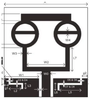
Fig. 4.1 Geometry of the notch elements: (a) shaped slot, (b) Inverted U-shaped slot, and (c) M-U-shaped resonant ... 95
Fig. 4.3 Geometry of the proposed antenna: (a) UWB antenna, (b) Single, (c) Dual, (d) Triple, (e) Quardruple, and (f)
Quintuple-band-notched antennas ... 100 Fig. 4.4 Simulated reflection coefficients |S11| of the
quintuple-band-notched antenna with different W3 values ... 102 Fig. 4.5 Simulated reflection coefficients |S11| of the
quintuple-band-notched antenna with different L3 ... 103 Fig. 4.6 Simulated reflection coefficients |S11| of the
quintuple-band-notched antenna with different L6 values ... 104 Fig. 4.7 Simulated reflection coefficients |S11| of the
quintuple-band-notched antenna with different L9 values ... 104 Fig. 4.8 Simulated reflection coefficients |S11| of the
quintuple-band-notched antenna with different W21values ... 105 Fig. 4.9 Simulated reflection coefficients |S11| of the
quintuple-band-notched antenna with different L12 values ... 106 Fig. 4.10 Simulated reflection coefficients |S11| of the
quintuple-band-notched antenna with different L15 values ... 106 Fig. 4.11 Simulated suface current distributions of the
quintuple-band-notched antenna at different frequncies (a) 2.45, (b) 3.54, (c)
5.49, (d) 7.53, (e) 8.47, (f) 3, (g) 6, and (h) 10 GHz ... 108 Fig. 4.12 Simulated imput impedance of the quintuple-band-notched antenna ... 111 Fig. 4.13 An approximated equivalent circuit of the quintuple-band-notched
antenna ... 111 Fig. 4.14 Transmission line model of the quintuple-band-notched antenna at
(a) Passband frequencies, (b) The first notched-band, (c) The second notched band, (d) The third notched band, (e) The
fourth notched band, and (f) The fifth notched band ... 113 Fig. 4.15 Front and back view of the prototyped proposed UWB monopole
antenna (a) Without, and (b) With band-notched ... 114 Fig. 4.16 Simulated and measured reflection coefficients |S11| of the
proposed antenna without band-notched ... 115 Fig. 4.17 Simulated and measured reflection coefficients |S11| of the
quintuple-band-notched antenna ... 116 Fig. 4.18 Simulated co-polarized without (red solid line) and with
radiation patterns of the proposed antenna at (a) 2.45, (b) 3.54,
(c) 5.49, (d) 7.53, and (e) 8.47 GHz ... 119 Fig. 4.19 Simulated overall/total efficiency of the quintuple band notched
antenna ... 120 Fig. 4.20 Simulated and measured maximum realized gain values of the
quintuple-band-notched monopole antenna ... 120 Fig. 4.21 Simulation setup of the antenna for the time-domian investigation ... 121 Fig. 4.22 Simulated signals of the antenna with/without notch with single
impulse input signal for the side by side case ... 122 Fig. 4.23 Simulated signals of the antenna with/without notch with single
impulse input signal for the face to face case ... 123 Fig. 5.1 Geometries of Four different CSRR filter structures ... 130 Fig. 5.2 Simulated reflection coefficients |S11| of the antenna for different
structures ... 131 Fig. 5.3 Simulated reflection coefficients |S11| of the antenna for different
values (a) W2, and (b) L2 ... 132 Fig. 5.4 Topology of three pairs of switches on the radiator: Ws= 0.8 mm ... 133 Fig. 5.5 Simulated current distributions: (a) S2 OFF at 5.45 GHz, (b) S2 ON
at 5.45 GHz (UWB state), and (c) S2 OFF at 8.5 GHz ... 134 Fig. 5.6 Simulated input impedance of the antenna (Structure 3) ... 135 Fig. 5.7 Transmission line model for (a) CSRR structures with switches ON
(passband), (b) CSRR structures with switch S3 OFF, (c) CSRR structures with switch S2 OFF, and (d) CSRR
structures with switches S2 and S3 OFF ... 136 Fig. 5.8 Selected prototypes of the proposed antenna for five switching states ... 137 Fig. 5.9 Simulated and measured reflection coefficients |S11| of the proposed
antenna for switching States 1-5 ... 141 Fig. 5.10 Simulated reflection coefficients |S11| of the proposed antenna for
switching States 6-8 ... 142 Fig. 5.11 Simulated co-polarization (red solid line) and cross-polarization
(red break line), and measured co-polarization (blue dot line) and cross-polarization (blue dot break line) radiation patterns of the proposed antenna at (a) 2.4 GHz (State 5), (b) 3.57 GH
(c) 5.5 GHz, and (d) 8.5 GHz ... 144 Fig. 5.12 Measured gains of the proposed antenna for five different
Fig. 5.13 Simulated overall/total efficiency of the antenna for five different
switching states ... 145
Fig. 5.14 Simulated signals of the antenna with single impulse input signal for switching States 4 and 5 in the side by side case ... 147
Fig. 5.15 Simulated signals of the antenna with single impulse input signal for switching States 4 and 5 in the face to face case ... 147
Fig. 6.1 Geometry of the proposed UWB-MIMO monopole antenna (Antenna 1): Front view (up) and Back view (down) ... 152
Fig. 6.2 Simulated and measured S parameters of Antenna 1 (without slots) ... 153
Fig. 6.3 Simulated S21 of Antenna 1 with different Wd values ... 155
Fig. 6.4 Simulated current distributions of Antenna 1 at: (a) 3.1, and (b) 10.6 GHz. Port 1 is excited; Port 2 is terminated with a 50 Ω load ... 156
Fig. 6.5 Geometry of the modified UWB-MIMO monopole antenna with the trident-like slot (Antenna 2) ... 157
Fig. 6.6 Simulated S parameters of Antenna 2 ... 159
Fig. 6.7 Simulated surface current distributions of Antenna 2 with at the frequencies of: (a) 3.1 GHz, (b) 10.6 GHz. ... 160
Fig. 6.8 The approximate equivalent circuit of Antenna 2 ... 161
Fig. 6.9 Simulated S parameters of Antenna 2 for different W1 values ... 163
Fig. 6.10 Simulated S parameters of Antenna 2 for different L1 values ... 164
Fig. 6.11 Simulated S parameters of Antenna 2 for different L2 values ... 165
Fig. 6.12 Simulated S parameters of Antenna 2 for different W3 values ... 166
Fig. 6.13 Prototype of the modified UWB-MIMO antenna (Antenna 2) ... 168
Fig. 6.14 Simulated and measured S parameters of Antenna 2 (with slots) ... 169
Fig. 6.15 Measured radiation patterns of Antenna 2 at the frequencies of ... 170
Fig. 6.16 Simulated and measured gains of the antenna with and without slot ... 171
List of Tables
Table 2-1 Comparison of various SWB antennas ... 28
Table 2-2 Comparison of multiple band-notched UWB antennas ... 37
Table 2-3 UWB antennas with reconfigurable band-rejection ... 43
Table 2-4 Summarized states of the art on UWB-MIMO antennas ... 52
Table 2-5 Design consideration for UWB-MIMO antennas ... 54
Table 3-1 Optimized parameters of the SWB antenna in Fig. 3.9 ... 78
Table 3-2 Comparion of the analyze performanes for three antennas ... 83
Table 4-1 Numerical and theoretical predictions for the band-notched frequency ... 97
Table 4-2 Dimensions in mm of the antenna shown in Fig. 4.3(a) ... 100
Table 4-3 Dimensions in mm of MSRs for the quintuple-band-notched antenna shown in Figs. 4.3(b-f) ... 101
Table 4-4 Calculated fidelity factor for UWB antenna without and with band-notched function ... 123
Table 4-5 Comparison with the design in [75] ... 125
Table 5-1 Numerical and theoretical predictions for the band-notched frequency ... 130
Table 5-2 Switch combinations and operational frequency bands for each state ... 139
Table 5-3 Calculated fidelity factor of the UWB antenna for switching States 4 and 5 ... 146
Abstract
This thesis focuses on four inter-related research topics on the design and analysis of compact planar ultra wide-band (UWB) monopole antennas for future wireless communications, namely, a planar super-wide-band (SWB) monopole antenna, a planar UWB antenna with band-notched characteristics, a planar UWB antenna with reconfigurable band-rejection features, and a planar UWB multiple-input and multiple-output (MIMO) antenna.
A novel Mickey-mouse shaped planar monopole antenna with SWB performance is proposed and investigated. Three different techniques for bandwidth enhancement are implemented. The antenna is evolved from the traditional circular monopole antenna and has achieved an impedance bandwidth of more than 100:1 and a stable radiation patterns over a wider bandwidth.
The design of a compact planar UWB monopole antenna (22 × 34 mm2), incorporated with five m-shaped resonators (MSRs) at different positions, to achieve quintuple-band-notched performance is presented. The frequency-domain performance (in term of reflection coefficients, realized gain, efficiency, and radiation pattern), and time-domain performance (in term of pulse responses and fidelity), are investigated by simulation and measurement. The results show that the proposed UWB antenna has approximately omnidirectional radiation patterns and excellent band-notched behaviours and good time domain performance with the fidelity of more than 85.5% in the pulse response.
reconfigurability. The proposed antenna can operate at different switching states including a UWB state, single and dual band-notched states with good rejection behaviours. Good radiation patterns and gain values are also obtained for different switching states. This compact wideband antenna can be very good candidate for a wide range of mobile portable applications.
A compact planar UWB-MIMO antenna (60 × 45 mm2) is presented for wireless applications. The wideband isolation of more than 15 dB is achieved by etching a new trident-like slot on the ground plane of the antenna. An equivalent circuit have been introduced for analysis and the diversity performances are studied. The results show that the proposed MIMO antenna is a very good candidate for wireless applications.
CHAPTER 1
INTRODUCTION
1.1
Research Motivations
Many emerging wireless communication systems are aimed at providing higher data-rate transmission and more versatile services. The dramatically advancement in the wireless communication systems and the substantially increasing demand from the consumers have pushed the radio system approaching its physical limit.
antenna (PMA) has attracted the most attention due to its low profile, low cost, simple fabrication, omni-directional radiation pattern and ease of integration with RF front end [10,11].
1.1.1
A Super Wideband Antenna (SWB) Planar
Monopole Antenna
Various wideband antennas have been interesting subjects and have found important applications in military and civilian systems. The PMA has been a good candidate for such applications. There has been a question of how wide the bandwidth of a PMA could be. Can we make a PMA a SWB antenna? SWB technology could possibly be a potential approach to offer high-resolution sensing applications such as the ground-penetrating radar and through wall sensing. SWB radio technology has unique advantages as compared to narrowband technology, and also comprised all UWB technology features but with more channel capacity, higher precision and supper resolution in communications and ranging. Therefore, design of a compact planar monopole antenna with SWB performance is the first research topic in the thesis.
1.1.2
A Planar UWB Antenna with
Quintuple-Band-Notched Characteristics
GHz (5.15-5.35 GHz) and 5.75-GHz (5.725-5.825 GHz), the Worldwide Interoperability for Microwave Access (WiMAX) systems operating in the 2.35 GHz (2.3-2.4 GHz), 2.6 GHz (2.5-2.69 GHz), 3.35 GHz (3.3-3.4 GHz), 3.5 GHz (3.4-3.6 GHz), 3.7 GHz (3.6-3.8 GHz) and 5.8 GHz (5.725-5.85 GHz) bands, downlink of X-band satellite communication system operating at the band of 7.25-7.75 GHz and ITU band of 8.01-8.5 GHz respectively. The relative power-spectrum density (PSD) in the UWB and some existing narrowband communication systems is shown in Fig. 1.1.
Fig. 1.1 Power spectrum density of UWB and some narrow-band communication systems
UWB monopole antenna with multiple-band-notched characteristics and good level of rejections is the second research topic in the thesis.
1.1.3
A Planar UWB Reconfigurable Band Rejection
UWB Antenna
Antennas are required to support multiple standards and application since the demand of compactness of the systems and devices. To achieve this, reconfigurable antennas, incorporating switches become a promising solution. In the meantime, for the future UWB system, there is a need for band rejection capabilities to avoid interfering with nearby narrow band communication systems such as WLANs and WiMAX, etc. In this condition, a planar UWB antenna with reconfigurable band-notched capability could be useful.
1.1.4
A Planar UWB-MIMO Antenna for Wireless
Applications
which can dramatically degrade the MIMO system performance. Therefore, the fourth research topic of the thesis is to design a planar UWB-MIMO antenna with compact structure and an optimised minimum mutual coupling that cover the entire range of the UWB band.
1.2
Organization of the Thesis
This thesis is organised in seven chapters as follows:
Chapter 2 reviews the development of the UWB/SWB antennas in past decades. The state-of-the-art technology of band-notched UWB antennas is also presented. Previous work on wideband to band-rejection reconfigurable antennas and UWB-MIMO antennas for wireless applications are also compared and summarised.
Chapter 3 presents a new compact planar monopole antenna with SWB performance. Additionally, the radiation mechanism of the planar SWB monopole antenna is also investigated.
In Chapter 4, the operating principles of the M-shaped resonators (MSRs) are studies. The use of the MSRs to create a UWB monopole antenna with quintuple-band-notched characteristics is proposed. The performances of the proposed antenna in the frequency-domain and time-domain are also investigated.
Chapter 6 presents a compact UWB-MIMO antenna for wireless applications. A novel approach to enhance the wideband isolation of the two antenna ports/elements is introduced and investigated. The proposed design concept is verified using both numerically and experimentally methods.
Finally, Chapter 7 finalises the thesis, reviews the work undertaken and draws main conclusions of the research, it is finished by suggesting some future work.
1.3
Key Contributions
The major contributions in this thesis are highlighted in the following sections.
Chapter 3: A Compact Super Wideband (SWB) Planar
Monopole Antenna
A novel compact Mickey-mouse shaped planar monopole antenna with SWB performance is proposed and investigated. Three different techniques for bandwidth enhancement are implemented. The SWB antenna is evolved from the traditional circular monopole antenna and has achieved an impedance bandwidth of more than 50:1 and exhibited a wide band pattern characteristics, the usable spherical patterns are sustained in a bandwidth wider than 10:1 (the work was published in [12]).
Chapter 4: A Compact UWB Antenna with
Quintuple-Band-Notched Characteristics
systems. A newly compact planar UWB monopole antenna with quintuple-band-notched characteristics is proposed and investigated. The size of the antenna is 22 × 34 mm2, which is about 10% smaller compared to the design in the literature; the band-notched functions are successfully achieved by integrating five half/one-wavelength MSR structures into the radiator, feed-line, and ground plane. And excellent levels of rejection in the notched bands are achieved. It can be also confirmed that the proposed antenna has limited effect on the time-domain performances (the work was submitted as listed in Section 1.4.1).
Chapter 5: A UWB Antenna with Reconfigurable
Band-Rejection Characteristics
A novel planar UWB monopole antenna with reconfigurable narrow band-rejection characteristic is proposed and studied. Both the numerical and experiment results are confirmed that the proposed antenna has a capability of switching independently ON and OFF for different states including a UWB state, single and dual band-notched states with better band-rejection behaviours compared to designs in the literature. It is evident that the performances have verified the proposed design concept (the work was submitted as listed in Section 1.4.2).
Chapter 6: A Compact UWB-MIMO Antenna for Wireless
Applications
dB is achieved for the operating frequency from 2.3 to 12 GHz. The numerical and experimental results are indicated that the antenna has a very good diversity performance (the work was submitted as list in Section 1.4.3).
1.4
List of Publications
1. P. Cao, Y. Huang, J. W. Zhang, R. Alrawashdeh and X. Zhu, “A UWB planar monopole antenna with quintuple-band-notched characteristics,”
submitted to IET Microwaves, Antennas & Propagation. 2013.
2. P. Cao, Y. Huang, R. Alrawashdeh, J. W. Zhang and X. Zhu, “A UWB monopole antenna with reconfigurable band-notched characteristics,”
submitted to International Journal of Antennas and Propagation. 2013. 3. P. Cao, Y. Huang, J. W. Zhang, N. Khiabani and X. Zhu, “A
UWB-MIMO monopole antenna for wireless communications,” submitted to IET Microwaves, Antennas & Propagation. 2013.
4. P. Cao, Y. Huang, J. W. Zhang and R. Alrawashdeh, “A compact super wideband monopole antenna,” in 7th European Conference on Antennas and Propagation (EuCAP), Sweden, pp. 3107-3110, 2013.
5. P. Cao, Y. Huang and J. W. Zhang, “A UWB monopole antenna for GPR application,” in 6th European Conference on Antennas and Propagation (EuCAP),Prague,pp. 2837-2840, 2012.
6. P. Cao, Y. Huang, J. W. Zhang and Y. Lu, “A comparison of planar monopole antennas for UWB applications,” in Antennas and Propagation Conference (LAPC), Loughborough, pp. 1-4, 2011.
to International Conference on Electromagnetics in Advanced Applications, IEEE-APS Topical Conference on Antennas and Propagation in Wireless Communications, Torino, Italy, pp. 12-17 Sep., 2011.
8. Y. Lu, Y. Huang, H. T. Chattha and P. Cao, “Reducing ground-plane effects on UWB monopole antennas,” IEEE Antennas and Wireless Propagation Letters, vol. 10, pp. 147-150, 2011.
9. J. W. Zhang, Y. Huang, P. Cao and H. T. Chattha, “Broadband unidirectional dipole antennas for wireless applications,” in Antennas and Propagation Conference (LAPC), Loughborough, pp. 1-4, 2011.
10. J. W. Zhang, Y. Huang, and P. Cao, “Harvesting RF energy with rectenna arrays,” in 6th European Conference on Antennas and Propagation (EuCAP),Prague, pp. 365-367, 2012.
11. J. W. Zhang, Y. Huang and P. Cao, “A wideband cross dipole rectenna for wireless harvesting,” in 7th European Conference on Antennas and Propagation (EuCAP), Sweden, pp. 3063-3067, 2013.
12. R. Alrawashdeh, Y. Huang and P. Cao, “A conformal U-shaped loop antenna for biomedical applications,” in 7th European Conference on Antennas and Propagation (EuCAP), Sweden, pp. 157-160, 2013.
1.5
References
[1] Federal Communications Commission, “Revision of Part 15 of the commission’s rules regarding ultra-wideband transmission systems, first report and order,” ET Docket 98-153, FCC 02-48, pp. 1-118, Feb.14, 2002.
[2] N. P. Agrawall, G. Kumar, and K. P. Ray, “Wide-band planar monopole antennas,” IEEE Trans. on Antennas and Propagation, vol. 46, pp. 294-295, 1998.
[3] E. S. Angelopoulos, A. Z. Anastopoulos, D. I. Kaklamani, A. A. Alexandridis, F. Lazarakis, and K. Dangakis, “Circular and elliptical CPW-fed slot and microstrip-fed antennas for ultra-wideband applications,” IEEE Antennas and Wireless Propagation Letters, vol. 5, pp. 294-297, 2006.
[4] H. D. Chen and H. T. Chen, “A CPW-fed dual-frequency monopole antenna,” IEEE Trans. on Antennas and Propagation, vol. 52, pp. 978-982, 2004.
[5] Y. Lu, Y. Huang, Y. C. Shen, and H. T. Chattha, “A further study of planar UWB monopole antennas,” in Antennas & Propagation Conference, 2009. LAPC. Loughborough, pp. 353-356,2009.
[6] L. Paulsen, J. B. West, W. F. Perger, and J. Kraus, “Recent investigations on the volcano smoke antenna,” in IEEE Antennas and Propagation Society International Symposium, vol. 3, pp. 845-848, 2003.
[8] K. C. L. Chan; Y. Huang, X. Zhu, “A planar elliptical monopole antenna for UWB applications,” in IEEE/ACES Inter. Conference on Wireless Communications and Applied Computational Elec., Hawaii, U.S.A., pp. 182-185, Apr. 3-7, 2005.
[9] J. X. Liang, C. C. Chian, X. D. Chen, and C. G. Parini, “Study of CPW-fed circular disc monopole antenna for ultra-wideband applications,” in
IEE Proc. Microwaves, Antennas and Propagation, pp. 520-526, Dec. 2005.
[10] Z. N. Chen, et al, “Planar antennas,” IEEE Microwave Magazine, vol. 7, issue 6, pp. 63-73, Dec. 2006.
[11] Y. Huang and Kevin Boyle, “Antennas from theory to practice,” John Wiley and Sons, 2008.
CHAPTER 2
BACKGROUND
2.1
Development of UWB/SWB Antennas
2.1.1
Definition of UWB
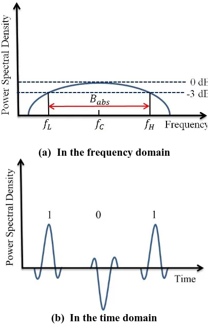
Babs fH fL
(2.1) Q 1 ) f f ( ) f f ( 2 f B FBW L H L H C abs
(2.2)
where 𝑓𝑐 is the centre frequency and Q is defined as quality factor, which is inversely proportional to the half power fractional bandwidth of the antenna. In general, an antenna is a resonate device. If the antenna can be well matched to its feed across a certain frequency range, that frequency range is defined as it impedance bandwidth. The impedance bandwidth can be specified in terms of return loss (S parameters) over a frequency range. Generally, in the wireless communications, the antenna is required to provide a return loss great than 10 dB over its frequency bandwidth.
(a) In the frequency domain
[image:30.595.217.420.374.695.2](b) In the time domain
The frequency-domain and time-domain behaviours of a UWB communication system are illustrated in Fig. 2.1. Signals which occupy an extremely wide bandwidth in the frequency domain are usually very short pulses in the order of sub-nanosecond in the time domain. Thus, the most significant difference between traditional radio transmissions and UWB radio transmissions is that the traditional systems employ carrier-wave modulation, while UWB system transmits information by generating radio energy as very narrow pulses occupying a large spectrum.
The suitability of UWB signals for high-speed data communications can be obtained from the Shannon capacity formula [2]. For an ideal additive white Gaussian noise (AWGN) channel with limited bandwidth, the maximum achievable data rate can be calculated by.
) 1
(
log2 SNR B
C (2.3)
where C denotes the channel capacity (maximum transmit data rate), B stands for the bandwidth of the channel. SNR is the signal-to-noise ratio (SNR) over the entire channel bandwidth Equation (2.3) indicates that it becomes possible to transmit more information from transmitter to the receiver by increasing the bandwidth occupation or transmission power. However the transmission power in a wireless communication system is limited because of the regulation limit or due to the fact that many portable devices and systems are battery powered and the potential interference should also be avoided. Therefore, a wide frequency bandwidth is the solution to increase its channel capacity.
(EIRP) level to -41.3dBm/MHz (known as Part 15 Limit) [3]. Fig. 2.2 shows the spectral masks of FCC’s regulation for UWB communication systems [4].
(a) Indoor limits
(b) Outdoor limits
2.1.2
UWB/SWB Antennas
UWB antennas usually are referred to as the antenna with an actual frequency range from 3.1 to 10.6 GHz with a ratio bandwidth of 3.4:1, which the antenna with a ratio bandwidth not less than 10:1 is generally called the SWB antenna [5]. In this section, the developments of UWB/SWB antennas are reviewed.
The earliest antenna with wideband properties was the biconical antennas made by Sir Oliver Lodge in [6], as shown in Fig. 2.3. At the early stage, the antennas were based on three-dimensional structures with bulky volumes such as biconical/conical antennas [7], spheroidal antenna [8-9], omni-directional and directional coaxial horn antenna [10]. Some of the very early wideband antennas are shown in Fig. 2.4.
(a) Biconical (left)/conical(right) antennas (1939) [7]
(b) A spheroidal antenna (1941) [8, 9]
(c) A omni-directional (left), and directional (right) coaxial horn (1948) [10]
In the late 1950 and early 1960, a family of antennas with a ratio bandwidth more than 10:1 were first developed by Rumsey et al, which were called as the frequency independent antenna [5]. Classical shapes of such antennas include the equiangular spiral antenna and the planar log-periodic dipole antennas, as shown in Fig. 2.5.
(a) An equiangular spiral antenna (left) and (b) Log-periodic dipole antenna (right) (1959) [5]
Fig. 2.5 Some frequency independent antennas
From 1990s, many new-style SWB antennas have been proposed, which can be summrized as three types [11]: The SWB metal-plate monopole antennas, prited slot antennas and planar monopole antennas. The details of these types of the SWB antennas are reviewed and compared below.
2.1.2.1
SWB Metal-plate Monopole Antennas
2.6(a). The antenna achieved an impedance bandwidth ratio of more than 10:1 and a radiation pattern bandwidth of 4:1. Later on in [16], the leaf-shaped plate monopole antenna comprised of three circular holes with the dielectric layer, which provides the impedance bandwidth ratio better than 20:1 from 1.3 to 29.7 GHz, as shown in Fig. 2.6(b). In the meantime, the radiation pattern bandwidth has extended due to the introduction of three circular holes.
(a) (b)
Fig. 2.6 The metal-plate monopole antenna: (a) Planar inverted cone antenna (2004) [15], and (b) Leaf-shaped plate antenna (2006) [16]
(a) (b)
Fig. 2.7 The rectangular metal-plate monopole antenna (a) Offset feed (2001) [17], and (b) Short post and bevelling (2004) [19]
2.1.2.2
SWB Slot Antennas
SWB slot type antennas were also proposed and investigated [20-26] in the past decades. These antennas can be mainly divided in two categories, such as SWB tapered slot and wide-slot antennas.
SWB Tapered-slot Antennas
The conventional Vivaldi antenna typically has a bandwidth of less than 3:1,
(a) (b)
Fig. 2.8 The balanced antipodal Vivaldi antenna (a) Convectional microtrip feed (1988) [20], and (b) CPW feed (1993) [21]
SWB Wide-slot Antennas
In recent years, various SWB printed wide-slot antennas have been reported to use different slot shapes [22-25]. As stated in [22], the printed slot antenna using U-shaped microstrip feeding was studied by adding a tuning rectangualr cooper pad in one side of the mircrostrip (to improve the impenance bandwidth of the antnena). By properly tuning the physial size of the copper pad, The antenna achieved a fractional bandwidth of more than 135.7%, covering frequencies from 2.3 to 12 GHz and a gain variation from 2 to 7 dBi was obtained, as shown in Fig. 2.9.
The impedance bandwidth of slot antenna was further improved. As shown in Fig. 2.10, the design of using Planar Invested Cone Antenna (PICA) like structures was proposed and the antenna achieves a ratio bandwidth of 13:1, covering frequencies from 2.2 to 30 GHz [23].
Fig. 2.10 The PICA slot antenna (2008) [23]
Apart from Microstrip line-fed, the CPW-fed printed wide-slot antennas also have been designed to demenstrate a wide bandwidth capability. For instantace, in ref [24], the elliptical slot antenna with an elliptical patch as the feed has a ratio bandwidth about 15:1, covering frequenies from 1.3 GH to 20 GHz, as shown in Fig. 2.11.
Another type of printed slot antenna is printed bow-tie slot antenna and the bow-tie slot is added under the bow-tie slot antenna [25], which has a simple configuration, wider bandwidth, lower cross-polarization levels and higher gain performance, as shown in Fig. 2.12.
Fig. 2.12 The bow-tie slot antenna (2004) [25]
2.1.2.3
SWB Planar Monopole Antennas
During the past few year, many planar monopole antennas fed by the mircrostrip (MS)-line [26-29] and the CPW [30-32] have been also proposed for SWB applications. Because of this attractive features such as low profile, low-cost, ease of fabrication and omni-directional radiation pattern. Various planar monopole antennas fey by the MS line and CPW are reviewed as follows:
SWB Microstrip-fed Monopole Antennas
Fig. 2.13 The planar circular asymmetrical dipole antenna (2010) [26]
In [27], a wideband monopole fractal antenna with Hilbert fractal slot patterned ground plane was also investigated, as shown in Fig. 2.14. The radial arrow fractal slots cause the path lengths of the surface currents on the radiator to have the multiband behavior. The antenna has a wide bandwidth ranging from 1.65 to 14.6 GHz or a ratio bandwidth about 14:1 for S11 < -10 dB and a stable gain performance about 3 dBi across the desired band were obtained. Recently, another circular-hexagonal fractal antenna was proposed in [28] with a much wider bandwidth ranging from 2.18 to 44.5 GHz.
[image:41.595.248.391.532.690.2]In the meantime, another planar microstrip-fed monopole antenna to achieve super wideband performance was proposed in [29], as shown in Fig. 2.15. The introduction of the semi-elliptically fractal-complementary slot was to reduce the ground plane effect by suppressing the electric currents on the ground plane at lower end frequency. Thus, a -10 dB bandwidth of 172% (1.44-18.8 GHz) is achieved with a ratio bandwidth 12:1. Near omni-directional radiation characteristics were observed at the lower frequency bands and the cross-polarization level rises with increasing frequency and the measured gain values were obtained from 1 to 7 dBi.
[image:42.595.246.393.312.491.2]Recently, in [30], a compact implementation of a microstrip-fed monopole antenna for the SWB communications was proposed, as shown in Fig. 2. 16. The proposed antenna possessed a broad frequency range from 3 to 33 GHz or a ratio bandwidth of 11:1, but also implemented with switchable dual band-notched characteristics.
SWB CPW-fed Monopole Antennas
Apart from Microstrip line-fed, the CPW-fed monopole antennas with SWB perforamne have also been investigated. A compact CPW-fed monopole antenna composed of an elliptical monopole patch and a coplanar trapeziform ground plane was introduced in [31], as shown in Fig. 2.17(a). The results demonstrate that this antenna achieves a ratio impedance bandwidth of 21.6:1, covering frequency range from 0.41 to 8.86 GHz, with a good gain and omni-directional radiation performance as well.
(a) (b)
Fig. 2.17 The CPW-fed planar monopole antenna: (a) Elliptical (2007) [31], and (b) Trapezoid (2010) [32]
More recently, in [33], a SWB antenna with the impedance bandwidth from 5 to 150 GHz or a ratio bandwidth of 30:1 was successfully developed, as shown in Fig. 2.18.
Fig. 2.18 The newly developed CPW-fed planar monopole antenna [33]
Table 2-1 Comparison of various SWB antennas
Antenna Type
Bandwidth (GHz) (S11 <-10 dB)
Ratio Bandwidth (S11 <-10 dB)
Size (
2)Gains (dBi) Trapezoidal
metal plate monopole [14]
1.07 - 12.2 11.4:1 0.89 0.89 0.5- 4.5 Leaf-shaped
plate monopole [16]
1.3 - 29.7 22.8:1 0.35 0.35 3-5
Tapered slot
antenna [21] 1 - 18 18:1 0.43 0.32 3.2-9
CPW-fed rectangular slot
antenna [24]
1.3 - 20 15:1 0.39 0.39 ---
A circular-hexagonal Fractal antenna
[28]
2.18-44.5 20.4:1 0.330.23 2-3
MS-fed elliptical
egg-shape planar monopole antenna[29]
1.44-18.8 12:1 0.37 0.21 1-7
CPW-fed planar monopole antenna [33]
5-150 30:1 0.250.28 ---
2.2
Review of Band-Notched UWB Antennas
2.2.1
Survey on Techniques to Generate Notched
Characteristics
[image:46.595.221.419.442.590.2]Several designs have been proposed to use planar UWB antennas to obtain the band-notched function [34-75]. Amount the proposed methods, the most widely used approaches can be classified into few groups according to the resonator structures positions on the antenna such as on or next to the radiator or other side of the substrate or the feed line or the top edge of the ground plane, as shown in Figs. 2.19(a) to (c), respectively. In the literature, various techniques have been applied to obtain the single band-notched characteristics of UWB antennas. The details of these techniques can be summarised as follows.
Fig. 2.19 Possible postions of the resonat strucure on UWB antenna
2.2.1.1
Inserting slots
line were demonstrated to create band notched functions. Generally speaking, the notched frequency is determined by the total length of the slot or cut which is approximately half or quarter wavelength. Some of these designs are now described in detail below.
In [34], a CPW-fed compact elliptical monopole UWB with a narrow frequency rejection was presented. The frequency band-notched at 5.65 GHz was achieved by inserting two inverted half-wavelength L slots near the CPW feeding on the ground plane/radiator of the antenna, respectively, as shown in Fig. 2.20(a). The principle of this approach was to stop the current flow at the introduction of the inverted L slots, which the radiation of the antenna could be suppressed and a notched frequency could be created.
Fig. 2.20 (a) A CPW UWB antenna integrated with two inverted L slots: On the ground plane (left) and on the radiator(right) [34]
Fig. 2.20 (b) Simulated radiation patterns of the slot on the radiator and ground plane
A CWP-fed compact elliptical UWB monopole antenna with a U-shaped and C-shaped slot in the patch was introduced in [35], as shown in Figs. 2.21(a) and (b), respectively. The band rejection was caused by the presence of a slot having a length of approximately/2 at the frequency of 5.8 GHz and the values of gain reduction were 10 dB and 5 dB, respectively.
(a) (b)
Ref. [41] introduced the use of a pair of meander grounded stubs to design a deep single band-notched UWB planar monopole antenna, as shown in Fig. 2.22. The results showed that the single band notch was achieved from 5.15 to 5.825 GHz with gain suppression of 9 dB.
Fig. 2.22 A MS-fed UWB antenna integrated with a pair of ML [41]
A compact UWB monopole antenna [42] in Fig. 2.23 obtained the frequency band-notched function by inserting a CPW resonant cell on the feeding line. Measured results indicated that the antenna has a notched band from 5.10 to 5.94 GHz.
[image:49.595.254.384.516.675.2]2.2.1.2
Parasitic Element
The parasitic strips have also been used to achieve band rejection function [43-46]. For example, in [43], a UWB antenna with band-notched function was investigated by placing a pair of parasitic elements in the radiating aperture of the planar antenna at the top and bottom layer, as shown in Fig. 2.24(a). The results showed that the antenna exhibits a 10 dB return loss bandwidth from 3 to 11 GHz with 9 dB gain suppression at the rejection bands.
Another example is a CPW-fed UWB elliptical monopole [44] with two resonating inverted L-shaped stubs are collected to the radiator, as shown in Fig. 2.24(b). The band-notched was realized at the center frequency of 5.5 GHz with only 5 dB gain suppression.
(a) Half circle shape [43] (b) Elliptical [44]
Fig. 2.24 The UWB antennas integreated with parasitic strips
Fig. 2.25 A UWB antenna integrated with an extended strip and a loaded strip [47]
2.2.1.3
Split-Ring-Resonant (SRR) or Complementary SRR
(CSRR)
SRR, originally proposed by Pendry [48], can be considered as an electronically small size resonator with a very high quality (Q) factor [49], which is able to produce a band-notch property for UWB antennas [49, 50]. Ref. [49] introduced a UWB antenna with a modified SRR slot- type structure on the path for rejecting unwanted frequency band, as shown in Fig. 2.26. The results showed that the antenna has a notched band at the center frequency of 5.2 GHz. The value of gain suppression was about 9 dB. In addition, [51] was successfully achieved a single band-notched function for WLAN band at 5.7 GHz.
2.2.1.4
Open-loop resonant
An open-loop resonator was placed onto the other side of the substrate and a dual-gap open-loop resonator was inserted into the radiating element of a UWB monopole antenna, were studied in [52-53], and shown in Figs. 2.27(a) and (b), respectively. By printing the open-loop on the reverse side of the substrate, the antenna yielded almost 11 dB gain suppression at the notched center frequency of 5.2 GHz. For the case of etching the dual-gap open loop resonator into the radiator, the notch band was achieved at 4.2 GHz with 5.8 dB gain suppression.
(a) (b)
Fig. 2.27 The UWB antenna with (a) An open-loop resonator [52], and (b) A dual-gap open-loop resonator [53]
2.2.1.5
Electromagnetics Band Gap (EBG)
had a notch band at 5.5 GHz. The gain value was not presented in the paper. It had limited band-notched performance due to the dielectric loss of the substrate.
(a) (b)
Fig. 2.28 A UWB antenna with (a) EBG structure [54], (b) Unit cells of EBG [54] and (b) Equivalent circuit of the EBG [54]
Though lots of band-notched UWB antennas have been reported in [33-54], most of them were designed to achieve one band-notched function with a reasonable rejection performance. In order to mitigate the interference by several existing narrow band communication systems, a wide variety of multiple band-notched UWB antennas have been designed and reported in [55-75]. These designs with two [55-64], three [65-71], four [72-74], and five [75] band-notched functions were achieved by utilizing some of the described techniques. The details of these designs are summarized in Section 2.2.2.
2.2.2
Comparison of Different Approaches
Table 2-2 Comparison of multiple band-notched UWB antennas
Ref .
Antenna
Layout Techniques
Analyzed Parameters Gain Suppression (dB) Notch Bands (GHz)
[55] EBG
Size: 3442.5 mm2 BW: 2.27-10.83 GHz 7.5 5.2 3.37-3.87 5.32-6.15 [56] R-shaped stub and G
stub
Size: 24 36 mm2 BW: 3-12 GHz
8 6 5.15-5.35 5.72-5.82 [57] R-shaped stub and
G-slot DGS
Size: 20 25 mm2 BW: 2.8-11.8 GHz
5 7.4
3.3- 3.8 5.1-6
[58] C-shaped
slots
Size: 3026 mm2 BW: 3.1-10.6 GHz
8 7
3.3-3.8 5-6
[59] Adding strips Size: 30 35 mm 2 BW: 2.3-6 GHz
9 6 2.5-2.7 3.3-3.8 [60] Etching two square CSRRs
Size: 30 34 mm2 BW: 3-11 GHz
3 4 3.4-3.6 5.1-5.9 [61] Folded stepped impedance resonator
Size: 25 33 mm2 BW: 3.07-10.61 GHz 9 9.5 3.41-3.68 5.37-6.01
[62] SRRR and
slots
Size: 18 30 mm2 BW: 2.38-12 GHz
11 7
[63] Open-ended thin slits
Size: 35 35 mm2 BW: 3-11 GHz
8 6
5.15-5.35 5.725-5.825
[64] Strips Size: 24 29 mm
2 BW: 3 - 11 GHz
17 18
3.0-3.6 5.1-6.1
[65] SRRs Size: 54 47 mm
2 BW: 2.1-10.5 GHz
9 7 7.5 2.24-2.62 3.78-4.03 5.94-6.4
[66] Closed-loop
slots
Size: 25 30 mm2 BW: 3.02-11 GHz
14 8 7 3.3-3.6 5.15-5.35 5.725-5.825
[67] Meandered
lines
Size: 30 39.3 mm2 BW: 2.68 -11.15
GHz 7 6 5.8 3.3-3.6 5.15-5.35 5.725-5.825 [68] Closed-loop ring resonators
Size:33 30 mm2 BW: 2.8-11 GHz
7 5 5 3.3-3.7 5.15-5.35 5.725-5.825
[69] Parasitic
strips
Size: 30 22 mm2 BW: 2.92-15.7 GHz
6 8 7 2.26-3.71 5.15-5.37 5.78-5.95 [70] Capacitive load loop (CLL)
Size: 27 34 mm2 BW: 2.8-11 GHz
8 8 6 3.3-3.6 5.15-5.35 5.725-5.825 [71] QW-stubs and open-ended slots
Size: 28 28.5 mm2 BW: 2.8-11 GHz
[72] CSRR Size: 31 31 mm 2 BW: 2.8 11.4 GHz
7 4.5 3.5 6 3.3-3.6 5.0-5.4 5.7-6.0 7.6-8.6 [73] Two C-shaped slots and inverted U-shaped
Size: 26 28 mm2 BW: 3.1-12 GHz
8 5 6 4 5.1-5.43 5.78-5.98 7.2-7.79 8.03-8.83
[74] U-shaped slot Size: 30 31 mm
2 BW: 2.8-12 GHz
10 6 7 7.5 3.5-3.6 4.5-4.8 5.15-5.35 5.725-5.825 [75] C-shape slots and Open-circuit stubs
Size: 2631.8 mm2 BW: 2.45-12 GHz
2.3
UWB Antennas with Reconfigurable Bands
Rejection
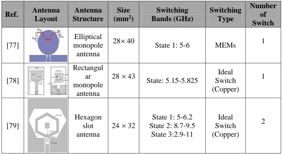
In Section 2.2, UWB antennas with fixed band-notched characteristics have been reviewed. In this Section, several UWB antennas with reconfigurable band rejection operation incorporating with the switches have been proposed [76-86] and are summarized in Table 2-3.
[image:57.595.245.401.413.545.2]In [77], the CPW-fed elliptical UWB monopole antenna was achieved to reject at 5.5 GHz by using MEMS switches to connect and disconnect the stubs into the radiator, as shown in Fig.2.29. The switching ON and OFF at single band rejection was proposed in [78] where a parasitic patch was added in the back of the rectangular monopole with an ideal switch to obtain the band notch.
Fig. 2.29 An elliptical UWB antenna with switchable stubs [77]
can be dynamically switching on/off by controlling the surface curents paths along the slits with eight PIN diodes. The PIN diodes effectively short circuit to the dielectric slits without affecting between the band notches.
Fig. 2.30 A UWB planar monopole antenna with multiple-band-rejection switchable capability [86]
In the literature, many papers also discussed UWB slot antennas with multiple modes bands-notched reconfigurable ability by incorporating ideal switches or PIN diodes [79, 81, 83-85].
Fig. 2.31 A UWB slot antenna with multi-band-rejection switchable capability [79]
[image:59.595.245.395.119.327.2]Furthermore in [84], a circular slot with tree arms on a radiating patch was introduced to improve the bandwidth of antenna and also to realize the switching functions, as shown in Fig. 2.33. By biasing two PIN diodes, the antenna achieved a UWB mode in the frequency range of 3.12-12.51 GHz, two single bands of 3.12-3.84 GHz and 5-6.07 GHz and a dual-band of 3.12-3.84 GHz and 4.9-6.02 GHz.
In addition, a summarized state of art of UWB antennas with reconfigurable band-rejection operation in the literature are listed in Table 2-3, which detailing in the antenna size, switching bands, switching type and number of switch. From among of designs/techniques, the antennas [77-78] were limited to one rejection band at a time and were thus not suitable for terminals which require rejecting more than one service band. Although the antennas reported in [79-86] have the capability to switch and reject more than two service bands, most of these designs suffered from the limitations such as the poor rejection at the notch frequency and a large number of the switches required for integration. For example in [86], the antenna incorporated eight PIN diodes, the large number of switches will introduce significant losses. Therefore, there is a desire for UWB reconfigurable band-notched antenna with a compact size and very good level of rejection at the desired frequencies. The work will be presented in Chapter 5.
Table 2-3 UWB antennas with reconfigurable band-rejection
Ref. Antenna Layout
Antenna Structure
Size (mm2)
Switching Bands (GHz) Switching Type Number of Switch [77] Elliptical monopole antenna
2840
State 1: 5-6 MEMs 1
[78]
Rectangul ar monopole
antenna
28 43
State: 5.15-5.825 Ideal Switch (Copper) 1 [79] Hexagon slot antenna
24 32
State 1: 5-6.2 State 2: 8.7-9.5
State 3:2.9-11
Ideal Switch (Copper)
[80] C-shaped
slots 3026
Mode 1: 3.1-10.6 Mode 2: 3.08
Mode 3: 2.5 Mode 4: 4
PIN diode 3
[81]
Square slot antenna
20 20
Mode 1: 5.03-5.94 Mode 2: 3.04-11.7
PIN diode 1
[82]
Folded stepped impedance
resonator
30 32
Case 1:5.5,6.8,11.5 Case 2: 5.5,11.5
Case 3: 8.7 Case 4:8.7 Case 5:6.8,8.7 Case 6:6.8,8.7 Case 7: 6.8 Case 8: 3-14
Ideal Switch (Copper) 4 [83] CPW fed slot antenna
29 34 Mode 1: 3.43-3.7 Mode 2: 3.01-10.4
Ideal Switch (Copper) 1 [84] Rectangul ar parasitic strips
20 30
Mode 1: 3.12-3.84 Mode 2: 5-6.07 Mode 3: 3.12-3.82
4.9-6.06 Mode 4:
3.12-12.51
PIN diode 2
[85]
Circular slot antenna
40 45
State 1: 3-3.6 State 2: 2.9-4 State 3: 3-3.8 &
2.9-3.4 State 4: 2.6-10.6
PIN diode 2
[86]
CPW monopole
antenna
28 30
State 1: 3.38 State 2: 5.55 State 3: 3.15 &5.7
State 4: 3.1-10.8
2.4
UWB-MIMO Antennas
2.4.1
Techniques to Reduce Mutual Coupling
In diversity and MIMO systems, sufficient isolation between antennas is required. Reducing mutual coupling between antenna elements is results in degrades their radiation efficiency due to the leakage of the transmitted power from the excited antenna to the port of non-excited antenna, which the antennas couple strongly to each other and to the ground plane by sharing the surface currents. For many years, numerous studies have been done to find techniques to reduce the mutual coupling and increase the isolation between antenna elements. Most of these techniques are only suitable for narrowband MIMO systems [87-103]. These techniques are discussed in the next section.
2.4.2.1 Using Decoupling and Matching Networks (DMN)
Fig. 2.33 3D view of the optimized structure with the neutralization line between the PIFA
Recently, a novel printed diversity monopole antenna was presented for WiFi/WiMAX applications in [90], based on the same concept, but with much more complex neutralization line integration. The configuration of the antenna is shown in Fig. 2.34. The antenna comprises two crescent shaped radiators placed symmetrically with respect to a defected ground plane and neutralization lines were connected between them to achieve an impedance bandwidth of 2.4-4.2 GHz and the mutual coupling of less than -17 dB.
A decoupling technique, using the circuit approach to improve the isolation of a compact dual-element antenna was investigated in [91]. As shown in Fig. 2.45, an LC components based branch line hybrid coupler (using the passive inductors and capacitors) was used and designed at 710 MHz to decouple the antenna elements. A series inductance and two parallel capacitances were placed instead of each λ/4 section of the branch line coupler. The isolation between the ports is better than 35 dB with match ports at 710 MHz. In addition, a similar approach was also demonstrated in [92].
Fig. 2.35 The layout of the meander-line monopole antenna array (left), λ/4 transmission line with its equivalent circuit (middle) and LC-based branch-line
coupler (right) [91]
2.4.2.2. Using Electromagnetic Band Gap (EBG) Structures
In [94], four columns of fork-like EBG patches were inserted between the E-plane coupled antennas to reduce the mutual coupling, as shown in Fig. 2.36. When the EBG structure was employed, a 6.51 dB mutual coupling reduction was achieved at 5.2 GHz.
(a) (b)
Fig. 2.36 Configuration of (a) The microstrip antenna separated four columns by the fork-like EBG, and (b) A fork-like EBG structure [94]
Recently, in [97], a configuration of uni-planar compact UC-EBG structures was used for both mutual coupling reduction and miniaturization purposes, as shown in Fig. 2.37. The antenna array with the UC-EBG super substrate has a relatively larger directivity, which was capable of suppressing the surface waves within a certain frequency band. The results showed about 10 dB reductions in mutual coupling at 5.75 GHz.
(a) (b) (c)
2.4.2.3. Using Defected Ground Structure (DGS)
Another well-known method to reduce the mutual coupling between two antennas elements is the introduction of resonate defects such as slots, slits and stubs on the ground plane [98-101].
In [98], the ground plane structure consisting of five pairs of slits etched into the middle of a ground plane of two closely packed PIFAs was investigated, as shown in Fig. 2.38.The structure behaves as a band-stop filter based on a parallel resonator (a combination of capacitance and inductance) which effectively suppresses the surface current waves, and thus it provides a lower mutual coupling between the antennas. The isolation was improved by 12 dB at 2.53 GHz. In [99], it has been demonstrated that the meander line embedded ground plane provides better isolation as compared with silted ground plane.
Fig. 2.38 Configuration of two closely-packed PIFAs with slotted ground plane structure [99]
to reduce the current flow on the ground plane between the two ports was implemented. The results showed that the antenna has an operation bandwidth from 2.4 to 2.7 GHz with more than 12 dB improvement in isolation.
Fig. 2.39 Configuration of the dual-feed PIFA antenna with perpendicular feed [100]
Fig. 2.40 Configuration of the cone-shaped radiating MIMO antenna [101]
Fig. 2.41 Configuration of a UWB diversity antenna with two notched triangualr raidaor [103]
2.4.2.4. Using Spatial and Angular Variations
The technique of using spatial and angular variations relative to the antenna elements of array is very commonly used to reduce mutual coupling [102-103]. For instance, in [103], a compact (45 37 mm2) diversity antenna with two notched triangular radiators was presented, as shown in Fig. 2.41. The antenna elements were fed orthogonally and were designed for the lower band of UWB, i.e. 3.1- 4.8 GHz. The isolation between two antenna elements is greater than 20 dB across the band.
2.4.2.5. Inserting stubs
Fig. 2.42 Configuration of a UWB-MIMO antenna with two circular disc raidaor elements [104]
[image:69.595.107.547.424.726.2]
In addition, a summarized state of art of MIMO-UWB antennas is listed in Table 2-4, which detailing in the antenna size, bandwidth (BW), gain variation (GV), radiation efficiency (RE) and isolation.
Table 2-4 Summarized states of the art on UWB-MIMO antennas
Ref. Antenna Layout Antenna
Structure Technique
Analyzed Parameters and Performances [104] Two circular disc radiator Inserting an inverted-Y shaped stub
Size : 40 68 mm2 BW: 3.1-10.6 GHz GV: 2.5 dB
Isolation: 15 dB
[105] Circus shaped radiator Separation distance
Size : 38 91 mm2 BW: 2.8-8.0 GHz GV: 2.5 dB Isolation: 17 dB
[106] Two Y-shaped radiators Inserting three stubs
Size : 64 60 mm2 BW: 2.27-10.2 GHz GV: 1.5 dB
Isolation: 20 dB
[107] Two square shaped radiators Inserting cross shape stub
Size : 62 64 mm2 BW: 3.3-10.5 GHz GV: 3 dB
![Fig. 2.10 The PICA slot antenna (2008) [23]](https://thumb-us.123doks.com/thumbv2/123dok_us/8062210.226178/39.595.242.393.544.677/fig-the-pica-slot-antenna.webp)
![Fig. 2.14 The fractal antenna (2011) [27]](https://thumb-us.123doks.com/thumbv2/123dok_us/8062210.226178/41.595.229.409.120.310/fig-the-fractal-antenna.webp)
![Fig. 2.16 A compact monopole antenna (2012) [30]](https://thumb-us.123doks.com/thumbv2/123dok_us/8062210.226178/42.595.246.393.312.491/fig-compact-monopole-antenna.webp)

![Fig. 2.22 A MS-fed UWB antenna integrated with a pair of ML [41]](https://thumb-us.123doks.com/thumbv2/123dok_us/8062210.226178/49.595.254.384.516.675/fig-ms-fed-uwb-antenna-integrated-with-pair.webp)
![Fig. 2.29 An elliptical UWB antenna with switchable stubs [77]](https://thumb-us.123doks.com/thumbv2/123dok_us/8062210.226178/57.595.245.401.413.545/fig-elliptical-uwb-antenna-switchable-stubs.webp)