Steady-state performance of state-of-the-art Modular Multilevel and
Alternate Arm Converters with DC fault-blocking capability
D. Vozikisa*, G.P. Adama, P. Raultb, D. Tzelepisa, D. Hollidaya, S. Finneyc
aDepartment of Electronic and Electrical Engineering, University of Strathclyde, Glasgow, UK bRTE, Division of Electromagnetic and Power Electronics, Paris, France
cDepartment of Electrical and Electronic Engineering, University of Edinburgh, Edinburgh, UK
*Technology & Innovation Centre, 99 George Street, G11RD, Glasgow, UK e-mail: [email protected]
tel: +44 (0) 014 144 47327
Abstract
This paper presents a comparison of the steady-state behaviour of four state-of-the-art HVDC converters with DC fault-blocking capability, based on the modular multilevel and alternate arm converter topologies. AC and DC power quality, and semiconductor losses are compared, whilst considering different operating conditions and design parameters, such as the number of cells and component sizing. Such comparative studies have been performed using high-fidelity converter models which include detailed representation of the control systems, and of the converter thermal circuit. The main findings of this comprehensive comparison reveal that, the mixed cell modular converter offers the best design trade-off in terms of power losses and quality, and control range. Moreover, it has been established that the modular converter with a reduced number of cells per arm and with each cell rated at high voltage (i.e. 10-20 kV), tends to exhibit higher switching losses and relatively poor power quality at the DC side.
Keywords: HVDC, power losses, power quality, converter modelling
1. Introduction
The rapid growth of renewable energy production, particularly from remote offshore wind farms, re-quires efficient transmission system technology, which can transmit power and support both offshore and onshore grids. Existing multilevel voltage source converter based High Voltage Direct Current (HVDC) transmission systems, have received universal acceptance from the power industry. This is due to the fact that they satisfy the aforementioned requirements, offer high efficiency and high power quality at both AC and DC sides, and provide internal fault management which is critical for facilitation of continuous operation during cell failure [1, 2, 3].
interruption between the connected AC grids. This is achieved without significant impact on voltage sta-bility as the reverse-blocking converters can prevent or control the AC-side contribution to the DC fault current. Hence, reactive power within connected AC grids, will be no longer flowing uncontrollably. In multi-terminal HVDC networks which utilise reverse-blocking converters, DC-link voltage remains at zero after fault clearance, as long as the converter terminals remain blocked. This clearly provides the oppor-tunity for complete replacement of expensive DC circuit breakers with lower-cost DC disconnectors [4]. Typical modern multilevel HVDC converters, have complex power circuit structures with complex internal dynamics (inter-cell, inter-arm and inter-phase dynamics), that require a number of well-designed dedicated controllers to ensure converter stability over the entire operation range [5, 6, 7, 8]. Analytical performance evaluation of such converters is time-consuming and could be ineffective. For example, it is cumbersome to account for the effect of complex Capacitor Balancing Algorithms (CBAs) in average models. This is due to the fact that CBAs affect the average switching frequency per switching device (switching loss), arm energy balance and inter-arm dynamics, and hence, average models are unable to reproduce such effects [9, 10].
Several attempts have been made to estimate semiconductor conduction and switching losses in modular multilevel converters [11, 12, 13, 14], however, numerous calculation of losses found in the open literature, differ significantly. For example, estimation of semiconductor losses for a half-bridge modular converter varies from 0.3% to 1% [11, 12]. This is because some of these studies do not account correctly for important considerations such as the CBA and modulation, redundancy, and temperature effects. In contrast, detailed estimation of semiconductor losses for several modular and hybrid converters, including mixed-cell MMC and AAC, have been presented in [13] including the impact of different modulation methods. However, this study neglects thermal effects and the possibility of incorporating redundant cells. As in previous studies, the loss estimations presented in [14] are extremely low, and opposite to widely accepted figures for conversion losses in modular and hybrid type converters [11, 13].
research gaps have been identified on the analysis of the AAC, particularly with regard to power quality on the DC side.
This paper presents a novel research approach which utilises detailed converter models (developed in EMTP-RV [9, 15]) and a well-designed set of test scenarios. The ultimate goal is to compare the perfor-mance of different converters, with emphasis given to Alternate Arm Converter (AAC) [16] and Modular Multilevel Converter (MMC) [17] and its derivatives, namely the Mixed-Cell MMC (MC-MMC) [18]. The main performance indicators used in the comparison are i) capacitor voltage ripple, ii) cell capacitance or energy storage requirement per converter, and iii) semiconductor losses. Both MMC and AAC topologies include full-bridge cells which can reverse the cell voltage polarity and therefore block DC current [19, 20]. Both Full-Bridge MMC (FB-MMC) and Half-Bridge MMC (HB-MMC) are investigated [5], even though the HB-MMC does not have blocking capability. Also this paper presents a concise description of the oper-ating principles and modelling of each converter topology, including the formulae which govern operation, and accurately reflects the internal and external dynamics, thermal behaviour and semiconductor losses. The main results obtained from these models are thoroughly discussed and the main factors that affect the power quality on the AC and DC sides, losses and potential design trade-offs are identified.
ij,u
iDC
Larm
Larm
LAC
VDC
ij,ac
iDC
Cellj,u1
Cellj,u1
Cellj,uN
Cellj,l1
Cellj,l1
Cellj,lN
Varmj,u
Varmj,l
(a) MMC
Cellj,u1
Cellj,u1
Cellj,uN
Cellj,l1
Cellj,l1
Cellj,lN
ij,u
iDC,u
Larm
Larm
LAC
Vstackj,u
Vstackj,l
VDC
VDSj,u
VDSj,l
ij,acaac
iDC,l
CDCf
CDCf
LDCf
LDCf
DSj,u
DSj,l
[image:3.612.141.476.390.665.2](b) AAC
2. Converter modelling
This section briefly reviews the theoretical background which underpins the operating principles, con-trol, and modelling of the MMC and AAC. A generic method for estimating semiconductor losses, which takes into account the effect of temperature on conduction and switching losses, is also presented.
Fig. 1 shows one phase leg, each for generic MMC and AAC circuits withNcellnumber of cells per arm
with subscriptj defines the phase index (i.e. j = a, b, c) andk defines the upper and lower position of the arm (i.e.k =ufor the upper arm andk =lfor the lower arm).
2.1. Brief review of MMC
From Fig. 1 the cell capacitor current of each individual cell can be described in terms of arm current
ij,kand the switching functionscell−nj,k {-1,0,1}as stated in (1):
icell−nj,k = (1−scell−nj,k)·ij,k (1)
Each arm voltagevarmj,k (3) is formed by the summation of individual cell voltagesvcell−nj,k as described
in(2):
vcell−nj,k(t) =
1 Ccell ·
Z t
t−∆t
icell−nj,k(t)
dt (2)
where∆tis the time step of the discrete integration.
varmj,k =
Ncell
X
i=1
(1−scell−nj,k)·vcell−nj,k
(3)
The voltage across the DC link can be expressed in terms of the instantaneous upper and lower arm voltages (vj,u,vj,l) of the same phase leg:
VDC =vj,u+vj,l (4)
Considering Fig. 1(a), the following voltage equations can be defined:
VDC
2 =vj,u+
Larm
2 ·
dij,u
dt −LAC· dij,AC
dt +ej (5)
VDC
2 =vj,l+
Larm
2 ·
dij,l
dt +LAC· dij,AC
dt −ej (6)
whereLarm andLAC are the arm and AC-side inductances respectively (as shown in Fig. 1a) andej is the
AC-side grid phase voltage. The upper and lower arm currents in each phase can be expressed by (7) and (8) respectively [21]:
ij,u =
ij,AC
ij,l =−
ij,AC
2 +ij,dif f (8)
whereij,AC andij,dif f are the AC output phase and differential currents respectively. Current ij,dif f flows
through the upper and lower arms (however does not contribute to the AC output current) and can be defined by(9):
ij,dif f =
ij,u+ij,l
2 =ij,DC +ij,cc (9)
iDC =ia,DC+ib,DC+ic,DC (10)
whereij,DC andij,ccare the DC and circulating currents respectively and the latter occurs due to the
unbal-anced voltages between the upper and lower arms in each phase.
vj,dif f =
VDC
2 −vj,u =−
VDC
2 +vj,l =
vj,l−vj,u
2 (11)
where vj,dif f is the differential voltage between the upper and lower arms and can be considered as the
electromotive force (EMF) generated in each phase.
2.2. Brief review of AAC
As illustrated in Fig. 1(b), each AAC arm consists of series-connected FB cells and a director switch (DS). Cell capacitor current and voltage can be described similarly to(1) and (2), and therefore voltage
vstackj,k is considered to be identical to arm voltage as described by (3). The operation principle of an
AAC is a combination of an MMC and a two-level converter, and can be described by the following three distinctive stages[19]:
• Stage I: Single arm conduction
• Stage II: Overlap
• Stage III: Off-state
During Stage I, the arm voltage is equal tovstackj,k and the arm current is equal toij,AC. In Stage II, the
voltage. The time frames in(12)summarize the operation of the AAC during Stages I, II and III.
tj,u1 =−
T
2 +
tover
2 +T ·sDSj,u
tj,u2 =
T
2 −
tover
2 +
T·sDSj,u 2
tj,l1 =−
T
2 +
tover
2 +T ·(1−sDSj,l)
tj,l2 =
T
2 −
tover
2 +
T·(1−sDSj,l) 2
(12)
whereT is the fundamental period, tover is the overlap time and sDSj,k is the switching function of DS.
Considering(12), the output DC voltage can be expressed in terms of the average voltage of the upper and lower arms, as in shown in(13).
VDC =
1 T ·
Z tj,u2
tj,u1
vstackj,u(t) +vDSj,l(t)dt
+ 1
T · Z tj,l2
tj,l1
vstackj,l(t) +vDSj,u(t)dt
(13)
It is evident from(14) that the AC current is mainly composed by the conducting arm current ij,k. It
can be deduced that this is taking place during Stage I and II.
ij,ACaac =
1 T ·
Z tj,u2
tj,u1
ij,uaac(t)dt·sDSj,u+
+ 1
T · Z tj,l2
tj,l1
ij,laac(t)dt·(1−sDSj,l)
=ij,uaac+ij,laac
(14)
The instantaneous VDC
2 can be expressed by(15)and(16)for upper and lower arm respectively:
VDC
2 =vstackj,u+vDSj,l+Larm·
dij,uaac
dt −Lac·
dij,ACaac
dt (15)
VDC
2 =vstackj,l+vDSj,u−Larm·
dij,laac
dt +LAC·
dij,ACaac
dt (16)
At AAC the DC currentsiDCu and iDCl are composed according to (17). Due to the fact that AAC arm
currents conduct similar to a two-level converter, inherently DC currents contain a 6th harmonic ripple component, which will be demostrated in Section 4.1.
iDCu =ia,uaac +ib,uaac+ic,uaac
iDCl =ia,laac +ib,laac +ic,laac
2.3. Semiconductor loss calculation
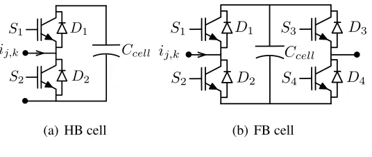
Since semiconductor losses represent the major portion of the total converter station losses, all the other losses such as transformer windings, passive components etc. have been excluded. The IGBT losses consist of conduction losses during the ON state, and switching losses during the transition between ON and OFF states and vice versa. Tables 1 and 2 show the switching transitions and conduction paths corresponding to FB and HB cells shown in Fig. 2.
S1
S2
D1
D2
Ccell ij,k
(a) HB cell
S1
S2
S3
S4
D1
D2
D3
D4
Ccell ij,k
[image:7.612.174.442.192.305.2](b) FB cell
Figure 2: Cell topologies.
IGBTs exhibit both conduction and switching power losses. Typically, a piecewise representation (see 0data0 in (18), (21)) of switching energy during turn-on and turn-off events is used to calculate IGBT
switching losses, while the IGBT voltage drop is used to estimate conduction losses. The losses are cal-culated based on an initial junction temperature that is similar to ambientTamb. The voltage drop during
IGBT conduction can be defined as a function of arm current and operating temperature, as shown in(18):
Vcedata =V ce
|iarm|
np , ϑS
data
Vfdata =V f
|iarm|
np , ϑD
data
(18)
Vlosscell =Vcedata+Vfdata (19)
Temperature calculation is carried out using a steady-state thermal model, considering the thermal resis-tances for each part of an IGBT, according to(20).
ϑS =PcondS·(RjS+RcS +Rhs) +Tamb
ϑD =PcondD ·(RjD +RcD +Rhs) +Tamb
(20)
Table 1: HB cell operation
Current Cell state Transition Conduction Positive 0 to Vc D1ON,S2OF F D1
Vc to 0 D1OF F,S2ON S2
Negative 0 to Vc D2OF F,S1ON S1
[image:7.612.221.374.451.534.2]Table 2: FB cell operation
Current Cell state Transition Conduction
Positive
0 to Vc D1ON,S2OF F D1,D4
Vc to 0 D1OF F,S2ON S2,D4
0 to -Vc D4OF F,S3ON S2,S3
-Vc to 0 S3OF F,D4ON S2,D4
Negative
0 to Vc D2OF F,S1ON S1,S4
Vc to 0 S1OF F,D2ON D2,S4
0 to -Vc D3ON,S4OF F D2,D3
-Vc to 0 D3OF F,S4ON D2,S4
whereRj,Rc,Rhs are the junction-to-case, case-to-heat-sink and heat-sink-to-ambient thermal resistances
respectively. IGBT and diode conduction losses are calculated according to(21):
PcondS = 1 T
Rt
t−T Vcedata·
|iarm|
np ·Kuti·ns·np dt
PcondD = 1 T
Rt
t−T Vfdata ·
|iarm|
np ·Kuti·ns·np dt
(21)
wherensandnpare the number of series and parallel-connected IGBTs and diodes respectively, andKutiis
the utilization constant described by(30). The number of series and parallel connected IGBTs is described by(22)and(23)respectively:
ns =ceil
Vchain
Vigbt·Ncell
(22)
np =ceil
ij,k
Iigbt
(23)
whereVchainis the total voltage across the stack per arm, andIigbtandVigbtare the continuous rated current
and blocking voltage of a single IGBT respectively. The energy which is dissipated during the switching process can be defined as a function of the instantaneous arm current and the switching energy of the IGBT, as shown in(24). Thereafter, the switching losses are calculated according to(25).
Esw =
|iarm|
np
·
ESon +ESof f +EDof f
data
(24)
PswS =
1 T
t
X
t−T
Esw·Kuti·KT ·ns·np (25)
where KT, (defined in (26)), is a thermal correction factor and is utilized to normalize the temperature
according to the IGBT thermal model.
KT =
ϑS, ϑD
ϑmaxdata
(26)
2.4. Implementation of Arm model
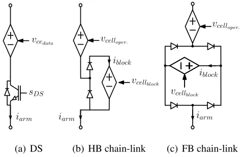
matrix; thus computation burden on the processor. The effectiveness of conventional electromagnetic tran-sient simulation program approach in simulation acceleration of full-scale converter models is widely ac-knowledged; however, much faster simulation speed could be achieved if the switching function modelling approach is adopted. [9]. Fig. 3 shows the switching function representation of the cells in terms of arm current and firing order, as it was described in(1)and(2). As the discrete integration of(2)determines the fidelity of the results, a small time step of5µsis necessary in order to achieve high accuracy.
iarm
scell−nj,k
C−cell1
iblock sblock
R
vlosscell
vcelloper.
[image:9.612.159.454.195.281.2]vcellblock
Figure 3: Cell voltage block diagram.
Moreover, an enhanced version of the switching model is used [22], by reflecting the switching losses through a calculated voltage dropvloss, as described later in(19). Fig. 4 illustrates the HB, FB cell stacks as
described in(3)and the DS. The controlled voltage source added into the DS model in Fig. 4(a) accounts for its switching and conduction losses, which are critical for accurate estimation of semiconductor losses in AAC. For example the chainlink in Fig. 4(a) in series with 4(c) resemble the arm of AAC, while the chainlink in Fig. 4(b) in series with 4(c) resemble the arm of MC-MMC.
vcedata
iarm sDS
(a) DS iarm
vcelloper.
vcellblock
iblock
(b) HB chain-link
vcellblock
vcelloper.
iarm
iblock
(c) FB chain-link
Figure 4: Equivalent representations of arm components.
[image:9.612.186.425.467.622.2]Table I, II R
Vcedata, Vfdata
(ESon, ESof f, EDon)data
P
s
cell|iarm|
np
i
armPcondcell
Pswcell ns, np
K
Tϑ
S, ϑ
DTable I, II
Figure 5: Block diagram of loss calculation scheme.
2.5. Controllers
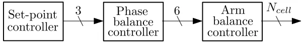
The generic control structure for all MMC and AAC being considered in this paper can be reduced, as shown in 6, which consist of set-point, phase balance and arm balance controllers. The details for each component of Fig. 6 will be elaborated further. For any converter topology, the principles for designing set- point and arm balance control can be similar. However, the actual implementation of phase balance control may differ from topology to topology depending on the different operational philosophies of each converter.
Set-point Phase
balance
Arm balance
6 Ncell
3
[image:10.612.155.456.366.409.2]controller controller controller
Figure 6: Generalised representation of converter control layers.
2.6. Set-point controller
Set-point controller determines the references for power, DC voltage, active and reactive current com-ponents as shown in Fig. 7. In such control scheme, there is a combination of decoupled current sub-controllers (i.e. outer and inner controller) alongside PI regulators and grid synchronization unit. The same set-point controller may be applied to any converter topology.
2.7. Phase balance controller
ωL dq abc PI PI dq abc P LL
Vdc∗
Vdc
P∗
P
Q
Q∗
i∗d
i∗q iq
id
v∗q
v∗q
vq
vd
vmd
vmq θ
θ
vj,ac
ij,ac i
d
iq
vd
vq
vj,ac
vm∗j
Outer controller Inner controller
Grid synchronization
PI PI
PI
[image:11.612.158.458.52.289.2]ωL
Figure 7: Set-point controller [5].
2.7.1. Circulating current controller (MMC)
There are various methods for active suppression of the circulating currents, which mainly affect the magnitude of the arm current, cell voltage ripple and the semiconductor losses. In this paper the DQ version of the Circulating Current Suppression Controller (CCSC) is used, as shown in Fig. 8 [6].
2ωLarm
dq
acb 2ωLarm
dq
abc vT HI
2θ
idif f,j
0
0
i2d
i2q
v∗mdif f,j
PI
PI
Pac
3 idif f,j
Vdc 2 PI PI PI i∗
dif f,j vm∗dc,j
Wsum,j
Wj∗
0 Wdif f,j
N ormalization
v∗mj
Circulating Current Suppression controller DQ
Energy controller
3rdHarmonic Injection
v∗
M M Cmj
v∗ mj,k Vdc 2θ Power to current
vd θ
[image:11.612.135.481.415.635.2]2.7.2. Energy controller (MMC)
The energy controller is employed to ensure energy balance between the upper and lower arms in each phase. It also decouples cell capacitor voltage regulation, and hence the AC voltage, from the DC link. In this manner, the energy stored in the cell capacitors can be manipulated to adjust DC components of the modulation signals, and the CSCC could potentially be eliminated [7].
2.7.3. Overlap angle controller (AAC)
This type of controller exists only in AAC converters, and regulates the period during which both arms conduct simultaneously. Although different implementations of overlap angle control, such as average energy and current-based control, exist [23, 24],such implementations may be inadequate if hardware delays are also considered. In the utilised models, therefore, fixed overlap angles (which are dependent upon modulation index) are adopted, as shown in Fig. 9.
N ormalization
v
∗mj
v
AAC∗mj
overlap
t
overv∗chainlink
mj,k
v∗DSmj,k
[image:12.612.165.452.311.375.2]φ
vT HIFigure 9: AAC phase controller.
2.7.4. Third Harmonic Injection (MMC/AAC)
Traditionally, the third harmonic injection (THI) technique is used to extend the modulation index linear range and improve DC link utilisation in order to improve converter PQ capability. The third harmonic voltage injected into the modulated signals of the MMC and AAC is described by(27):
vT HI =
min(v∗
ma, v
∗
mb, v
∗
mc) +max(v
∗
ma, v
∗
mb, v
∗
mc)
2 (27)
In AAC THI extends the period where the AAC operates as an MMC by modifying the voltage profile in the region of zero voltage crossover. This results in more in a efficient operation during the overlap period, and allows better energy equilibrium between the upper and lower arms regardless of the overlap period [25]. In AAC, THI removes the necessity for current injection from a star-connected transformer [26], and reduces the DC filtering requirements [25]. THI permits MMC to operate with higher range of converter AC voltage, which is beneficiary in terms of potential reduction in transformer and arm currents for the same power transfer [27]. Equations(28)and(29)describe the implementation of THI in AAC and MMC respectively.
vM M Cmj =vmj−vT HIj (29)
2.8. Arm balance controller
Arm balance controller is used both MMCs and AAC, to achieve equal voltage stress on the cell capac-itors and switching devices. In this paper a tolerance band CBA is utilised [8], which allows robust control operation, as it does not rely upon a complex sorting function and minimises computational effort as only the voltages that exceed the defined tolerance band need to be considered. The combination of tolerance band CBA with nearest level modulation allows well-balanced cell capacitors, as shown in Fig. 10(a) and 10(c). This is achieved by inserting or bypassing the cells which only operate for a short period during fun-damental cycle, as illustrated in Fig. 10(b) and 10(d). As a result, the overall average switching frequency of the converter remains low, as depicted in Fig. 10(e).
3. Design Methodology
This section describes the procedures followed for designing the main converter facets, such as the number of cells, and the passive component values, (i.e. cell capacitor and arm inductance). For ease of comparison, the design has been accomplished assuming the same rated power, DC voltage and voltage stress per device.
3.1. Number of cells and semiconductors
The number of cellsNcellis defined by two factors. Firstly, the AC power quality requirements need to
be fulfilled according to the grid code of each country. The higher the number of cells, the better the quality of AC voltage generated by the converter. The second factor is related to the converter’s operating power and DC voltage. Each cell must be rated to supportVcell =Vchain/Ncell. The use of parallel IGBTs reduces the
semiconductor losses and allows the use of lower current-rated IGBTs, while series connection reduces the number of cells, and hence power circuit and control complexity, and creepage and clearance requirements. Since series connection of IGBTs is not a straightforward task, it is more common to design cells to support voltage across single IGBT devices. Practically, the blocking voltageVigbtof an IGBT is selected to enable
stable operation and prolonged lifespan, and to sustain transient over-voltages. Consequently, 3.3 kV IGBTs [28] withVigbt =1.8 kV are used for the presented studies, and each cell switch consists of two
parallel-connected IGBTs. The converters being compared are assumed to have a similar utilisation factorKutiwith
1.85 1.86 1.87 1.88 1.89 1.28
1.44 1.6 1.76 1.92
T ime[s]
V
ol
tag
e
[kV]
V cellave V cell1 V cell244
(a) AAC capacitor voltages
1.85 1.86 1.87 1.88 1.89
−250 0 250 500 750 1000 1250 1500 1750 2000
T ime[s]
C
ur
rent
[A]
ia,u icell−244a,u
(b) AAC arm and cell currents
1.85 1.86 1.87 1.88 1.89 1.28
1.44 1.6 1.76 1.92
T ime[s]
V
ol
tag
e
[kV]
V cellave V cell1 V cell400
(c) MMC capacitor voltages
1.85 1.86 1.87 1.88 1.89
−2000 −1500 −1000 −500 0 500 1000
T ime[s]
C
ur
rent
[A]
ia,u icell−400a,u
(d) MMC arm and cell currents
1.85 1.86 1.87 1.88 1.89
160 170 180 190 200 210 220
T ime[s]
F
req
uency
[Hz] AAC F B−M M C HB−M M C M C−M M C
[image:14.612.152.459.55.476.2](e) Converter average switching frequency
Figure 10: The effect of tolerance band CBA.
factor Kuti describes the ratio between the required blocking voltage Vchain over the installed blocking
voltage capability of the chainlink, results in lower conduction losses as the silicon is used more effectively.
Kuti =
Vchain
Vigbt·ns·Ncell
(30)
To facilitate continuous operation during cell failure, redundant cells should be included in each stack, so that the failed cell can be replaced during a maintenance cycle. As a result the MMC and AAC topologies are tested with 400 and 244 [25] cells per arm respectively, which includes approximately 11% extra cells in each case. Since in HVDC applications an AAC must contribute to AC voltage or reactive power control,
itsVstack must be sized so that the modulation index can be controlled around the typical optimal operating
kVRM SLL, in order to achieve flexible operation as the AAC varies its power exchange.
3.2. Passive components sizing
Correct sizing of passive components (such as cell capacitors and arm inductance ) is critical for stable operation of AAC and MMC. Since cell capacitors in AAC and MMC experience low-frequency current, large cell capacitance will be required to ensure acceptable voltage ripple. To ensure stable operation over a wide modulation index, AAC energy storage capability is assumed to be similar to that of the MMC (i.e. 40 kJ/MW [29, 30].) The AAC arm inductance should be sufficient to enable the arm current to be transferred between arms during overlap, while providing a degree of current filtering [23]. In MMC the arm inductance (or accumulated DC side inductance [31]) can act as a filter for the circulating currents and to prolong current rise time in the event of a DC-side fault. An AAC requires a sizeable DC filter to attenuate 6th harmonic current and its multiples. However large filter capacitors may contribute to high
inrush currents during DC-side faults. In the studies presented in this paper, in order to ensure good quality of DC current and voltage over a wide operating range, the AAC DC filter components are chosen to be
LDCf = 10mH andCDCf = 28.15µF.
4. Results
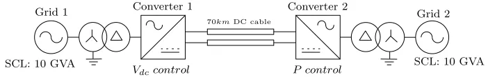
[image:15.612.186.429.558.713.2]In order to validate the operation of the converters and their dedicated controllers, a point-to-point HVDC network has been utilised as depicted in Fig. 11. The network consists of two converters in a symmetric monopole configuration which are connected via DC cables (Wideband cable model). In each case study, Converters 1 and 2 are of the same type in order to minimise any interactions due to hardware and controller design. Table 3 presents the rating and design specifications for each converter topology.
Table 3: Rating and design specifications
AAC MMC
S[MVA] 1045 1045
VDC [kV] 640 640
Transformer reactance [%] 18 18
Vchain/VDS[kV] 388/604
640/-Vgrid/Vconv[kV] 400/500 400/370
IGBT utilisation [%] 88.34 88.89 Arm inductance [mH] 11.14 65.36
Phase reactor [mH] 37.8
70kmDC cable Converter 1
P control Vdccontrol
Grid 1 Grid 2
SCL: 10 GVA Converter 2
[image:16.612.130.481.56.112.2]SCL: 10 GVA
Figure 11: Simulated DC network.
4.1. Power quality results
Fig. 12 shows that both converters have high-quality AC waveforms with very low total harmonic dis-tortion. However for future grids, which involve connections with multiple converters, DC power quality should also be considered. DC currentIDC determines the fluctuations in cable loading while DC voltage
affects the design of cable insulation [32]. According to IEC-60287 (the standard applicable to the condi-tions of steady-state operation of cables at all alternating voltages), the DC current response of the cables is a function of the differential temperature variation between the conductor and ambient. Cable insulation requirements are calculated based on temperature variation, which is affected by low-frequency current ripple [33].
1.85 1.86 1.87 1.88 1.89
−3000 −2000 −1000 0 1000 2000 3000
T ime[s]
AC
C
ur
rent
[A]
IT HDAAC= 1.093% IT HDM M C= 0.273%
(a) AC converter current
1.85 1.86 1.87 1.88 1.89
−4000 −3000 −2000 −1000 0 1000 2000 3000 4000
T ime[s]
AC
C
ur
rent
[A]
IT HDAAC= 1.091% IT HDM M C= 0.271%
(b) AC grid current
1.85 1.86 1.87 1.88 1.89 750 1000 1250 1500 1750 2000 2250
T ime[s]
D C C ur rent [A]
IDCrippleAAC= 20.8% IDCrippleM M C= 5.3%
(c) DC currents
1.85 1.86 1.87 1.88 1.89
−750 −500 −250 0 250 500 750
T ime[s]
AC V ol tag e [kV]
VT HDAAC= 20.942% VT HDM M C= 20.551%
(d) AC converter voltage
1.85 1.86 1.87 1.88 1.89
−600 −450 −300 −150 0 150 300 450 600
T ime[s]
AC V ol tag e [kV]
VT HDAAC= 0.599% VT HDM M C= 0.162%
(e) AC grid voltage
1.85 1.86 1.87 1.88 1.89 600
620 640 660 680
T ime[s]
D C V ol tag e [kV]
VDCrippleAAC= 1% VDCrippleM M C= 0.9%
[image:16.612.70.539.351.652.2](f) DC voltages
Figure 12: Converter voltage and current quality.
of the AAC exhibits high-magnitude of 6th harmonic ripple, which is due to the fundamental operating philosophy of AAC. Moreover, the quality of AAC and MMC DC waveforms is affected by the number of cells employed in each arm. A low number of cells per arm leads to higher voltage step transitions, and this causes larger voltage mismatches between the differential voltagevj,dif f and DC voltageVDC. By
comparing the DC current and DC voltage ripple for a 40-cell and a 400-cell MMC (see Fig. 13), it can be deduced that the higher the number of cells, the lower the DC current and voltage ripple range. The voltage and current ripples shown in DC sides are primarily of 300 Hz, which are more likely due to the interactions between different controller that maintain the internal dynamics of the MMC. Typically these ripples are attenuated by installing DC filter at converter DC bus.
1.85 1.86 1.87 1.88 1.89 0.9
0.95 1 1.05 1.1
T ime[s]
C
ur
rent
[p.u.]
IDCripple40
IDCripple400
(a) DC current measurement
0 1000 2000 3000 4000 5000 6000 0 5 10 15 20 300 Hz 600 Hz
F requency[Hz]
C
ur
rent
[A]
400-cell
(b) 400-cell current frequency spectrum
0 1000 2000 3000 4000 5000 6000 0 5 10 15 20 300 Hz 900 Hz 1200 Hz 1500 Hz 600 Hz
F requency[Hz]
C
ur
rent
[A]
40-cell
(c) 40-cell current frequency spectrum
1.85 1.86 1.87 1.88 1.89 0.98
0.99 1 1.01 1.02 1.03
T ime[s]
V
ol
tag
e
[p.u]
VDCripple40
VDCripple400
(d) DC voltage measurement
0 1000 2000 3000 4000 5000 6000 0
1 2 3
300 Hz
F requency[Hz]
V ol tag et [kV] 400-cell
(e) 400-cell voltage frequency spectrum
0 1000 2000 3000 4000 5000 6000 0
1 2
3 300 Hz
1500 Hz
2700 Hz 3900 Hz
F requency[Hz]
V ol tag et [kV] 40-cell
[image:17.612.57.552.261.562.2](f) 40-cell voltage frequency spectrum
Figure 13: DC voltage and current harmonics.
power, with reactive power varying between rated capacitor and rated inductive. Nevertheless, the quality of the DC waveforms in AAC worsen as its reactive power output increases, while the DC voltage ripple of the AAC quickly exceeds the 3% in the under-excitation region of the P-Q chart. In contrast, the plot in Fig. 14(d) shows that the AAC exhibits acceptable level of DC current ripples, independent of its reactive power output.
−00.3 −0.2 −0.1 0 0.1 0.2 0.3 1
2 3 4 5 6 7 8
AAC
MMC40 MMC400
Reactive power [pu]
VAC
LL
T
H
D
[%]
(a) AC converter voltage THD
−00.3 −0.2 −0.1 0 0.1 0.2 0.3 0.5
1 1.5 2 2.5
AAC
MMC40 MMC400
Reactive power [pu]
IAC
LL
T
H
D
[%]
(b) AC converter current THD
−00.3 −0.2 −0.1 0 0.1 0.2 0.3 1
2 3 4 5 6
AAC
MMC40
MMC400
Reactive power [pu]
V
dc
rippl
e
[%]
(c) DC voltage ripple
−00.3 −0.2 −0.1 0 0.1 0.2 0.3 10
20 30 40 50 60 70
AAC
MMC400
MMC40
Reactive power [pu]
I
dc
rippl
e
[%]
(d) DC current ripple
Figure 14: AC and DC power quality during variableQforP =1p.u.
The plots in Fig. 15 show the AAC DC current ripple when DC smoothing inductors with values of 10
mH, 50mH, 100mHand 300mHare considered. Moreover, Fig. 15 includes the DC current ripple when
an enhanced filter is used for 3rd, 6th and 12th harmonic attenuation, with lumped valuesL
DCf = 0.3 mH
andCDCf = 147.7 µF, which is similar to the short overlap method employed in [34]. The 12.5% (100
mH) DC inductance at the DC link of the AAC, reduces the DC current ripple to 10%, which is similar
[image:18.612.105.511.166.565.2]be observed in the DC current ripple when increased inductance of 300mH is used. DC inductance of 100mH and 300mH gives similar harmonic performance to the enhanced filter which included increased capacitance. It should be noted that, whilst the DC smoothing inductor reduces current ripple, it must be sized for rated DC current. Also, the increased capacitance of the enhanced filter will increase the amount of energy discharged during a DC fault.
−00.3 −0.2 −0.1 0 0.1 0.2 0.3 10
20 30 40 50 60 70 80
10mH
50mH
100mH
300mH
filter
Reactive power [pu]
AAC
I
dc
rippl
e
[image:19.612.207.402.175.341.2][%]
Figure 15: AACIDCripple for various installed DC inductance and filters
4.2. Power loss results
Pcond
S rec Pcond
Drec PswS r
ec PswD
rec
Pcond
S inv Pcond
Dinv PswS invPswD
inv 0 20 40 60 80 [%] IGBT 1 IGBT 2
(a) HB-MMC cell
Pcond
S rec Pcond
Drec PswS r
ec PswD
rec
Pcond
S inv Pcond
Dinv PswS invPswD
inv 0 10 20 30 40 50 60 [%] IGBT 1 IGBT 2 IGBT 3 IGBT 4
(b) FB-MMC cell
Pcond
S rec Pcond
Drec PswS r
ec PswD
rec
Pcond
S inv Pcond
Dinv PswS invPswD
inv 0 10 20 30 40 50 [%] IGBT 1 IGBT 2 IGBT 3 IGBT 4
[image:20.612.78.538.53.221.2](c) FB-AAC cell
Figure 16: Cell loss distribution over the total cell losses during inverter (inv) and rectification (rec) mode.
[image:20.612.188.426.332.507.2]Table 4 illustrates the contribution of FB and HB cells, and DS to conduction and switching losses in each topology, (where applicable).
Table 4: Loss contributions (inverter mode: P=1 p.u., Q=0 p.u.)
[kW] AAC FB HB MC
Cond. FB 4477 (44%)
11592
(91%)
-5794 (62%)
Cond. HB - - 4749
(81%)
2372 (26%) Cond. DS 4058
(39%) - -
-Sw. FB 1686
(17%)
1119
(9%)
-595 (6%)
Sw. HB - - 1136
(19%)
593 (6%)
Sw. DS 0
(0%) - -
−1 −0.6 −0.2 0.2 0.6 1 2.5
5 7.5 10 12.5
FBM M C
AAC
MCM M C
HBM M C
Inverter Rectif ier
Active power [p.u.]
T
otal
losses
[MW]
(a) 0 MVAr
−1 −0.6 −0.2 0.2 0.6 1
2.5 5 7.5 10 12.5
FBM M C
AAC
MCM M C
HBM M C
Inverter Rectif ier
Active power [p.u.]
T
otal
losses
[MW]
[image:21.612.72.549.58.290.2](b) 300 MVAr
Figure 17: Total semiconductor losses at various operation points for AAC and MMC.
Nonetheless, Table 5 shows that the reduction in the number of cells increases the switching losses, since a larger number of series-connected IGBTs switch for any given value of instantaneous current, while the conduction losses are only affected by the value ofKuti. Moreover, for a reduced number of levels,
PWM is employed, which may lead to even higher switching losses as the cells switch according to the carrier switching frequency [1]. This could be prevented by adopting distributed control with phase shifted carriers, as introduced in [36].
Table 5: Effect ofKution MMC
Ncell Kuti Cond. Losses[kW] Sw. Losses[kW]
20 0.99 4268 1246
100 0.89 4747 1222
400 0.89 4749 1136
5. Conclusions
• At unity power factor, the power quality at the DC side (DC current and voltage waveforms) of the AAC is marginally lower than that of the MMC, and that it deteriorates as power angle increases. This means that an HVDC link that employs an AAC requires substantial DC filtering to prevent penetration of the low-frequency harmonics from the converter into the DC side.
• The power quality at the AC side (AC current and voltage waveforms) of the AAC is marginally lower than that of the MMC. However, the rate of the deterioration of the AC power quality with power factor angle is much slower than that observed in the DC sides. This means smaller AC filters could be sufficient to meet the harmonic requirements at point of common coupling.
• The MMC with a reduced number of cells, exhibits lower DC-side power quality when compared to that with an increased number of cells. This implies that DC filters are necessary to prevent penetration of high-frequency harmonics from the converter into the DC link. There is only a slight difference in AC power quality between two configurations.
• The presented results revealed that in rectification mode, the AAC has higher losses than the MC-MMC, and the power losses of each converter converge as active power increases in inverter mode. Among modular designs, the FB-MMC and HB-MMC have been found to posses the highest and lowest losses respectively.
• The semiconductor power loss distributions between the individual switching devices of the FB cell in MMCs (FB-MMC, MC-MMC) and AACs, differ even when the operating conditions for both topologies are the same.
• The MMC with a reduced number of cells exhibits higher switching losses compared to an MMC with
a higher number of cells. This is on the grounds that the switching losses will be greatly influenced by the number of IGBTs to be switched simultaneously during turn-on and turn-off, for a given arm current.
• Studies also demonstrated that at rated power in rectification mode, the HB-MMC semiconductor
References
[1] G. L. B. Jacobson, P. Karlsson; and a. T. Jonsson, “VSC-HVDC transmission with cascaded two-level converters,” inCIGRE, August 2014.
[2] K. Friedrich, “Modern hvdc plus application of vsc in modular multilevel converter topology,” in2010 IEEE International Symposium on Industrial Electronics, July 2010, pp. 3807–3810.
[3] G. T. Son, H. J. Lee, T. S. Nam, Y. H. Chung, U. H. Lee, S. T. Baek, K. Hur, and J. W. Park, “Design and control of a modular multilevel hvdc converter with redundant power modules for noninterruptible energy transfer,”IEEE Transactions on Power Delivery, vol. 27, no. 3, pp. 1611–1619, July 2012.
[4] D. Jovcic, D. Van Hertem, K. Linden, J.-P. Taisne, and W. Grieshaber, “Feasibility of DC transmis-sion networks,” inInnovative Smart Grid Technologies, 2nd IEEE PES International Conference and Exhibition on, Dec 2011.
[5] G. P. Adam and B. W. Williams, “Half- and full-bridge modular multilevel converter models for sim-ulations of full-scale hvdc links and multiterminal dc grids,”IEEE Journal of Emerging and Selected Topics in Power Electronics, vol. 2, no. 4, pp. 1089–1108, Dec 2014.
[6] Q. Tu, Z. Xu, and L. Xu, “Reduced switching-frequency modulation and circulating current suppres-sion for modular multilevel converters,”IEEE Trans. on Power Delivery, vol. 26, no. 3, pp. 2009–2017, July 2011.
[7] S. Samimi, F. Gruson, P. Delarue, F. Colas, M. M. Belhaouane, and X. Guillaud, “MMC stored energy participation to the DC bus voltage control in an HVDC link,”IEEE Transactions on Power Delivery, vol. 31, no. 4, pp. 1710–1718, Aug 2016.
[8] F. Yu, W. Lin, X. Wang, and D. Xie, “Fast voltage-balancing control and fast numerical simulation model for the modular multilevel converter,”IEEE Transactions on Power Delivery, vol. 30, no. 1, pp. 220–228, Feb 2015.
[10] G. P. Adam, P. Li, I. A. Gowaid, and B. W. Williams, “Generalized switching function model of modular multilevel converter,” inIndustrial Technology (ICIT), 2015 IEEE International Conference on, March 2015, pp. 2702–2707.
[11] S. Rohner, S. Bernet, M. Hiller, and R. Sommer, “Modulation, losses, and semiconductor requirements of modular multilevel converters,” IEEE Transactions on Industrial Electronics, vol. 57, no. 8, pp. 2633–2642, Aug 2010.
[12] S. Rodrigues, A. Papadopoulos, E. Kontos, T. Todorcevic, and P. Bauer, “Steady-state loss model of half-bridge modular multilevel converters,” IEEE Transactions on Industry Applications, vol. 52, no. 3, pp. 2415–2425, May 2016.
[13] S. Norrga, X. Li, and L. Angquist, “Converter topologies for hvdc grids,” in2014 IEEE International Energy Conference (ENERGYCON), May 2014, pp. 1554–1561.
[14] A. Hassanpoor, A. Roostaei, S. Norrga, and M. Lindgren, “Optimization-based cell selection method for grid-connected modular multilevel converters,”IEEE Transactions on Power Electronics, vol. 31, no. 4, pp. 2780–2790, April 2016.
[15] H. Saad, K. Jacobs, W. Lin, and D. Jovcic, “Modelling of mmc including half-bridge and full-bridge submodules for emt study,” in2016 Power Systems Computation Conference (PSCC), June 2016, pp. 1–7.
[16] D. Trainer, W. Crookes, T. Green, and M. Merlin, “HVDC converter comprising fullbridge cells for handling a DC side short circuit,” May 23 2013, uS Patent App. 13/813,414. [Online]. Available: https://www.google.com/patents/US20130128636
[17] S. Norrga, “Modified voltage source converter structure,” Apr. 14 2011, wO Patent App. PCT/EP2009/062,966. [Online]. Available: https://www.google.com/patents/WO2011042050A1?cl= en
[18] G. P. Adam, K. H. Ahmed, and B. W. Williams, “Mixed cells modular multilevel converter,” in2014 IEEE 23rd International Symposium on Industrial Electronics (ISIE), June 2014, pp. 1390–1395.
[20] G. P. Adam and I. E. Davidson, “Robust and generic control of full-bridge modular multilevel con-verter high-voltage DC transmission systems,”IEEE Transactions on Power Delivery, vol. 30, no. 6, pp. 2468–2476, Dec 2015.
[21] H. Saad, X. Guillaud, J. Mahseredjian, S. Dennetire, and S. Nguefeu, “MMC capacitor voltage decou-pling and balancing controls,” in 2015 IEEE Power Energy Society General Meeting, July 2015, pp. 1–1.
[22] H. Saad, S. Dennetire, and J. Mahseredjian, “On modelling of MMC in emt-type program,” in2016 IEEE 17th Workshop on Control and Modeling for Power Electronics (COMPEL), June 2016, pp. 1–7.
[23] V. Najmi, R. Burgos, and D. Boroyevich, “Design and control of modular multilevel alternate arm converter (aac) with zero current switching of director switches,” in 2015 IEEE Energy Conversion Congress and Exposition (ECCE), Sept 2015, pp. 6790–6797.
[24] E. Farr, R. Feldman, A. Watson, J. Clare, and P. Wheeler, “A sub-module capacitor voltage balancing scheme for the alternate arm converter (aac),” in2013 15th European Conference on Power Electronics and Applications (EPE), Sept 2013, pp. 1–10.
[25] F. J. Moreno, M. M. C. Merlin, D. R. Trainer, T. C. Green, and K. J. Dyke, “Zero phase sequence voltage injection for the alternate arm converter,” in11th IET International Conference on AC and DC Power Transmission, Feb 2015, pp. 1–6.
[26] F. J. Moreno, M. M. C. Merlin, D. R. Trainer, K. J. Dyke, and T. C. Green, “Control of an alternate arm converter connected to a star transformer,” in 2014 16th European Conference on Power Electronics and Applications, Aug 2014, pp. 1–10.
[27] R. Li, J. E. Fletcher, and B. W. Williams, “Influence of third harmonic injection on modular multilevel converter -based high-voltage direct current transmission systems,” IET Generation, Transmission Distribution, vol. 10, no. 11, pp. 2764–2770, 2016.
[28] Dynex, “Dim1500esm33-tl000,” November 2016, Single Switch IGBT Module.
[30] M. M. C. Merlin and T. C. Green, “Cell capacitor sizing in multilevel converters: cases of the modular multilevel converter and alternate arm converter,”IET Power Electronics, vol. 8, no. 3, pp. 350–360, 2015.
[31] D. Tzelepis, A. Dysko, G. Fusiek, J. Nelson, P. Niewczas, D. Vozikis, P. Orr, N. Gordon, and C. Booth, “Single-ended differential protection in MTDC networks using optical sensors,” IEEE Transactions on Power Delivery, vol. PP, no. 99, pp. 1–1, 2016.
[32] L. Paulsson, B. Ekehov, S. Halen, T. Larsson, L. Palmqvist, A. A. Edris, D. Kidd, A. J. F. Keri, and B. Mehraban, “High-frequency impacts in a converter-based back-to-back tie; the eagle pass installation,”IEEE Transactions on Power Delivery, vol. 18, no. 4, pp. 1410–1415, Oct 2003.
[33] M. Marzinotto and G. Mazzanti, “The statistical enlargement law for HVDC cable lines part 1: the-ory and application to the enlargement in length,” IEEE Transactions on Dielectrics and Electrical Insulation, vol. 22, no. 1, pp. 192–201, Feb 2015.
[34] E. M. Farr, R. Feldman, J. C. Clare, A. J. Watson, and P. W. Wheeler, “The alternate arm converter (aac) - short-overlap mode operation - analysis and design parameter selection,” IEEE Transactions on Power Electronics, vol. PP, no. 99, pp. 1–1, 2017.
[35] M. M. C. Merlin, D. S. Sanchez, P. D. Judge, G. Chaffey, P. Clemow, T. C. Green, D. R. Trainer, and K. J. Dyke, “The extended overlap alternate arm converter: A voltage source converter with dc fault ride-through capability and a compact design,”IEEE Transactions on Power Electronics, vol. PP, no. 99, pp. 1–1, 2017.

![Figure 7: Set-point controller [5].](https://thumb-us.123doks.com/thumbv2/123dok_us/1423143.95010/11.612.135.481.415.635/figure-set-point-controller.webp)