Modular input-parallel-output-series DC/DC converter control
with fault detection and redundancy
Yiqing Lian*, D. Holliday
†, S. Finney
§*†§University of Strathclyde, 204 George Street, Glasgow, G1 1XW
Keywords: DC/DC converter, IPOS connection, Power sharing, Lyapunov controller, n+1 redundancy.
Abstract
Large offshore wind farms will require an extensive sub-sea power network to provide internal interconnection. Present solutions are based around conventional medium-voltage AC architectures. This paper proposes an alternative DC collection network based around modular DC/DC converters with input-parallel-output-series (IPOS) connection. Small-signal analysis of the converter is presented, to assist in control scheme development for the converter input and output stages. A Lyapunov controller is embedded within the conventional output voltage sharing control loop. A master-slave control scheme is proposed to ensure power sharing under a range of operating conditions, and provides fault-tolerant operation since the status of ‘master’ can be reallocated in the event that the present ‘master’ module fails.
1 Introduction
[image:1.595.351.506.406.541.2]In comparison with an AC network, a DC collection grid offers a number of potential benefits. The use of DC can better utilise the cable voltage rating and eliminates the charging current associated with long AC cables. These issues may become of increasing importance as the capacity and area of offshore wind farms increase. A medium-voltage DC collection grid also has the potential to reduce losses through the use of medium-voltage converters and better optimisation of conversion stages [1]. Additionally, a DC collection grid may reduce the size and weight of the required plant and power units [1]. Present offshore farms connect to conventional 50 or 60Hz AC systems by employing mains-frequency transformers to step up the generator output voltage to collection network voltage levels. Advances in DC/DC converters, particularly High-Frequency (HF) technologies [2, 3], allow the heavy line-frequency transformer in an AC grid to be replaced by a high- or medium-frequency transformer, leading to significant weight and size savings.
Fig.1 illustrates AC and DC options for the collection grid. In a DC collection grid, each individual wind turbine outputs DC from a fully rated DC/DC converter that replaces the conventional DC/AC stage of the back-to-back converter. Currently, there is uncertainty regarding the architectures and control approaches that enable this high-capacity DC/DC
power conversion. One possible solution is to use modular multilevel DC/DC converter (MMC) technology which has been widely studied for HVDC and MVDC [4, 5]. Modular multilevel approaches to high-voltage conversion have achieved significant gains in HVDC applications. The effectiveness of such techniques is, however, limited in DC/DC applications [4, 5]. Instead, a more compact and lighter design that uses a few modules arranged in a parallel-series topology could provide a replacement for a conventional single converter that uses high-voltage valves comprising several series-connected switching devices to enable operation at medium-voltage. In contrast to the topology where a single converter is managing all the power, in IPOS connected-converter the power is equally shared by all the modules.
Fig.1 Offshore wind farm AC and DC collection grids
1
o
V+ −
2
o
V+ −
3
o
V+ −
4
o
V+ −
o V
+
[image:1.595.350.502.573.719.2]−
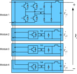
Fig.2 IPOS converter system topology4-module example. The proposed converter has an input parallel connection to provide current sharing, with each module being subjected to reduced current stress. This, in turn, simplifies converter design and manufacture. The series connection of the high-voltage side supports the collection network voltage. The modularity feature allows distribution of power management requirement among multiple modules. The modular architecture offers other advantages such as internal fault tolerance, as a result of (n+k) designed redundancy, and reduced filter size resulting from interleaved control [13-16].
Currently, the open literature contains few publications in the field of the IPOS converter and its control strategy. Normally, the average active sharing method or the master-slave active sharing method is chosen to solve the power sharing issue under any steady-state condition with mismatched components among the modules, and other challenging conditions such as inconformity of the transfer function, switching delay and discontinuity caused by the switching time delay, and input voltage disturbance [6]. In the master-slave control method, the master module is responsible for load regulation whilst the slaves ensure equal current and voltage sharing among the modules. Compared to the average active sharing method, fault-ride-through under module failure may be achieved more simply using master-slave control, with input current and output voltage being evenly shared among the remaining healthy modules. For existing control schemes, fault detection and protection methods for input-parallel-output-series connected DC/DC converters are not reported in the literature.
This study presents a control strategy based on a ‘master-slave’ scheme that enables power sharing between modules in an IPOS DC/DC converter under any steady-state condition where there is mismatch between module components, and which achieves ride-through of internal faults such as module failure. The proposed control scheme avoids the problems associated with ensuring (n+1) redundancy in the event of a fault in the master module that are characteristic of fixed ‘master-slave’ control schemes.
The paper is organised as follows: Controller design for an IPOS connected system with a full-bridge (FB) DC/DC converter is presented in Section 2. The response of the control system to abnormal fault conditions is also analysed, and a fault detection and protection scheme is proposed and presented. Section 3 presents the simulation results and the conclusions are presented in Section 4.
2 Control Theory
2.1 Small-Signal Modelling of an IPOS-Connected DC/DC Converter
The efficiency of each module is assumed to be 100% and there are n modules in total. The relationship between input and output power can be obtained for each module:
1 1
2 2
in in o o
in in o o
in inn on o
V I V I V I V I
V I V I
= =
⎧ ⎪ ⎪ ⎪⎪ ⎨ ⎪ ⎪ ⎪
⎪⎩ =
i i i
(1)
where Vin is the DC input voltage, Iin1, Iin2,…, Iinn are the module input currents, Vo1, Vo2,…, Von are the module output voltages, and Io is the load current. In the steady-state condition, the average filter capacitor current is zero. The filter inductor current ripple is therefore very small. If output voltage sharing (OVS) is achieved, then, Vo1=Vo2=…=Von. Substituting this result for OVS into (1), gives:
1 2
...
in in inn
I
=
I
= =
I
(2)It should be noted that input current sharing (ICS) is automatically achieved as long as OVS is achieved. Alternatively, if all modules share the same input current, then output voltage sharing is also achieved. In this study, OVS is applied to achieve power balancing.
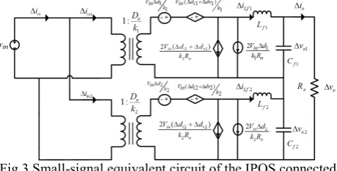
[image:2.595.309.548.529.650.2]The small-signal equivalent circuit of two IPOS connected PS-FB converters, shown in Fig.3, is given as an example, where k1 and k2 are the transformer turn ratios, Lr is the transformer leakage inductance, De is effective duty ratio per module [7], Lf1, Lf2, Cf1 and Cf2 are filter inductances and capacitances for modules 1 and 2 respectively, input voltage perturbation is represented by ∆vin, input current perturbations for the two modules are ∆iin1 and ∆iin2 respectively, filter inductor current and capacitor voltage perturbations are represented by ∆ilf1,∆ilf2,∆vo1, ∆vo2 respectively, ∆d1and ∆d2 are duty ratio perturbations, and ∆dv1, ∆dv2, ∆di1 and ∆di2 respectively represent duty ratio perturbations due to input voltage and output current, and are defined in (3) [7].
1 2 2 2 1 1 2 2 8 8 4 4
r e s
v in
in o
r e s
v in in o r s i lf in r s i lf in
L D f
d v
k V R L D f
d v
k V R L f d i kV L f d i kV ⎧
Δ = Δ
⎪ ⎪ ⎪
Δ = Δ
⎪ ⎪ ⎨
⎪Δ = − Δ
⎪ ⎪
⎪Δ = − Δ
⎪⎩
(3)
It is assumed that two modules have the same effective duty ratio, transformer turns ratios, and capacitor and inductor values, i.e. k1=k2=k, Lf1=Lf2=Lf, Cf1=Cf2=Cf, and Cd1=Cd2=Cd. From Fig.3, equations (4) can be obtained:
(
)
(
)
(
)
(
)
1 1 1
2 2 2
1 1 1 1
2 2 1 1 2 2 2 1 2 2 V L V L 2V 2V in
l f o
i
e in
v i f
e in
v i f
in
in v i
e o in n in l v f o l f l i e f o D
d d d s
k k
D
d d d s
k k
k
d d d
D v i v v i v i i i i kR k
d d d
D kR
Δ
Δ + Δ
Δ
Δ + Δ
Δ
⎧
+ Δ + Δ + Δ =
⎪ ⎪
⎪ + Δ + Δ + Δ =
⎪⎪ ⎨
⎪ = Δ + Δ + Δ +
⎪ ⎪
⎪ = Δ + Δ + Δ Δ
⎩ Δ +
⎪
Δ (4)
Module voltage perturbations can be obtained as (5):
(
)
(
)
1 2 1 1 2 2 1 2 1 1 o l f f o l f o o o o o f o sC R s v v v i v v C v R i⎡ Δ + Δ ⎤
Δ ⎢Δ ⎥
⎢ ⎥
⎣ ⎦
⎡ Δ + Δ ⎤
Δ ⎢Δ ⎥
⎢ ⎥ ⎣ ⎧ = − ⎪ ⎪ ⎨ − ⎦ ⎪ = ⎪ ⎩ (5)
which can be rewritten as (6):
1 2
2 2 2 2
1 2
2 2 2
2 2 1 1 1 2 2 1 1 2 2 f o
l f l f
f o f f o f
f o
l f l f
f o f
o
f o f
o
sC R
i i
s C R sC s C R sC
sC R
i i
s C R sC s C R
v
sC v
+
⎧
= Δ − Δ
⎪
+ +
⎪ ⎨
+
⎪ = − Δ + Δ
+ +
⎩
Δ
⎪Δ
(6)
Based on (6), the transfer function between module voltages and currents can be obtained in matrix form (7):
11 12 21 2 1 1 2 2 2 l f o
o l f
G G G i v i G v ⎡ ⎤ ⎡ ⎤ ⎡ ⎤ = ⎢ ⎥ ⎢ ⎥ ⎢ ⎥ ⎢ ⎥ ⎣ ⎦
⎣Δ ⎦ ⎣Δ ⎦
Δ Δ (7) where: 12 1 21
1 22 2 2
2 2 1 2 1 2 f o
f o f
f o f
sC R
G G
s C R sC
s C R sC
G =G
+ ⎧ = = ⎪ + ⎪ ⎨ ⎪ = − ⎪ + ⎩ (8)
Addition of the first two equations in (4) gives:
(
1 1 1 2 2)
1
2
1 2 2
2 V
L
e in
v in
l f o f l f o
i v i
f
v
i v sL
D
d d d d d d
k k
s i v
+ Δ + Δ + Δ + Δ + Δ + Δ
Δ
Δ + Δ + Δ +
=
Δ (9)
Assuming that ∆vin=0, and ∆dk=0 (k=1,2 and k≠j), and substituting (5) into (9), the relationship between load voltage and duty ratio is obtained as (10):
2
2 2
/
2 4 8
1
o in
ovd
f
j r s r s
f f f
o o
v V k
G
L
d L f L f
L C s C s
R k k R
Δ
= =
Δ ⎡ ⎤
+⎢ + ⎥ + +
⎣ ⎦
(10)
From (10), the control-to-output current ratio can be obtained as (11), by assuming ∆vin=0, and ∆dk=0 (k=1,2 and k≠j):
2 2 2 / 4 8 2 o oi j in
r s o r s
f f o f f
i G
d
V k
L f R L f
L C R s L C s
k k Δ = Δ = ⎡ ⎤ +⎢ + ⎥ + ⎣ ⎦ (11)
The load disturbance is measured by its effect on the load voltage, as shown in (12):
2
2
2 2
8 2
2 4 8
1 r s f o ov f
o r s r s
f f f
o o L f sL v k G L
i L f L f
L C s C s
R k k R
+ Δ
= =
Δ ⎡ ⎤
+⎢ + ⎥ + +
⎣ ⎦
(12)
Substituting (3) and (6) into (4), assuming ∆vin=0, yields (13):
1 2 2 2 1 2 2 2
2 2 2 1 2 2 2 2
1
V 4 1
L
2 2
1
V 1 4
L
2 2
f o
in r s
f lf lf
f o f f o f
f o
in r s
lf f lf
f o f f o f
C R s L f
d s i i
k C R s C s k C R s C s
C R s L f
d i s i
k C R s C s C R s C s k
⎧ ⎡ + ⎤
⎪ Δ =⎢ + + ⎥Δ − Δ
+ + ⎪ ⎢ ⎥ ⎪ ⎣ ⎦ ⎨ ⎡ + ⎤ ⎪
Δ = − Δ +⎢ + + ⎥Δ
⎪
+ ⎢ + ⎥
⎪ ⎣ ⎦
⎩
(13)
Rearranging (13), the relationship between duty ratio and inductor current can be represented as (14):
11 12 1
21 22
2 2
1 lf l f
i g g d
g g d
i Δ
⎡ ⎤ ⎡ ⎤ ⎡Δ ⎤
=
⎢Δ ⎥ ⎢ ⎥ ⎢Δ ⎥ ⎢ ⎥ ⎣ ⎦ ⎣ ⎦
⎣ ⎦ (14)
where: 11 22
2 2 2
2 2 2 2 2 2
12 21
2 2
2 2 2 2 2 2
1 4
V ( L )
2 2
4 4
( L ) ( L )
2 2
1
V ( )
2 2
4 4
( L ) ( L )
2 2
f o r s
in f
f o f
f o
o r s r s
f f
f o f f o f
in
f o f
f o
o r s r s
f f
f o f f o f
g g
sC R L f s
s C R sC k
sC R
R L f L f
k s s
s C R sC k s C R sC k
g g
s C R sC
sC R
R L f L f
k s s
s C R sC k s C R sC k
= ⎧ + + + + = + + + × + + + + ⎨ = − + = − + + + × + + + + ⎪ ⎪ ⎪ ⎪ ⎪ ⎪ ⎪ ⎪ ⎪ ⎪ ⎪ ⎪ ⎪ ⎪ ⎩ (15)
11 12
21 22
11 12 11 12 1
21 22 21 22 2
11 11 12 21 11 12 12 22 1
21 11 22 21 21 12 22 22 1
1
2 2
2
l f o
o l f
G G
G G
G G g g d
G G g g d
G g G g G g G g d
G g G g G g
v
g
v i
G d
i
⎡ ⎤
⎡ ⎤ ⎡ ⎤
= ⎢ ⎥
⎢ ⎥ ⎢ ⎥
⎢ ⎥
⎣ ⎦
⎣ ⎦ ⎣ ⎦
Δ
⎡ ⎤ ⎡ ⎤ ⎡ ⎤
=⎢ ⎥ ⎢ ⎥ ⎢Δ ⎥
⎣ ⎦ ⎣ ⎦ ⎣ ⎦
Δ
⎡
Δ Δ
Δ Δ
+ +
+
⎤ ⎡ ⎤
=⎢ ⎥ ⎢Δ ⎥
⎣ + ⎦ ⎣ ⎦
(16)
The transfer functions of the IPOS DC/DC converter derived in this section will be used in later to facilitate control design. 2.2 Lyapunov Closed-Loop Design for Output Voltage
From (10), the linear PI output voltage closed-loop controller is shown in Fig.4, and is based on a small-signal model which uses linearised large-signal state-space models around an equilibrium point to enable closed-loop design [8].
o
V∗
o V
⊗
Govdov G
/
i p p
s k k k
s
+ 1
m
[image:4.595.348.499.83.226.2]V
Fig.4 PI output voltage closed-loop controller
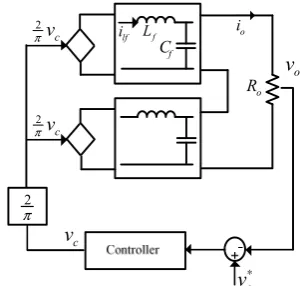
However, compared to a linear control technique such as PI control, some non-linear techniques can provide an improved transient response which is robust to load, input and parameter variations [9]. Most of the non-linear control laws are complex, which makes it difficult to apply, but the linearisation schemes have the advantage of reducing the converter model to an equivalent output filter model which significantly simplifies the robust control design process. A linearised control scheme for a single DC/DC converter, and a novel reduced equivalent model of the IPOS DC/DC converter incorporating closed-loop output voltage control are presented in Fig.5 [10] and Fig.6 respectively. These provide a linear representation of converter behaviour under large-signal variation which is suitable for faster control response and estimation of the converter state variables.
lf
i
v
oc
v
o
v
∗f
L
f C
o
i
o R
2
re c
v =πv
c
v
[image:4.595.65.292.83.181.2]δ δ
Fig.5 Closed-loop output voltage control configuration using the linearisation scheme
lf i
o
v
2
π c v 2
c
v
π
2
c
v
π
o
v∗ f
L
f
C o
i
o
R
Fig.6 Equivalent model for the IPOS DC/DC converter From Fig.6, and using (17) and (18), control variable vc is expressed in a second order transfer function of the output voltage (19).
1 2( 1 ) 2
l f
c o
f di
v v
dt =L π − (17)
2 2
( ) ( )
o o
l f o l f
f f o
dv v
i i i
dt =C − =C −R (18)
which leads to
2 2
( )
2
o c o
o
f f f o
v v v
v
C L πL R
= − + − (19)
To control the IPOS DC/DC converter output voltage, the output voltage error signal (20) is required [10]:
o o
e v v= −∗ (20)
In (21) it is assumed that v(x) is the first order control Lyapunov function and that α is proportionality constant:
2 1
( )
2
v= e+αe (21)
According to Lyapunov’s second condition, the derivative of
v is negative, where β is a strictly positive proportionality constant.
( )( ) 0
v= +e
α
e e+α
e = − <β
v (22)1
( ) ( )
2
e+
α
e = −β
e+α
e (23)Assuming vo* to be constant, e= −vo, e= −voand 2
2
( ) ( )
2 2 2
c o o
o o o o o
f f f o
v v v
v v v v v
C L L R
αβ β α
π
∗
= − − − = − − (24)
Substituting this result into (17) and (18) yields (25):
2
( )
8 4 2 4
f f f f
c o
o f
C L C L
v e e v
R C
αβ π π β α π
[image:4.595.54.277.576.659.2]It can be seen from (25) that the first and second terms represent a PD controller and will eventually decay to 0 as the system converges to the output voltage reference value. vo is a feed-forward term to speed start-up and to help stabilise the controller. Therefore, (25) can be rewritten as (26):
4
c p d o
v =k e k e+ +πv (26)
The transfer function between the output voltage and the adjusted output from the load voltage controller can be obtained from Fig.6:
2
4 1
1
oc
f f
G
L C s
π
=
+ (27)
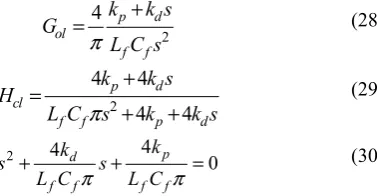
Thus, the closed-loop output voltage controller obtained using the Lyapunov approach is shown in Fig.7.
p d
k +k s o
v∗
2
4 1
1
f f
L C s
π +
oc
G
Ly
G
2
π
(a)
p d
k +k s
o
v∗
2
4 1
f f
L C s
π
oc G Ly
G
(b)
Fig.7Closed-loop Lyapunov controller (a) full structure (b) reduced equivalent controller due to feed-forward scheme Thus, the system open-loop, closed-loop and characteristic equation can be derived as (28-30):
2
4 p d
ol
f f
k k s G
L C s
π
+= (28)
2
4 4
4 4
p d
cl
f f p d
k k s H
L C s
π
k k s+ =
+ + (29)
2 4 d 4 p 0
f f f f
k k
s s
L C π L C π
+ + = (30)
[image:5.595.341.505.229.372.2]By designing the damping ratio and natural frequency from the system characteristic equation, the required closed-loop performance can be achieved. With the design specifications of 5% overshoot and 4ms settling time, the system root locus plot is given in Fig.8.
Fig.9 shows that the system bandwidth achieved using PI control is 1.29kHz, whilst that achieved using the Lyapunov controller is 2.39kHz and results in superior dynamic performance and disturbance rejection capability. Therefore, the control scheme requires one master module using Lyapunov control which produces the main control signal ∆i
(current command)to track the output voltage reference, and (n-1) slave modules which produce the voltage balancing
current reference quantities ∆ii (i=1,2,…,n-1). In this case,
vo1*= vo2*= vo(n-1)*= Vo /n. The sum of the current reference 1
1 n
i i
i
−
= Δ
∑
produced by all of the slave modules is subtracted from the current reference for the master module, and ∆i is added to the current reference of each slave module ∆ii (i=1,2,…,n -1). A third current control loop is added to guarantee current performance and the control scheme adjusts the system using individual inner current controllers, which are designed according to (14), for each module. The resulting control structure is shown in Fig.10.-6000 -5000 -4000 -3000 -2000 -1000 0 1000
-1500 -1000 -500 0 500 1000
1500 0.591
0.591 1.69e+03 Root Locus
Real Axis (seconds-1)
Im
ag
in
ar
y A
xi
s (
se
co
n
d
s
-1)
Fig.8Root locus for system with Lyapunov controller
Fig.9Closed-loop bandwidth 2.3 Fault Detection and Protection Issues
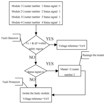
The multi-module DC/DC converter has internal fault management capability, in that faulty modules may be blocked in order to allow continued system operation without any performance degradation. Such a feature is normally achievable by incorporating redundant modules to allow re-configuration of the power circuit and bypassing of the faulty modules. The modularity feature allows (n+k) redundancy, where n is the number of modules required to ensure that each module operates within its voltage rating, and k is the number of redundant modules that can be used to replace k faulty modules and maintain an uninterrupted operation. (n+1) redundancy is introduced in this circuit.
[image:5.595.62.280.273.412.2] [image:5.595.320.528.402.549.2] [image:5.595.99.288.484.582.2]monitoring whether or not its output voltage and current fall outside predefined limits, e.g. voltage safety region [0.2Vo<Voi<0.3Vo] (i=1,2,…,4) for a 4-module converter. The faulty module is then isolated by blocking its front-end pulse width modulated H-bridge converter and bypassing its output diode bridge using a combination of a bypass switch and a bleed resistor to dissipate the energy stored in the filter capacitor. Any module can be operated in either an active state or a blocked state. If any slave unit fails, the system will locate the fault, block the faulty module and remain operational by simply changing the voltage reference to the slaves. For example, in a healthy n-module converter, the voltage reference for all slave modules is Vo/n, but if one module fails, the reference would become Vo/(n-1).
1
o
V ilf1
2
lf
i
lfn
i 1
on
V−ilfn−1
1
d
2
o
V
on
V
2
d
1
n
d−
n
d
o
V
⊗
ref
V
i
Δ
(a)
2
o
V ⊗
2 i
i
⊗
1
o
V ⊗
i
⊗
( 1)
o n
V − ⊗
( 1)n
i−
i
⊗
o
V
⊗ ⊗
ref
V
i
1
i
1
i
( 1)n
i−
vs
G
1
lf
I
oi
G
2
lf
I
⊗ Goi
1
lfn
I −
⊗ Goi
lfn
I
⊗ Goi
2 i
vs
G
vs
G
ov
G
1
o
V∗
2
o
V∗
( 1)
o n
V ∗ −
⊗
(b)
Fig.10(a) Output voltage Lyapunov control (b) Complete three loop control
The operation of the slaves is, however, dependent upon the master module control signals, i.e. if the master module malfunctions the overall system may fail [11]. In the previous case where a specific module is designated as ‘master’ under all conditions, the system will have a decreased reliability and modularity caused by a faulted master control module. In order to avoid system collapse, a ‘non-dedicated master’ approach is proposed, which enables the role of ‘master’ to be allocated to another healthy module in the event that the original master module fails. Because each module has the ability to becoming a master if required, any module may malfunction without further affecting the operation of the whole system.
Detailed description of the control is given as follows. For an
n-module converter, the system assigns each module with a specific numerical identifier (between 1 and n). The control system then assigns the status signal ‘0’ to module ‘1’, designating it as master, and status signal ‘1’ to the remaining
modules, thereby identifying them as the slaves. The fault detection and protection function is actived when a module’s output voltage or current falls outside predefined limits. If the module with status signal ‘1’, i.e. a slave module, fails the voltage reference for the slave modules is updated to Vo/(n-1). The role of ‘master’ is fixed to the designated module. When a failure of the master module occurs, module ‘2’ becomes the new master and the voltage reference for the slave modules is updated. Meanwhile, the system immediately isolates the faulted previous ‘master’ module. The failure flow graph for a 4-module converter is shown in Fig.11.
3 Simulation Results
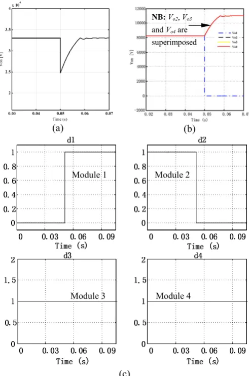
[image:6.595.55.290.244.527.2]In order to evaluate the proposed control scheme for the IPOS DC/DC converter, a system (shown in Fig.12) consisting of a generator, a fully-rated uncontrolled rectifier and an IPOS DC/DC converter with rated output power of 5MW, is simulated. Generator output voltage is 2500V at 50Hz, the high-frequency transformer operates at 5kHz and has a turns ratio of 2500:8250V, and the load voltage is maintained at 33kV. Module 1 is initially chosen as the master module. To test the effectiveness of the power balancing function, mismatches of +10% in transformer turns ratio of Module 1 and +10% in the output filter capacitor of Module 2 are introduced. Meanwhile, a permanent short-circuit fault is applied at the output terminals of Module 1 at t=50ms. Fig.13 presents selected simulation results.
Fig.11 Flow chart for the ‘non-dedicated master’ control scheme
Fig.13(a) shows the converter output voltage vo and Fig.13(b) shows the individual module output voltages (vo1, vo2, vo3 and
[image:6.595.347.526.418.598.2]the proposed control scheme manages failure of the master module, whilst ensuring continuous operation of and equal voltage sharing among the remaining healthy modules.
Fig.12High-power system used in fault study
Following the fault, the ‘non-dedicated master’ control function reallocates the role of ‘master’ to a healthy module, which in this case is Module 2. This process is illustrated in Fig.13(c) which shows the signals that define ‘master’ and ‘slave’ status of the modules. The ith module is defined as ‘master’ or ‘slave’ when di=0 or di=1 respectively. It can be seen that, following the fault, Module 1 is deselected as ‘master’ module and Module 2 is selected as the new ‘master’.
4 Conclusions
A ‘master-slave’ control strategy for IPOS DC/DC converters facilitates power sharing with mismatched components among the modules is proposed. The previous fixed ‘master-slave’ scheme can respond appropriately to slave module faults only, necessitating development of an enhanced controller based on the concept of the ‘non-dedicated master’ that permits arbitrary reallocation of the role of ‘master’ to another healthy module. The system has been verified through simulation of a fully-rated wind turbine module and the proposed control strategy can be extended to converters composed from any number of modules. The results show that the system exploits true (n+1) redundancy in the event that the master module is faulted.
Acknowledgements
The authors gratefully acknowledge the support of the EPSRC Centre for Doctoral Training in Wind Energy Systems (EP/G037728/1) and the ‘Underpinning Power Electronics 2012: Converters Theme’ research programme (EP/K035304/1).
(a) (b)
[image:7.595.305.551.81.452.2](c)
Fig.13 Response of (a) converter output voltage (b) module output voltage (c)allocation of ‘master’ and ‘slave’ roles
References
[1] D. M. Valcan, P. C. Kjar, L. Helle, S. Sahukari, M. Haj-Maharsi, and S. Singh, "Cost of energy assessment methodology for offshore AC and DC wind power plants," in Optimization of Electrical and Electronic Equipment (OPTIM), 2012 13th International Conference on, 2012, pp. 919-928. [2] P. Monjean, J. Delanoe, D. Marin, J. Auguste, C.
Saudemont, and B. Robyns, "Control strategies of DC-based offshore wind farm," in Power Electronics and Applications (EPE 2011), Proceedings of the 2011-14th European Conference on, 2011, pp. 1-9. [3] L. Yiqing and S. J. Finney, "DC collection networks
for offshore generation," in Renewable Power Generation Conference (RPG 2013), 2nd IET, 2013, pp. 1-4.
[4] I. A. Gowaid, G. P. Adam, A. M. Massoud, S. Ahmed, D. Holliday, and B. W. Williams, "Quasi Two-Level Operation of Modular Multilevel Converter for Use in a High-Power DC Transformer with DC Fault Isolation Capability," Power Electronics, IEEE Transactions on, vol. PP, pp. 1-1, 2014.
NB:Vo2, Vo3
and Vo4 are
superimposed
Module 1 Module 2
[image:7.595.60.275.131.244.2]
[5] D. Montesinos-Miracle, M. Massot-Campos, J. Bergas-Jane, S. Galceran-Arellano, and A. Rufer, "Design and Control of a Modular Multilevel DC/DC Converter for Regenerative Applications," Power Electronics, IEEE Transactions on, vol. 28, pp. 3970-3979, 2013.
[6] D. Qing, Q. Bojin, W. Tao, Z. Tao, and L. Xiao, "A High-Power Input-Parallel Output-Series Buck and Half-Bridge Converter and Control Methods," Power Electronics, IEEE Transactions on, vol. 27, pp. 2703-2715, 2012.
[7] R. Xinbo, C. Wu, C. Lulu, C. K. Tse, Y. Hong, and Z. Tao, "Control Strategy for Input-Series&Output-Parallel Converters," Industrial Electronics, IEEE Transactions on, vol. 56, pp. 1174-1185, 2009. [8] I. Batarseh and K. Siri, "Generalized approach to the
small signal modelling of DC-to-DC resonant converters," Aerospace and Electronic Systems, IEEE Transactions on, vol. 29, pp. 894-909, 1993.
[9] J. T. Matysik, "A New Method of Integration Control With Instantaneous Current Monitoring for Class D Series-Resonant Converter," Industrial Electronics, IEEE Transactions on, vol. 53, pp. 1564-1576, 2006.
[10] A. A. Aboushady, "Design, analysis and modelling of modular medium-voltage DC/DC converter based systems," Degree of Doctoer of Philosophy, Departement of Electronics and Electrical Engineering, University of Strathclyde, Glasgow, 2012.